ADS1231: I used ADS1231 chip to collect strain gauge data and found some problems during use. Please help me check the rationality of the circuit design

Part Number: ADS1231

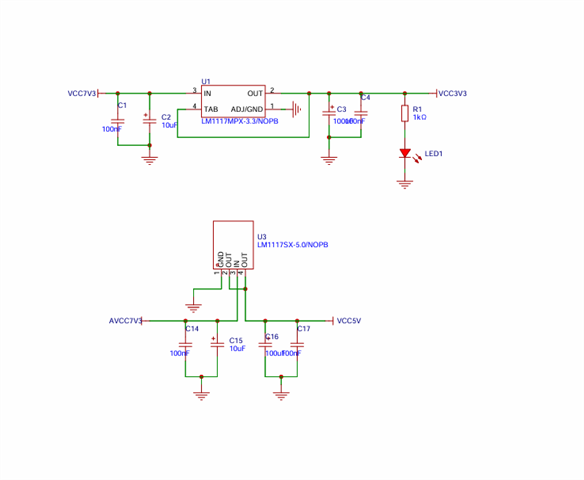
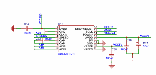
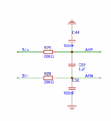
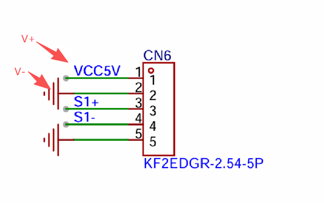
Hello engineer. I am using TI's ADS1231 chip to design a strain acquisition development board, and the schematic diagram is shown nearby. I found a problem while using it on site. I used 5V voltage to excite it, and theoretically the measurement range is within ± 20mv. Occasionally, the following situation occurs: after a full bridge strain gauge is connected, the collected voltage directly exceeds the range, reaching 20mv full range. I am not sure why this is happening? In my circuit design, there are several aspects that need to be considered: firstly, I did not make a single point connection between digital ground and analog ground for the ADS1231 chip. The definition of pins 2 and 11 of ADS1231 is "Groundford digital and analog supplies". Does this require distinguishing between digital ground and analog ground? Secondly, the VERFP pin of ADS1231 and the excitation voltage of the bridge are connected directly to a 5V LDO. The VERFN pin of ADS1231 and the excitation voltage of the bridge are connected directly to the GND of the circuit board, and the SW pin is also connected to GND. Is there any problem with this? Thirdly, my front-end acquisition circuit is designed with RC low-pass filtering, using 200 Ω and 1 μ F, and the calculated cut-off frequency is 8KHz. Is this filter reasonable? Please help me analyze the optimization or modification ideas for the problems I have encountered. Thank you!

LDOADS1231RCCONNECT

  • Hello!

    We have received your case and will take some time. Thank you for your patience.

  • Please ask the customer what bridge sensitivity is used, 3mV/V, 4mV/V, and so forth.  Or better, if the customer could provide the strain gauge part number.

    At first pass, I do not see any reason why the bridge measurement would exceed 20mV, unless the problem is with the strain gauge.

    As long as the the two GND pins on the ADS1231 are both connected to ground (preferably a ground plane on the PCB), the device should function correctly.  Also, for an input filter, 1uF is probably too large of a value.  1uF ceramic capacitors are multilayer construction, and can cause issues for an input filter.  It would be preferable to use 100nF C0G/NP0 capacitors for this filter, resulting in an input filter cutoff of 4kHz.  f-3dB=1/(2*PI*2*200ohm*100nF)=4kHz

  • The schematics look correct and do not indicate any reason why the readings would be at full scale range, unless the full bridge connected to the ADS1231 had a 20mV or greater output.

    When connecting the external full bridge and the readings are 20mV full scale, do the readings eventually fall back into the normal range?  Or do the readings remain at full scale 20mV?  Are you able to get correct readings by power-cycling the ADC circuit?

    Please provide any additional data, including an image of the board with the ADS1231, or any other observations that may help figure out the source of the problem.

    I assume communications over SCLK/DOUT are correct, but if the customer can capture a full data retrieval frame, similar to figure 19 in the datasheet, I will inspect to see if there is any kind of timing violation