Part Number: ADS1231
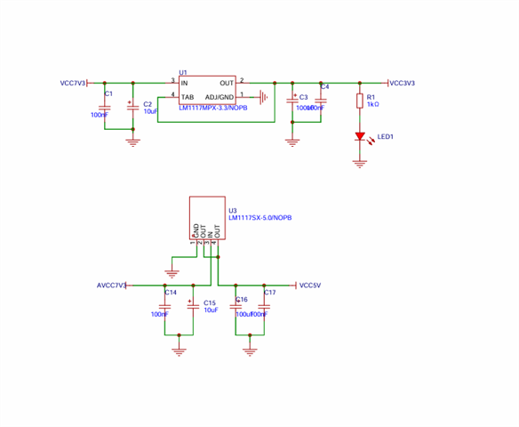
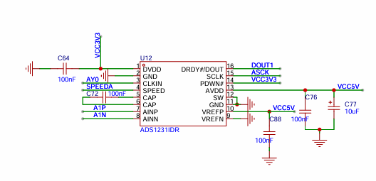
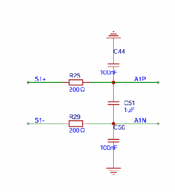
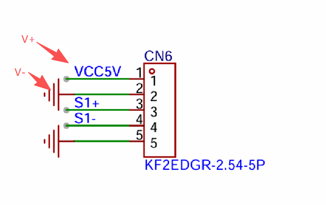
Hello engineer. I am using TI's ADS1231 chip to design a strain acquisition development board, and the schematic diagram is shown nearby. I found a problem while using it on site. I used 5V voltage to excite it, and theoretically the measurement range is within ± 20mv. Occasionally, the following situation occurs: after a full bridge strain gauge is connected, the collected voltage directly exceeds the range, reaching 20mv full range. I am not sure why this is happening? In my circuit design, there are several aspects that need to be considered: firstly, I did not make a single point connection between digital ground and analog ground for the ADS1231 chip. The definition of pins 2 and 11 of ADS1231 is "Groundford digital and analog supplies". Does this require distinguishing between digital ground and analog ground? Secondly, the VERFP pin of ADS1231 and the excitation voltage of the bridge are connected directly to a 5V LDO. The VERFN pin of ADS1231 and the excitation voltage of the bridge are connected directly to the GND of the circuit board, and the SW pin is also connected to GND. Is there any problem with this? Thirdly, my front-end acquisition circuit is designed with RC low-pass filtering, using 200 Ω and 1 μ F, and the calculated cut-off frequency is 8KHz. Is this filter reasonable? Please help me analyze the optimization or modification ideas for the problems I have encountered. Thank you!


