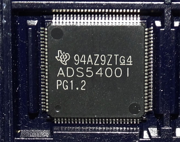
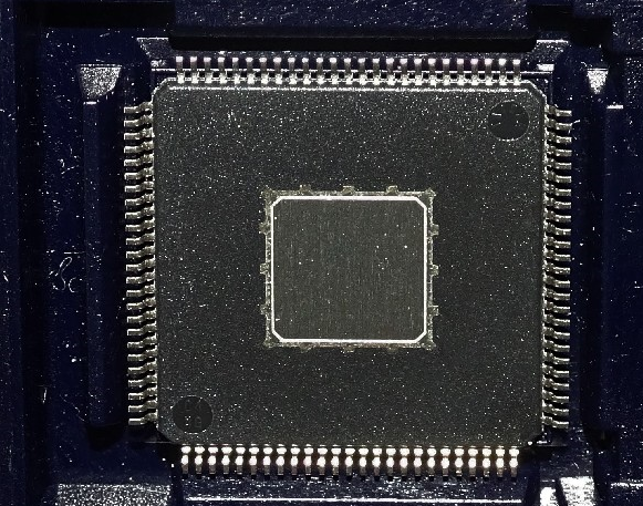
Part Number: ADS5400
hello!
1) the output voltage at the "VCM" pin does not correspond to the passport level of +2.5 V (at the supply voltage of the chip along the "AVDD5" line +5.0 V) and is +3.14B
2) the digital output data of the ADC is strongly distorted
3) - the identification data of the chips (Die revision), read via the SPI bus (0x01), do not correspond to the passport (0x61);
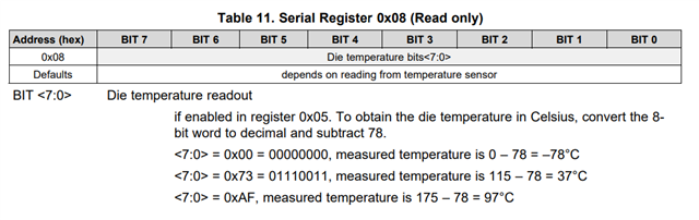
4) - the readings of the integrated temperature sensors of the chips, read over the SPI bus, do not correspond to reality (at +115 ° C), at a real temperature on the chip housing not exceeding +50 ° C\\
How can these problems be solved?