

Part Number: ADC3683EVM
The output of this board is a specific interface, and my FPGA does not have a corresponding interface, so I drew a PCB board to lead the corresponding signal to the PIN, but the output signal does not seem to be related to the input? I don't know where the problem is, here are some necessary pictures. I would like to know how to easily get my ADC output and process the data?
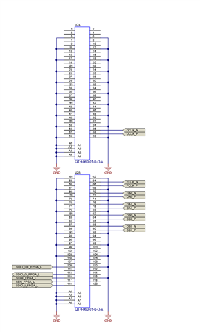 this is the connection diagram of the output signal
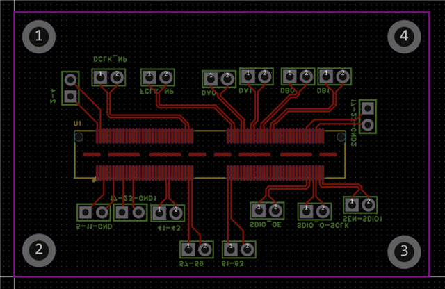
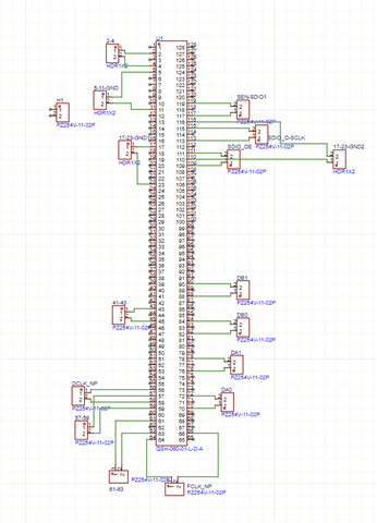 and I found that this QSH-060-01-L-D-A is the board mate of QTH-060-01-L-D-A in the schematic , and i drew a pcb to get these signals
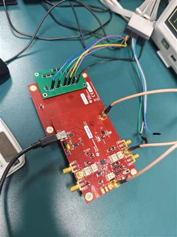 Here's my physical connection diagram. I've found that my output doesn't seem to be correct. And I don't know how to process the output data through the FPGA, because my FPGA is not the one that is included in the HSDC Pro.
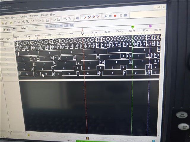 this is the waveform window of the logical analyzer , it shows the output code is wrong . and my threshold voltage is set to 1 V .
I suspected that my ADC was broken, but I did power down channels A and B through the operations in the GUI, and the output changed when I changed some settings.
