If you have a related question, please click the "Ask a related question" button in the top right corner. The newly created question will be automatically linked to this question.
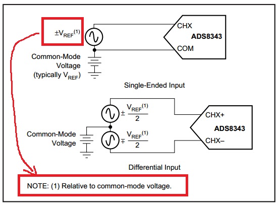
The ADS8343 is a 4-channel, 16-bit sampling Analog-to-Digital (A/D) converter with a synchronous serial interface. Typical power dissipation is 8mW at a 100kHz throughput rate and a +5V supply. The reference voltage (VREF) can be varied between 500mV and VCC/2, providing a corresponding input voltage range of ±VREF. The device includes a shutdown mode which reduces power dissipation to under 15µW. The ADS8343 is ensured down to 2.7V operation.
The ADS8341 is a 4-channel, 16-bit sampling Analog-to-Digital converter (A/D) with a synchronous serial interface. Typical power dissipation is 8mW at a 100kHz throughput rate and a +5V supply. The reference voltage (VREF ) can be varied between 500mV and VCC , providing a corresponding input voltage range of 0V to VREF . The device includes a shutdown mode that reduces power dissipation to under 15µW. The ADS8341 is tested down to 2.7V operation.
ABSOLUTE MAXIMUM RATINGS(1) +VCC to GND ........................................................................ –0.3V to +6V Analog Inputs to GND ............................................ –0.3V to +VCC + 0.3V Digital Inputs to GND ........................................................... –0.3V to +6V Power Dissipation .......................................................................... 250mW Maximum Junction Temperature ................................................... +150°C Operating Temperature Range ........................................–40°C to +85°C Storage Temperature Range .........................................–65°C to +150°C Lead Temperature (soldering, 10s) ............................................... +300°C NOTE: (1) Stresses above those listed under “Absolute Maximum Ratings” may cause permanent damage to the device. Exposure to absolute maximum conditions for extended periods may affect device reliability.
ABSOLUTE MAXIMUM RATINGS(1) +VCC to GND ........................................................................ –0.3V to +6V Analog Inputs to GND ............................................ –0.3V to +VCC + 0.3V Digital Inputs to GND ........................................................... –0.3V to +6V Power Dissipation .......................................................................... 250mW Maximum Junction Temperature ................................................... +150°C Operating Temperature Range ........................................–40°C to +85°C Storage Temperature Range .........................................–65°C to +150°C Lead Temperature (soldering, 10s) ............................................... +300°C NOTE: (1) Stresses above those listed under “Absolute Maximum Ratings” may cause permanent damage to the device. Exposure to absolute maximum conditions for extended periods may affect device reliability.
ABSOLUTE MAXIMUM RATINGS(1) +VCC to GND ........................................................................ –0.3V to +6V Analog Inputs to GND ............................................ –0.3V to +VCC + 0.3V Digital Inputs to GND ........................................................... –0.3V to +6V Power Dissipation .......................................................................... 250mW Maximum Junction Temperature ................................................... +150°C Operating Temperature Range ........................................–40°C to +85°C Storage Temperature Range .........................................–65°C to +150°C Lead Temperature (soldering, 10s) ............................................... +300°C NOTE: (1) Stresses above those listed under “Absolute Maximum Ratings” may cause permanent damage to the device. Exposure to absolute maximum conditions for extended periods may affect device reliability.