Part Number: LSF0108
The LSF0108 automatic bidirectional level conversion IC is used in the new project , and I would like to ask about its design. The circuit is shown in the figure.
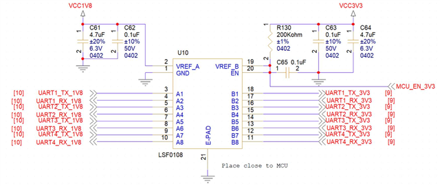
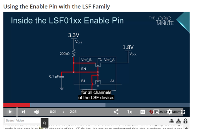
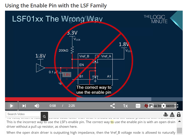
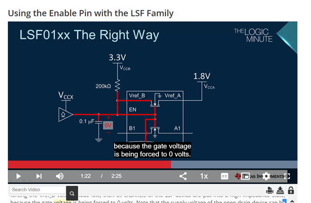
Question 1: Handling of EN pins
Now it is the combination of EN and VREF_B , which is pulled up to VCC3V3 through 200K , and then connected to the GPIO of the MCU ( MCU_EN_3V3 ). It is assumed that after the MCU initialization is completed, the pin is kept at a low level, open-drain output, and then released after the 1.8V and 3.3V levels are stable, and the level conversion function is turned on. Is this the right way to handle it? In addition, if it is not controlled by MCU , EN is directly pulled up to VCC3V3 through 200K , and it is automatically turned on after power-on. Will there be a problem?
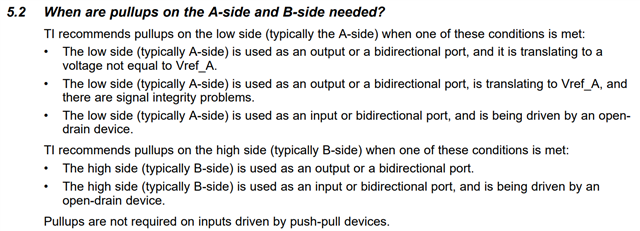
Question 2: Handling of pull-up resistors
I watched the video and said that the B side must have a pull-up resistor, and the A side depends on the situation (open-drain output is required). Does it mean that the UART_TX/RX on the B side in the above picture must be connected to the pull-up resistor? The resistance value should be selected according to the recommended value in the figure below?
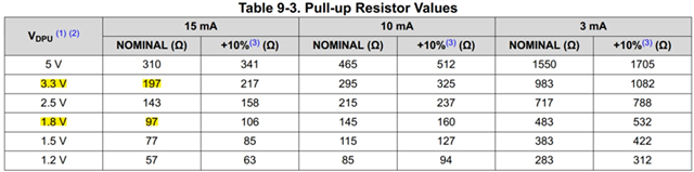
In addition, if it is a signal such as I2C/SDIO that requires an external pull-up, should pull-up resistors be connected on both sides of A/B ? The resistance value is also selected according to the above picture?