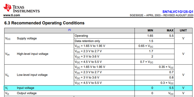
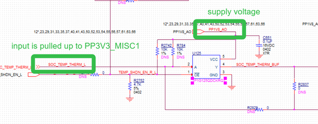
Part Number: SN74LVC1G125-Q1
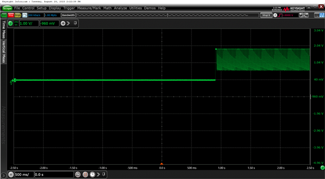
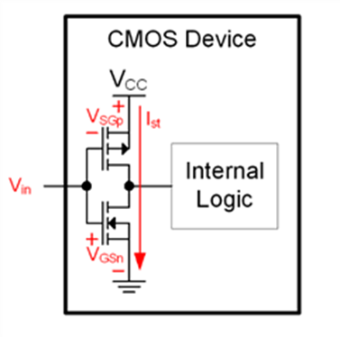
In our design, we have the input of 1P1G125QDCKRQ1 ramping up earlier than it's supply voltage, will this cause chip damage or abnormal performance?
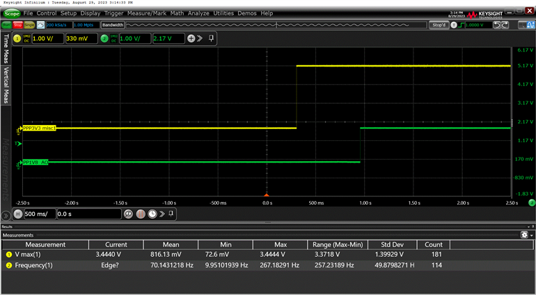
I also captured oscillating output of this chip while the input kept high, is this phenomena caused by chip damage?