This thread has been locked.
If you have a related question, please click the "Ask a related question" button in the top right corner. The newly created question will be automatically linked to this question.
你(们)好
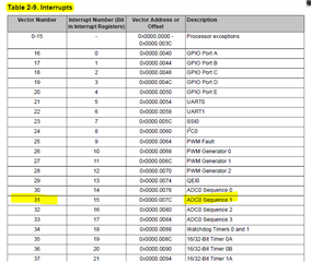
我使用 中断读取8个 ADC0通道, 但我还需要9个通道,我尝试使用不同的采样序列发生器、单独的 ISR 以及轮询所有 这些方法都不会为我提供第9个通道 ADC 数据。 这位于端口 E CH_8上,是否存在配置问题或缺少任何内容。
我的代码基于 Tiva 系列 SDK 版本:- TivaWare_C_Series-2.2.0.295
编译器是:- TI v 18.12.2.LTS
请帮助。
此致
霍迪达斯
#include <stdint.h> #include <stdbool.h> #include <stdio.h> //#include "inc/tm4c1294ncpdt.h" #include "driverlib/comp.h" #include "inc/hw_ints.h" #include "inc/hw_memmap.h" #include "inc/hw_adc.h" #include "inc/hw_types.h" #include "inc/hw_udma.h" #include "inc/hw_emac.h" #include "driverlib/debug.h" #include "driverlib/gpio.h" #include "driverlib/interrupt.h" #include "driverlib/pin_map.h" #include "driverlib/sysctl.h" #include "driverlib/uart.h" #include "driverlib/adc.h" #include "driverlib/udma.h" #include "driverlib/emac.h" #include "driverlib/flash.h" //#define TARGET_IS_BLIZZARD_RB1 #include "driverlib/rom.h" #include "driverlib/ssi.h" void gpioread(); //================================SPI SLAVE INITIALIZATION====================// #define NUM_SSI_DATA 5 uint32_t pui32DataTx[NUM_SSI_DATA]; uint32_t pui32DataRx[NUM_SSI_DATA]; uint32_t ui32Index; uint32_t adcBuffer2[9]; uint32_t ui32SysClock=0; bool in[25]; // // Interrupt Handler ADC0SS0 // void ADC0IntHandler(void) { // Clear interrupt Flag ADCIntClear(ADC0_BASE, 0); ADCSequenceDataGet(ADC0_BASE, 0, adcBuffer2); } void adc2_init(void) { uint32_t adcClock=0, adcDiv=0; // Enable the ADC0 peripheral SysCtlPeripheralEnable(SYSCTL_PERIPH_ADC0); SysCtlPeripheralEnable(SYSCTL_PERIPH_GPIOD); GPIOPinTypeADC(GPIO_PORTD_BASE, GPIO_PIN_7 | GPIO_PIN_6 | GPIO_PIN_5 | GPIO_PIN_4 | GPIO_PIN_3| GPIO_PIN_2| GPIO_PIN_1 | GPIO_PIN_0); SysCtlPeripheralEnable(SYSCTL_PERIPH_GPIOE); GPIOPinTypeADC(GPIO_PORTE_BASE, GPIO_PIN_5);// | GPIO_PIN_1 | GPIO_PIN_2 | GPIO_PIN_3); // Configure the ADC to use PLL at 480 MHz with Full rate devided by 30 to get 16 MHz ADCClockConfigSet(ADC0_BASE, ADC_CLOCK_SRC_PLL | ADC_CLOCK_RATE_FULL, 15); ADCSequenceDisable(ADC0_BASE, 0); ADCSequenceDisable(ADC0_BASE, 1); // Read the current ADC configuration adcClock=ADCClockConfigGet(ADC0_BASE, &adcDiv); // Hardware averageing: by a faktor of 2 -> 2,4,8,16,32,64 ADCHardwareOversampleConfigure(ADC0_BASE, 8); // ADC voltage-lvl reference set to intern ADCReferenceSet(ADC0_BASE, ADC_REF_INT); ADCReferenceSet(ADC0_BASE, ADC_REF_INT); // ADC Sequencer config: Source ADC0, Sequencer 0, Trigger: always, priority: 0 ADCSequenceConfigure(ADC0_BASE, 0, ADC_TRIGGER_ALWAYS, 0); ADCSequenceConfigure(ADC0_BASE, 1, ADC_TRIGGER_ALWAYS, 1); // ADC Sequencer step // 1. Source-ADC -> ADC0_BASE // 2. Source-Sequencer -> 0 // 3. Sample-Value depends in the depth of the FIFO, by Sequencer 0 it is up to 7 (0-7) // 4. Config-> select input-channel AINx, interrupt specification // ADCSequenceStepConfigure(ADC0_BASE, 1, 0, ADC_CTL_CH8 |ADC_CTL_IE|ADC_CTL_END); ADCSequenceStepConfigure(ADC0_BASE, 0, 0, ADC_CTL_CH4); ADCSequenceStepConfigure(ADC0_BASE, 0, 1, ADC_CTL_CH5); ADCSequenceStepConfigure(ADC0_BASE, 0, 2, ADC_CTL_CH6); ADCSequenceStepConfigure(ADC0_BASE, 0, 3, ADC_CTL_CH7); ADCSequenceStepConfigure(ADC0_BASE, 0, 4, ADC_CTL_CH12); ADCSequenceStepConfigure(ADC0_BASE, 0, 5, ADC_CTL_CH13); ADCSequenceStepConfigure(ADC0_BASE, 0, 6, ADC_CTL_CH14); ADCSequenceStepConfigure(ADC0_BASE, 0, 7, ADC_CTL_CH15 |ADC_CTL_IE|ADC_CTL_END ); IntPrioritySet(INT_ADC0SS0, 0x00); // ADC0SS0 Interrupt source ADCIntRegister(ADC0_BASE, 0, ADC0IntHandler); // Register Interrupt to NVIC IntRegister(INT_ADC0SS0, ADC0IntHandler); // ADC0 enable ADCIntEnable(ADC0_BASE, 0); // Interrupt ADC0SS0 enable IntEnable(INT_ADC0SS0); // Enable Global Interrupts IntMasterEnable(); ADCSequenceEnable(ADC0_BASE, 0); ADCSequenceEnable(ADC0_BASE, 1); } void SPI_Init() { // The SSI0 peripheral must be enabled for use. SysCtlPeripheralEnable(SYSCTL_PERIPH_SSI0); SysCtlPeripheralEnable(SYSCTL_PERIPH_GPIOA); GPIOPinConfigure(GPIO_PA2_SSI0CLK); GPIOPinConfigure(GPIO_PA3_SSI0FSS); GPIOPinConfigure(GPIO_PA4_SSI0XDAT0); GPIOPinConfigure(GPIO_PA5_SSI0XDAT1); GPIOPinTypeSSI(GPIO_PORTA_BASE, GPIO_PIN_5 | GPIO_PIN_4 | GPIO_PIN_3 | GPIO_PIN_2); // Configure and enable the SSI port for SPI master mode. Use SSI0, system clock supply, idle clock level low and active low clock in // freescale SPI mode, master mode, 1MHz SSI frequency, and 8-bit data. // For SPI mode, you can set the polarity of the SSI clock when the SSI unit is idle. You can also configure what clock edge you want to // capture data on. Please reference the datasheet for more information on the different SPI modes. SSIConfigSetExpClk(SSI0_BASE, ui32SysClock, SSI_FRF_MOTO_MODE_0, SSI_MODE_SLAVE, 1000000, 8); // Enable the SSI0 module. SSIEnable(SSI0_BASE); } void digital_init() { SysCtlPeripheralEnable(SYSCTL_PERIPH_GPION); // FOR LED GPIOPinTypeGPIOOutput(GPIO_PORTN_BASE, GPIO_PIN_1); GPIODirModeSet(GPIO_PORTN_BASE,GPIO_PIN_1,GPIO_DIR_MODE_OUT); GPIOPinWrite(GPIO_PORTN_BASE, GPIO_PIN_1, 0x02); GPIOPinWrite(GPIO_PORTN_BASE, GPIO_PIN_1, 0x02); //===========================Output Pins==============================// SysCtlPeripheralEnable(SYSCTL_PERIPH_GPIOA); GPIOPinTypeGPIOOutput(GPIO_PORTA_BASE, GPIO_PIN_0 |GPIO_PIN_1 ); GPIODirModeSet(GPIO_PORTA_BASE,GPIO_PIN_0 |GPIO_PIN_1 ,GPIO_DIR_MODE_OUT); SysCtlPeripheralEnable(SYSCTL_PERIPH_GPIOC); //GPIOUnlockPin(GPIO_PORTC_BASE, GPIO_PIN_4); GPIOPinTypeGPIOOutput(GPIO_PORTC_BASE, GPIO_PIN_4 |GPIO_PIN_5 |GPIO_PIN_6|GPIO_PIN_7 ); GPIODirModeSet(GPIO_PORTC_BASE,GPIO_PIN_4 |GPIO_PIN_5 |GPIO_PIN_6|GPIO_PIN_7,GPIO_DIR_MODE_OUT); SysCtlPeripheralEnable(SYSCTL_PERIPH_GPIOK); GPIOPinTypeGPIOOutput(GPIO_PORTK_BASE, GPIO_PIN_0 |GPIO_PIN_1 |GPIO_PIN_2 |GPIO_PIN_3 |GPIO_PIN_4 |GPIO_PIN_5 |GPIO_PIN_6|GPIO_PIN_7 ); GPIODirModeSet(GPIO_PORTK_BASE,GPIO_PIN_0 |GPIO_PIN_1 |GPIO_PIN_2 |GPIO_PIN_3 |GPIO_PIN_4 |GPIO_PIN_5 |GPIO_PIN_6|GPIO_PIN_7 ,GPIO_DIR_MODE_OUT); SysCtlPeripheralEnable(SYSCTL_PERIPH_GPIOP); GPIOPinTypeGPIOOutput(GPIO_PORTP_BASE, GPIO_PIN_0 |GPIO_PIN_1 |GPIO_PIN_2 |GPIO_PIN_3 |GPIO_PIN_4 |GPIO_PIN_5 ); GPIODirModeSet(GPIO_PORTP_BASE,GPIO_PIN_0 |GPIO_PIN_1 |GPIO_PIN_2 |GPIO_PIN_3 |GPIO_PIN_4 |GPIO_PIN_5 ,GPIO_DIR_MODE_OUT); SysCtlPeripheralEnable(SYSCTL_PERIPH_GPIOQ); GPIOPinTypeGPIOOutput(GPIO_PORTQ_BASE, GPIO_PIN_0 |GPIO_PIN_1 |GPIO_PIN_2 |GPIO_PIN_3 |GPIO_PIN_4 ); GPIODirModeSet(GPIO_PORTQ_BASE,GPIO_PIN_0 |GPIO_PIN_1 |GPIO_PIN_2 |GPIO_PIN_3 |GPIO_PIN_4 ,GPIO_DIR_MODE_OUT); //===========================Input Pins PORT L,M, F, G ,J==============================// SysCtlPeripheralEnable(SYSCTL_PERIPH_GPIOL); GPIOPinTypeGPIOInput(GPIO_PORTL_BASE, GPIO_PIN_0 |GPIO_PIN_1|GPIO_PIN_2|GPIO_PIN_3|GPIO_PIN_4|GPIO_PIN_5|GPIO_PIN_6|GPIO_PIN_7 ); GPIODirModeSet(GPIO_PORTL_BASE,GPIO_PIN_0 |GPIO_PIN_1|GPIO_PIN_2|GPIO_PIN_3|GPIO_PIN_4|GPIO_PIN_5|GPIO_PIN_6|GPIO_PIN_7,GPIO_DIR_MODE_IN); SysCtlPeripheralEnable(SYSCTL_PERIPH_GPIOM); GPIOPinTypeGPIOInput(GPIO_PORTM_BASE, GPIO_PIN_0 |GPIO_PIN_1|GPIO_PIN_2|GPIO_PIN_3|GPIO_PIN_4|GPIO_PIN_5|GPIO_PIN_6|GPIO_PIN_7 ); GPIODirModeSet(GPIO_PORTM_BASE,GPIO_PIN_0 |GPIO_PIN_1|GPIO_PIN_2|GPIO_PIN_3|GPIO_PIN_4|GPIO_PIN_5|GPIO_PIN_6|GPIO_PIN_7,GPIO_DIR_MODE_IN); SysCtlPeripheralEnable(SYSCTL_PERIPH_GPIOF); GPIOPinTypeGPIOInput(GPIO_PORTF_BASE, GPIO_PIN_0 |GPIO_PIN_1|GPIO_PIN_2|GPIO_PIN_3|GPIO_PIN_4); GPIODirModeSet(GPIO_PORTF_BASE,GPIO_PIN_0 |GPIO_PIN_1|GPIO_PIN_2|GPIO_PIN_3|GPIO_PIN_4,GPIO_DIR_MODE_IN); SysCtlPeripheralEnable(SYSCTL_PERIPH_GPIOG); GPIOPinTypeGPIOInput(GPIO_PORTG_BASE, GPIO_PIN_0 |GPIO_PIN_1); GPIODirModeSet(GPIO_PORTG_BASE,GPIO_PIN_0 |GPIO_PIN_1,GPIO_DIR_MODE_IN); SysCtlPeripheralEnable(SYSCTL_PERIPH_GPIOJ); GPIOPinTypeGPIOInput(GPIO_PORTJ_BASE, GPIO_PIN_0 |GPIO_PIN_1); GPIODirModeSet(GPIO_PORTJ_BASE,GPIO_PIN_0 |GPIO_PIN_1,GPIO_DIR_MODE_IN); } void main(void) { ui32SysClock=SysCtlClockFreqSet(SYSCTL_OSC_INT | SYSCTL_USE_PLL | SYSCTL_CFG_VCO_480, 120000000); // ADC Init adc2_init(); digital_init(); SPI_Init(); while(1) { GPIOPinWrite(GPIO_PORTN_BASE, GPIO_PIN_1, 0x02); GPIOPinWrite(GPIO_PORTA_BASE, GPIO_PIN_0, 0x01); GPIOPinWrite(GPIO_PORTA_BASE, GPIO_PIN_1, 0x02); GPIOPinWrite(GPIO_PORTC_BASE, GPIO_PIN_4, 0x10); GPIOPinWrite(GPIO_PORTC_BASE, GPIO_PIN_5, 0x20); GPIOPinWrite(GPIO_PORTC_BASE, GPIO_PIN_6, 0x40); GPIOPinWrite(GPIO_PORTC_BASE, GPIO_PIN_7, 0x80); GPIOPinWrite(GPIO_PORTK_BASE, GPIO_PIN_0, 0x01); GPIOPinWrite(GPIO_PORTK_BASE, GPIO_PIN_1, 0x02); GPIOPinWrite(GPIO_PORTK_BASE, GPIO_PIN_2, 0x04); GPIOPinWrite(GPIO_PORTK_BASE, GPIO_PIN_3, 0x08); GPIOPinWrite(GPIO_PORTK_BASE, GPIO_PIN_4, 0x10); GPIOPinWrite(GPIO_PORTK_BASE, GPIO_PIN_5, 0x20); GPIOPinWrite(GPIO_PORTK_BASE, GPIO_PIN_6, 0x40); GPIOPinWrite(GPIO_PORTK_BASE, GPIO_PIN_7, 0x80); GPIOPinWrite(GPIO_PORTP_BASE, GPIO_PIN_0, 0x01); GPIOPinWrite(GPIO_PORTP_BASE, GPIO_PIN_1, 0x02); GPIOPinWrite(GPIO_PORTP_BASE, GPIO_PIN_2, 0x04); GPIOPinWrite(GPIO_PORTP_BASE, GPIO_PIN_3, 0x08); GPIOPinWrite(GPIO_PORTP_BASE, GPIO_PIN_4, 0x10); GPIOPinWrite(GPIO_PORTP_BASE, GPIO_PIN_5, 0x20); GPIOPinWrite(GPIO_PORTQ_BASE, GPIO_PIN_0, 0x01); GPIOPinWrite(GPIO_PORTQ_BASE, GPIO_PIN_1, 0x02); GPIOPinWrite(GPIO_PORTQ_BASE, GPIO_PIN_2, 0x04); GPIOPinWrite(GPIO_PORTQ_BASE, GPIO_PIN_3, 0x08); GPIOPinWrite(GPIO_PORTQ_BASE, GPIO_PIN_4, 0x10); SysCtlDelay(ui32SysClock/12); GPIOPinWrite(GPIO_PORTN_BASE, GPIO_PIN_1, 0x00); GPIOPinWrite(GPIO_PORTA_BASE, GPIO_PIN_0, 0x00); GPIOPinWrite(GPIO_PORTA_BASE, GPIO_PIN_1, 0x00); GPIOPinWrite(GPIO_PORTC_BASE, GPIO_PIN_4, 0x00); GPIOPinWrite(GPIO_PORTC_BASE, GPIO_PIN_5, 0x00); GPIOPinWrite(GPIO_PORTC_BASE, GPIO_PIN_6, 0x00); GPIOPinWrite(GPIO_PORTC_BASE, GPIO_PIN_7, 0x00); GPIOPinWrite(GPIO_PORTK_BASE, GPIO_PIN_0, 0x00); GPIOPinWrite(GPIO_PORTK_BASE, GPIO_PIN_1, 0x00); GPIOPinWrite(GPIO_PORTK_BASE, GPIO_PIN_2, 0x00); GPIOPinWrite(GPIO_PORTK_BASE, GPIO_PIN_3, 0x00); GPIOPinWrite(GPIO_PORTK_BASE, GPIO_PIN_4, 0x00); GPIOPinWrite(GPIO_PORTK_BASE, GPIO_PIN_5, 0x00); GPIOPinWrite(GPIO_PORTK_BASE, GPIO_PIN_6, 0x00); GPIOPinWrite(GPIO_PORTK_BASE, GPIO_PIN_7, 0x00); GPIOPinWrite(GPIO_PORTP_BASE, GPIO_PIN_0, 0x00); GPIOPinWrite(GPIO_PORTP_BASE, GPIO_PIN_1, 0x00); GPIOPinWrite(GPIO_PORTP_BASE, GPIO_PIN_2, 0x00); GPIOPinWrite(GPIO_PORTP_BASE, GPIO_PIN_3, 0x00); GPIOPinWrite(GPIO_PORTP_BASE, GPIO_PIN_4, 0x00); GPIOPinWrite(GPIO_PORTP_BASE, GPIO_PIN_5, 0x00); GPIOPinWrite(GPIO_PORTQ_BASE, GPIO_PIN_0, 0x00); GPIOPinWrite(GPIO_PORTQ_BASE, GPIO_PIN_1, 0x00); GPIOPinWrite(GPIO_PORTQ_BASE, GPIO_PIN_2, 0x00); GPIOPinWrite(GPIO_PORTQ_BASE, GPIO_PIN_3, 0x00); GPIOPinWrite(GPIO_PORTQ_BASE, GPIO_PIN_4, 0x00); SysCtlDelay(ui32SysClock/12); //ADCSequenceDataGet(ADC0_BASE, 0, adcBuffer2); ADCSequenceDataGet(ADC0_BASE, 1, &adcBuffer2[9]); gpioread(); pui32DataTx[0] = 's'; pui32DataTx[1] = 'p'; pui32DataTx[2] = 'I'; pui32DataTx[3] = 'S'; pui32DataTx[4] = '\n'; for(ui32Index = 0; ui32Index < NUM_SSI_DATA; ui32Index++) { // Send the data using the "blocking" put function. This function // will wait until there is room in the send FIFO before returning. // This allows you to assure that all the data you send makes it into // the send FIFO. // SSIDataPutNonBlocking(SSI0_BASE, pui32DataTx[ui32Index]); //SSIDataGet(SSI0_BASE, &pui32DataRx[ui32Index]); SSIDataGetNonBlocking(SSI0_BASE, &pui32DataRx[ui32Index]); } } } void gpioread() { in[0]=GPIOPinRead(GPIO_PORTL_BASE, GPIO_PIN_0); in[1]=GPIOPinRead(GPIO_PORTL_BASE, GPIO_PIN_1); in[2]=GPIOPinRead(GPIO_PORTL_BASE, GPIO_PIN_2); in[3]=GPIOPinRead(GPIO_PORTL_BASE, GPIO_PIN_3); in[4]=GPIOPinRead(GPIO_PORTL_BASE, GPIO_PIN_4); in[5]=GPIOPinRead(GPIO_PORTL_BASE, GPIO_PIN_5); in[6]=GPIOPinRead(GPIO_PORTL_BASE, GPIO_PIN_6); in[7]=GPIOPinRead(GPIO_PORTL_BASE, GPIO_PIN_7); in[8]=GPIOPinRead(GPIO_PORTM_BASE, GPIO_PIN_0); in[9]=GPIOPinRead(GPIO_PORTM_BASE, GPIO_PIN_1); in[10]=GPIOPinRead(GPIO_PORTM_BASE, GPIO_PIN_2); in[11]=GPIOPinRead(GPIO_PORTM_BASE, GPIO_PIN_3); in[12]=GPIOPinRead(GPIO_PORTM_BASE, GPIO_PIN_4); in[13]=GPIOPinRead(GPIO_PORTM_BASE, GPIO_PIN_5); in[14]=GPIOPinRead(GPIO_PORTM_BASE, GPIO_PIN_6); in[15]=GPIOPinRead(GPIO_PORTM_BASE, GPIO_PIN_7); in[16]=GPIOPinRead(GPIO_PORTF_BASE, GPIO_PIN_0); in[17]=GPIOPinRead(GPIO_PORTF_BASE, GPIO_PIN_1); in[18]=GPIOPinRead(GPIO_PORTF_BASE, GPIO_PIN_2); in[19]=GPIOPinRead(GPIO_PORTF_BASE, GPIO_PIN_3); in[20]=GPIOPinRead(GPIO_PORTF_BASE, GPIO_PIN_4); in[21]=GPIOPinRead(GPIO_PORTG_BASE, GPIO_PIN_0); in[22]=GPIOPinRead(GPIO_PORTG_BASE, GPIO_PIN_1); in[23]=GPIOPinRead(GPIO_PORTJ_BASE, GPIO_PIN_0); in[24]=GPIOPinRead(GPIO_PORTJ_BASE, GPIO_PIN_1); }
你(们)好
[引用 userid="289369" URL"~/support/microcontrollers/other/f/other-microcontrollers-forum/993089/tm4c1294ncpdt-multiple-adc-channels-issue ]I 尝试使用不同的采样序列发生器、单独的 ISR 以及轮询所有 这些方法都不会为我提供第9个通道 ADC 数据。 这位于端口 E CH_8上、[/报价]请注意、每个序列发生器都有自己的中断矢量。 见下表。 我注意到您只注册 了 INT_ADC0SS0的 ADC0IntHandler。 您会想念 ADC0SS1。
您好!
这种方式是否与代码中的方式一样? 在这里、这也不起作用、我是寄存的独立 ISR 处理程序。
此致
霍迪达斯
void ADC0IntHandler(void) { // Clear interrupt Flag ADCIntClear(ADC0_BASE, 0); ADCSequenceDataGet(ADC0_BASE, 0, adcBuffer2); } void ADC1IntHandler(void) { // Clear interrupt Flag ADCIntClear(ADC0_BASE, 1); ADCSequenceDataGet(ADC0_BASE, 1, &adcBuffer2[9]); } void adc2_init(void) { uint32_t adcClock=0, adcDiv=0; // Enable the ADC0 peripheral SysCtlPeripheralEnable(SYSCTL_PERIPH_ADC0); SysCtlPeripheralEnable(SYSCTL_PERIPH_GPIOD); GPIOPinTypeADC(GPIO_PORTD_BASE, GPIO_PIN_7 | GPIO_PIN_6 | GPIO_PIN_5 | GPIO_PIN_4 | GPIO_PIN_3| GPIO_PIN_2| GPIO_PIN_1 | GPIO_PIN_0); SysCtlPeripheralEnable(SYSCTL_PERIPH_GPIOE); GPIOPinTypeADC(GPIO_PORTE_BASE, GPIO_PIN_5);// | GPIO_PIN_1 | GPIO_PIN_2 | GPIO_PIN_3); // Configure the ADC to use PLL at 480 MHz with Full rate devided by 30 to get 16 MHz ADCClockConfigSet(ADC0_BASE, ADC_CLOCK_SRC_PLL | ADC_CLOCK_RATE_FULL, 15); ADCSequenceDisable(ADC0_BASE, 0); ADCSequenceDisable(ADC0_BASE, 1); // Read the current ADC configuration adcClock=ADCClockConfigGet(ADC0_BASE, &adcDiv); // Hardware averageing: by a faktor of 2 -> 2,4,8,16,32,64 ADCHardwareOversampleConfigure(ADC0_BASE, 8); // ADC voltage-lvl reference set to intern ADCReferenceSet(ADC0_BASE, ADC_REF_INT); // ADC Sequencer config: Source ADC0, Sequencer 0, Trigger: always, priority: 0 ADCSequenceConfigure(ADC0_BASE, 0, ADC_TRIGGER_ALWAYS, 0); ADCSequenceConfigure(ADC0_BASE, 1, ADC_TRIGGER_ALWAYS, 1); // ADC Sequencer step // 1. Source-ADC -> ADC0_BASE // 2. Source-Sequencer -> 0 // 3. Sample-Value depends in the depth of the FIFO, by Sequencer 0 it is up to 7 (0-7) // 4. Config-> select input-channel AINx, interrupt specification // ADCSequenceStepConfigure(ADC0_BASE, 1, 0, ADC_CTL_CH8 |ADC_CTL_IE|ADC_CTL_END); ADCSequenceStepConfigure(ADC0_BASE, 0, 0, ADC_CTL_CH4); ADCSequenceStepConfigure(ADC0_BASE, 0, 1, ADC_CTL_CH5); ADCSequenceStepConfigure(ADC0_BASE, 0, 2, ADC_CTL_CH6); ADCSequenceStepConfigure(ADC0_BASE, 0, 3, ADC_CTL_CH7); ADCSequenceStepConfigure(ADC0_BASE, 0, 4, ADC_CTL_CH12); ADCSequenceStepConfigure(ADC0_BASE, 0, 5, ADC_CTL_CH13); ADCSequenceStepConfigure(ADC0_BASE, 0, 6, ADC_CTL_CH14); ADCSequenceStepConfigure(ADC0_BASE, 0, 7, ADC_CTL_CH15 |ADC_CTL_IE|ADC_CTL_END ); IntPrioritySet(INT_ADC0SS0, 0x00); IntPrioritySet(INT_ADC0SS1, 0x01); // ADC0SS0 Interrupt source ADCIntRegister(ADC0_BASE, 0, ADC0IntHandler); ADCIntRegister(ADC0_BASE, 1, ADC1IntHandler); // Register Interrupt to NVIC IntRegister(INT_ADC0SS0, ADC0IntHandler); IntRegister(INT_ADC0SS1, ADC1IntHandler); // ADC0 enable ADCIntEnable(ADC0_BASE, 0); ADCIntEnable(ADC0_BASE, 1); // Interrupt ADC0SS0 enable IntEnable(INT_ADC0SS0); IntEnable(INT_ADC0SS1); // Enable Global Interrupts IntMasterEnable(); ADCSequenceEnable(ADC0_BASE, 0); ADCSequenceEnable(ADC0_BASE, 1); }
您好!
我尝试修改现有的 TivaWare ADC 示例。 我在序列发生器1上使用 PE5 (AIN8)、但看不到任何问题。 您能否尝试以下示例并确认电路板上的 PE5 (AIN8)是否正常工作? 如果我连接到 VDD、则 AIN8上的值为4095。
#include <stdbool.h> #include <stdint.h> #include "inc/hw_memmap.h" #include "driverlib/adc.h" #include "driverlib/gpio.h" #include "driverlib/pin_map.h" #include "driverlib/sysctl.h" #include "driverlib/uart.h" #include "utils/uartstdio.h" //***************************************************************************** // //! \addtogroup adc_examples_list //! <h1>Single Ended ADC (single_ended)</h1> //! //! This example shows how to setup ADC0 as a single ended input and take a //! single sample on AIN8/PE3. //! //! This example uses the following peripherals and I/O signals. You must //! review these and change as needed for your own board: //! - ADC0 peripheral //! - GPIO Port E peripheral (for AIN8 pin) //! - AIN8 - PE5 //! //! The following UART signals are configured only for displaying console //! messages for this example. These are not required for operation of the //! ADC. //! - UART0 peripheral //! - GPIO Port A peripheral (for UART0 pins) //! - UART0RX - PA0 //! - UART0TX - PA1 //! //! This example uses the following interrupt handlers. To use this example //! in your own application you must add these interrupt handlers to your //! vector table. //! - None. // //***************************************************************************** //***************************************************************************** // // This function sets up UART0 to be used for a console to display information // as the example is running. // //***************************************************************************** void InitConsole(void) { // // Enable GPIO port A which is used for UART0 pins. // TODO: change this to whichever GPIO port you are using. // SysCtlPeripheralEnable(SYSCTL_PERIPH_GPIOA); // // Configure the pin muxing for UART0 functions on port A0 and A1. // This step is not necessary if your part does not support pin muxing. // TODO: change this to select the port/pin you are using. // GPIOPinConfigure(GPIO_PA0_U0RX); GPIOPinConfigure(GPIO_PA1_U0TX); // // Enable UART0 so that we can configure the clock. // SysCtlPeripheralEnable(SYSCTL_PERIPH_UART0); // // Use the internal 16MHz oscillator as the UART clock source. // UARTClockSourceSet(UART0_BASE, UART_CLOCK_PIOSC); // // Select the alternate (UART) function for these pins. // TODO: change this to select the port/pin you are using. // GPIOPinTypeUART(GPIO_PORTA_BASE, GPIO_PIN_0 | GPIO_PIN_1); // // Initialize the UART for console I/O. // UARTStdioConfig(0, 115200, 16000000); } //***************************************************************************** // // Configure ADC0 for a single-ended input and a single sample. Once the // sample is ready, an interrupt flag will be set. Using a polling method, // the data will be read then displayed on the console via UART0. // //***************************************************************************** int main(void) { #if defined(TARGET_IS_TM4C129_RA0) || \ defined(TARGET_IS_TM4C129_RA1) || \ defined(TARGET_IS_TM4C129_RA2) uint32_t ui32SysClock; #endif // // This array is used for storing the data read from the ADC FIFO. It // must be as large as the FIFO for the sequencer in use. This example // uses sequence 3 which has a FIFO depth of 1. If another sequence // was used with a deeper FIFO, then the array size must be changed. // uint32_t pui32ADC0Value[1]; // // Set the clocking to run at 20 MHz (200 MHz / 10) using the PLL. When // using the ADC, you must either use the PLL or supply a 16 MHz clock // source. // TODO: The SYSCTL_XTAL_ value must be changed to match the value of the // crystal on your board. // #if defined(TARGET_IS_TM4C129_RA0) || \ defined(TARGET_IS_TM4C129_RA1) || \ defined(TARGET_IS_TM4C129_RA2) ui32SysClock = SysCtlClockFreqSet((SYSCTL_XTAL_25MHZ | SYSCTL_OSC_MAIN | SYSCTL_USE_PLL | SYSCTL_CFG_VCO_480), 20000000); #else SysCtlClockSet(SYSCTL_SYSDIV_10 | SYSCTL_USE_PLL | SYSCTL_OSC_MAIN | SYSCTL_XTAL_16MHZ); #endif // // Set up the serial console to use for displaying messages. This is // just for this example program and is not needed for ADC operation. // InitConsole(); // // Display the setup on the console. // UARTprintf("ADC ->\n"); UARTprintf(" Type: Single Ended\n"); UARTprintf(" Samples: One\n"); UARTprintf(" Update Rate: 250ms\n"); UARTprintf(" Input Pin: AIN8/PE5\n\n"); // // The ADC0 peripheral must be enabled for use. // SysCtlPeripheralEnable(SYSCTL_PERIPH_ADC0); // // For this example ADC0 is used with AIN8 on port E7. // The actual port and pins used may be different on your part, consult // the data sheet for more information. GPIO port E needs to be enabled // so these pins can be used. // TODO: change this to whichever GPIO port you are using. // SysCtlPeripheralEnable(SYSCTL_PERIPH_GPIOE); // // Select the analog ADC function for these pins. // Consult the data sheet to see which functions are allocated per pin. // TODO: change this to select the port/pin you are using. // GPIOPinTypeADC(GPIO_PORTE_BASE, GPIO_PIN_5); // // Enable sample sequence 3 with a processor signal trigger. Sequence 3 // will do a single sample when the processor sends a signal to start the // conversion. Each ADC module has 4 programmable sequences, sequence 0 // to sequence 3. This example is arbitrarily using sequence 3. // ADCSequenceConfigure(ADC0_BASE, 3, ADC_TRIGGER_PROCESSOR, 0); // // Configure step 0 on sequence 1. Sample channel 8 (ADC_CTL_CH8) in // single-ended mode (default) and configure the interrupt flag // (ADC_CTL_IE) to be set when the sample is done. Tell the ADC logic // that this is the last conversion on sequence 1 (ADC_CTL_END). Sequence // 3 has only one programmable step. Sequence 1 and 2 have 4 steps, and // sequence 0 has 8 programmable steps. Since we are only doing a single // conversion using sequence 1 we will only configure step 0. For more // information on the ADC sequences and steps, reference the datasheet. // ADCSequenceStepConfigure(ADC0_BASE, 1, 0, ADC_CTL_CH8 | ADC_CTL_IE | ADC_CTL_END); // // Since sample sequence 1 is now configured, it must be enabled. // ADCSequenceEnable(ADC0_BASE, 1); // // Clear the interrupt status flag. This is done to make sure the // interrupt flag is cleared before we sample. // ADCIntClear(ADC0_BASE, 1); // // Sample AIN8 forever. Display the value on the console. // while(1) { // // Trigger the ADC conversion. // ADCProcessorTrigger(ADC0_BASE, 1); // // Wait for conversion to be completed. // while(!ADCIntStatus(ADC0_BASE, 1, false)) { } // // Clear the ADC interrupt flag. // ADCIntClear(ADC0_BASE, 1); // // Read ADC Value. // ADCSequenceDataGet(ADC0_BASE, 1, pui32ADC0Value); // // Display the AIN8 (PE5) digital value on the console. // UARTprintf("AIN8 = %4d\r", pui32ADC0Value[0]); // // This function provides a means of generating a constant length // delay. The function delay (in cycles) = 3 * parameter. Delay // 250ms arbitrarily. // #if defined(TARGET_IS_TM4C129_RA0) || \ defined(TARGET_IS_TM4C129_RA1) || \ defined(TARGET_IS_TM4C129_RA2) SysCtlDelay(ui32SysClock / 12); #else SysCtlDelay(SysCtlClockGet() / 12); #endif } }
您好!
不管怎样、我的问题 是9 个 ADC 通道。 当采用第9 个 ADC 通道时(任何通道为 第9个通道) 不起作用、并且所有其他 8个通道都起作用。 那么 、我应该 对 超过8 个 ADC 通道执行什么操作
此致
霍迪达斯
您好!
我修改了最后一个程序的位、以便在序列0中对 AIN0进行8次采样、而第9个通道 AIN8位于序列发生器1中。 我将 AIN8连接到3.3V、将 AIN0连接到 GND。 我能够看到正确测量了 AIN8。
#include <stdbool.h> #include <stdint.h> #include "inc/hw_memmap.h" #include "driverlib/adc.h" #include "driverlib/gpio.h" #include "driverlib/pin_map.h" #include "driverlib/sysctl.h" #include "driverlib/uart.h" #include "utils/uartstdio.h" //***************************************************************************** // //! \addtogroup adc_examples_list //! <h1>Single Ended ADC (single_ended)</h1> //! //! This example shows how to setup ADC0 as a single ended input and take a //! single sample on AIN8/PE3. //! //! This example uses the following peripherals and I/O signals. You must //! review these and change as needed for your own board: //! - ADC0 peripheral //! - GPIO Port E peripheral (for AIN8 pin) //! - AIN8 - PE5 //! //! The following UART signals are configured only for displaying console //! messages for this example. These are not required for operation of the //! ADC. //! - UART0 peripheral //! - GPIO Port A peripheral (for UART0 pins) //! - UART0RX - PA0 //! - UART0TX - PA1 //! //! This example uses the following interrupt handlers. To use this example //! in your own application you must add these interrupt handlers to your //! vector table. //! - None. // //***************************************************************************** //***************************************************************************** // // This function sets up UART0 to be used for a console to display information // as the example is running. // //***************************************************************************** void InitConsole(void) { // // Enable GPIO port A which is used for UART0 pins. // TODO: change this to whichever GPIO port you are using. // SysCtlPeripheralEnable(SYSCTL_PERIPH_GPIOA); // // Configure the pin muxing for UART0 functions on port A0 and A1. // This step is not necessary if your part does not support pin muxing. // TODO: change this to select the port/pin you are using. // GPIOPinConfigure(GPIO_PA0_U0RX); GPIOPinConfigure(GPIO_PA1_U0TX); // // Enable UART0 so that we can configure the clock. // SysCtlPeripheralEnable(SYSCTL_PERIPH_UART0); // // Use the internal 16MHz oscillator as the UART clock source. // UARTClockSourceSet(UART0_BASE, UART_CLOCK_PIOSC); // // Select the alternate (UART) function for these pins. // TODO: change this to select the port/pin you are using. // GPIOPinTypeUART(GPIO_PORTA_BASE, GPIO_PIN_0 | GPIO_PIN_1); // // Initialize the UART for console I/O. // UARTStdioConfig(0, 115200, 16000000); } //***************************************************************************** // // Configure ADC0 for a single-ended input and a single sample. Once the // sample is ready, an interrupt flag will be set. Using a polling method, // the data will be read then displayed on the console via UART0. // //***************************************************************************** int main(void) { #if defined(TARGET_IS_TM4C129_RA0) || \ defined(TARGET_IS_TM4C129_RA1) || \ defined(TARGET_IS_TM4C129_RA2) uint32_t ui32SysClock; #endif // // This array is used for storing the data read from the ADC FIFO. It // must be as large as the FIFO for the sequencer in use. This example // uses sequence 3 which has a FIFO depth of 1. If another sequence // was used with a deeper FIFO, then the array size must be changed. // uint32_t pui32ADC0Value[1]; uint32_t pui32ADC0Value2[8]; // // Set the clocking to run at 20 MHz (200 MHz / 10) using the PLL. When // using the ADC, you must either use the PLL or supply a 16 MHz clock // source. // TODO: The SYSCTL_XTAL_ value must be changed to match the value of the // crystal on your board. // #if defined(TARGET_IS_TM4C129_RA0) || \ defined(TARGET_IS_TM4C129_RA1) || \ defined(TARGET_IS_TM4C129_RA2) ui32SysClock = SysCtlClockFreqSet((SYSCTL_XTAL_25MHZ | SYSCTL_OSC_MAIN | SYSCTL_USE_PLL | SYSCTL_CFG_VCO_480), 20000000); #else SysCtlClockSet(SYSCTL_SYSDIV_10 | SYSCTL_USE_PLL | SYSCTL_OSC_MAIN | SYSCTL_XTAL_16MHZ); #endif // // Set up the serial console to use for displaying messages. This is // just for this example program and is not needed for ADC operation. // InitConsole(); // // Display the setup on the console. // UARTprintf("ADC ->\n"); UARTprintf(" Type: Single Ended\n"); UARTprintf(" Samples: One\n"); UARTprintf(" Update Rate: 250ms\n"); UARTprintf(" Input Pin: AIN8/PE5\n\n"); // // The ADC0 peripheral must be enabled for use. // SysCtlPeripheralEnable(SYSCTL_PERIPH_ADC0); // // For this example ADC0 is used with AIN8 on port E7. // The actual port and pins used may be different on your part, consult // the data sheet for more information. GPIO port E needs to be enabled // so these pins can be used. // TODO: change this to whichever GPIO port you are using. // SysCtlPeripheralEnable(SYSCTL_PERIPH_GPIOE); // // Select the analog ADC function for these pins. // Consult the data sheet to see which functions are allocated per pin. // TODO: change this to select the port/pin you are using. // GPIOPinTypeADC(GPIO_PORTE_BASE, GPIO_PIN_5); GPIOPinTypeADC(GPIO_PORTE_BASE, GPIO_PIN_3); // // Enable sample sequence 3 with a processor signal trigger. Sequence 3 // will do a single sample when the processor sends a signal to start the // conversion. Each ADC module has 4 programmable sequences, sequence 0 // to sequence 3. This example is arbitrarily using sequence 3. // ADCSequenceConfigure(ADC0_BASE, 1, ADC_TRIGGER_PROCESSOR, 0); ADCSequenceConfigure(ADC0_BASE, 0, ADC_TRIGGER_PROCESSOR, 0); // // Configure step 0 on sequence 1. Sample channel 8 (ADC_CTL_CH8) in // single-ended mode (default) and configure the interrupt flag // (ADC_CTL_IE) to be set when the sample is done. Tell the ADC logic // that this is the last conversion on sequence 1 (ADC_CTL_END). Sequence // 3 has only one programmable step. Sequence 1 and 2 have 4 steps, and // sequence 0 has 8 programmable steps. Since we are only doing a single // conversion using sequence 1 we will only configure step 0. For more // information on the ADC sequences and steps, reference the datasheet. // ADCSequenceStepConfigure(ADC0_BASE, 1, 0, ADC_CTL_CH8 | ADC_CTL_IE | ADC_CTL_END); ADCSequenceStepConfigure(ADC0_BASE, 0, 0, ADC_CTL_CH0 ); ADCSequenceStepConfigure(ADC0_BASE, 0, 1, ADC_CTL_CH0 ); ADCSequenceStepConfigure(ADC0_BASE, 0, 2, ADC_CTL_CH0 ); ADCSequenceStepConfigure(ADC0_BASE, 0, 3, ADC_CTL_CH0 ); ADCSequenceStepConfigure(ADC0_BASE, 0, 4, ADC_CTL_CH0 ); ADCSequenceStepConfigure(ADC0_BASE, 0, 5, ADC_CTL_CH0 ); ADCSequenceStepConfigure(ADC0_BASE, 0, 6, ADC_CTL_CH0 ); ADCSequenceStepConfigure(ADC0_BASE, 0, 7, ADC_CTL_CH0 | ADC_CTL_IE | ADC_CTL_END); // // Since sample sequence 1 is now configured, it must be enabled. // ADCSequenceEnable(ADC0_BASE, 1); ADCSequenceEnable(ADC0_BASE, 0); // // Clear the interrupt status flag. This is done to make sure the // interrupt flag is cleared before we sample. // ADCIntClear(ADC0_BASE, 1); ADCIntClear(ADC0_BASE, 0); // // Sample AIN8 forever. Display the value on the console. // while(1) { // // Trigger the ADC conversion. // ADCProcessorTrigger(ADC0_BASE, 1); // // Wait for conversion to be completed. // while(!ADCIntStatus(ADC0_BASE, 1, false)) { } // // Trigger the ADC conversion. // ADCProcessorTrigger(ADC0_BASE, 0); // // Wait for conversion to be completed. // while(!ADCIntStatus(ADC0_BASE, 0, false)) { } // // Clear the ADC interrupt flag. // ADCIntClear(ADC0_BASE, 1); ADCIntClear(ADC0_BASE, 0); // // Read ADC Value. // ADCSequenceDataGet(ADC0_BASE, 1, pui32ADC0Value); ADCSequenceDataGet(ADC0_BASE, 0, pui32ADC0Value2); // // Display the AIN8 (PE5) digital value on the console. // UARTprintf("AIN8 = %4d\r\n", pui32ADC0Value[0]); UARTprintf("AIN0 = %4d\r\n", pui32ADC0Value2[0]); UARTprintf("AIN0 = %4d\r\n", pui32ADC0Value2[1]); UARTprintf("AIN0 = %4d\r\n", pui32ADC0Value2[2]); UARTprintf("AIN0 = %4d\r\n", pui32ADC0Value2[3]); UARTprintf("AIN0 = %4d\r\n", pui32ADC0Value2[4]); UARTprintf("AIN0 = %4d\r\n", pui32ADC0Value2[5]); UARTprintf("AIN0 = %4d\r\n", pui32ADC0Value2[6]); UARTprintf("AIN0 = %4d\r\n", pui32ADC0Value2[7]); // // This function provides a means of generating a constant length // delay. The function delay (in cycles) = 3 * parameter. Delay // 250ms arbitrarily. // #if defined(TARGET_IS_TM4C129_RA0) || \ defined(TARGET_IS_TM4C129_RA1) || \ defined(TARGET_IS_TM4C129_RA2) SysCtlDelay(ui32SysClock / 12); #else SysCtlDelay(SysCtlClockGet() / 12); #endif } }
您还会遇到编程错误。
语句 ADCSequenceDataGet (ADC0_BASE、1、&adcBuffer2[9])错误。 将 AIN8值放入数组的第10个元素中。 您应该已经被写为 ADCSequenceDataGet (ADC0_BASE、1、&adcBuffer2[8]);
您好!
我知道并 已纠正该错误、但仍然存在问题。 此外 、我总共需要 9个 ADC 通道数据。 因为我有9 个不同的模拟输入。
我按原样运行代码并修改两个方面。 我 将 adcBuffer2[8]以及下面一行中序列发生器1的优先级固定在一起、当我连接到3.3V 时、我可以看到第9个通道(AIN8)转换为4095。 当您使用 ADC_TRIGGER_Always 时、不能将序列发生器1置于较低的优先级。 序列发生器0完成后、它将再次尝试重新启动、序列发生器1将永远不会获得采样的机会。 您必须使用相同的优先级、这样两个序列发生器就可以旋转。
ADCSequenceConfigure (ADC0_BASE、1、ADC_TRIGGER_ALE一直、0);
这是修改后的代码。
#include <stdint.h> #include <stdbool.h> #include <stdio.h> //#include "inc/tm4c1294ncpdt.h" #include "driverlib/comp.h" #include "inc/hw_ints.h" #include "inc/hw_memmap.h" #include "inc/hw_adc.h" #include "inc/hw_types.h" #include "inc/hw_udma.h" #include "inc/hw_emac.h" #include "driverlib/debug.h" #include "driverlib/gpio.h" #include "driverlib/interrupt.h" #include "driverlib/pin_map.h" #include "driverlib/sysctl.h" #include "driverlib/uart.h" #include "driverlib/adc.h" #include "driverlib/udma.h" #include "driverlib/emac.h" #include "driverlib/flash.h" //#define TARGET_IS_BLIZZARD_RB1 #include "driverlib/rom.h" #include "driverlib/ssi.h" void gpioread(); //================================SPI SLAVE INITIALIZATION====================// #define NUM_SSI_DATA 5 uint32_t pui32DataTx[NUM_SSI_DATA]; uint32_t pui32DataRx[NUM_SSI_DATA]; uint32_t ui32Index; uint32_t adcBuffer2[9]; uint32_t adcBufferSequnce1[1]; uint32_t ui32SysClock=0; bool in[25]; // // Interrupt Handler ADC0SS0 // void ADC0IntHandler(void) { // Clear interrupt Flag ADCIntClear(ADC0_BASE, 0); ADCSequenceDataGet(ADC0_BASE, 0, adcBuffer2); } void adc2_init(void) { uint32_t adcClock=0, adcDiv=0; // Enable the ADC0 peripheral SysCtlPeripheralEnable(SYSCTL_PERIPH_ADC0); SysCtlPeripheralEnable(SYSCTL_PERIPH_GPIOD); GPIOPinTypeADC(GPIO_PORTD_BASE, GPIO_PIN_7 | GPIO_PIN_6 | GPIO_PIN_5 | GPIO_PIN_4 | GPIO_PIN_3| GPIO_PIN_2| GPIO_PIN_1 | GPIO_PIN_0); SysCtlPeripheralEnable(SYSCTL_PERIPH_GPIOE); GPIOPinTypeADC(GPIO_PORTE_BASE, GPIO_PIN_5);// | GPIO_PIN_1 | GPIO_PIN_2 | GPIO_PIN_3); // Configure the ADC to use PLL at 480 MHz with Full rate devided by 30 to get 16 MHz ADCClockConfigSet(ADC0_BASE, ADC_CLOCK_SRC_PLL | ADC_CLOCK_RATE_FULL, 15); ADCSequenceDisable(ADC0_BASE, 0); ADCSequenceDisable(ADC0_BASE, 1); // Read the current ADC configuration adcClock=ADCClockConfigGet(ADC0_BASE, &adcDiv); // Hardware averageing: by a faktor of 2 -> 2,4,8,16,32,64 ADCHardwareOversampleConfigure(ADC0_BASE, 8); // ADC voltage-lvl reference set to intern ADCReferenceSet(ADC0_BASE, ADC_REF_INT); ADCReferenceSet(ADC0_BASE, ADC_REF_INT); // ADC Sequencer config: Source ADC0, Sequencer 0, Trigger: always, priority: 0 ADCSequenceConfigure(ADC0_BASE, 0, ADC_TRIGGER_ALWAYS, 0); ADCSequenceConfigure(ADC0_BASE, 1, ADC_TRIGGER_ALWAYS, 0); // ADC Sequencer step // 1. Source-ADC -> ADC0_BASE // 2. Source-Sequencer -> 0 // 3. Sample-Value depends in the depth of the FIFO, by Sequencer 0 it is up to 7 (0-7) // 4. Config-> select input-channel AINx, interrupt specification // ADCSequenceStepConfigure(ADC0_BASE, 1, 0, ADC_CTL_CH8 |ADC_CTL_IE|ADC_CTL_END); ADCSequenceStepConfigure(ADC0_BASE, 0, 0, ADC_CTL_CH4); ADCSequenceStepConfigure(ADC0_BASE, 0, 1, ADC_CTL_CH5); ADCSequenceStepConfigure(ADC0_BASE, 0, 2, ADC_CTL_CH6); ADCSequenceStepConfigure(ADC0_BASE, 0, 3, ADC_CTL_CH7); ADCSequenceStepConfigure(ADC0_BASE, 0, 4, ADC_CTL_CH12); ADCSequenceStepConfigure(ADC0_BASE, 0, 5, ADC_CTL_CH13); ADCSequenceStepConfigure(ADC0_BASE, 0, 6, ADC_CTL_CH14); ADCSequenceStepConfigure(ADC0_BASE, 0, 7, ADC_CTL_CH15 |ADC_CTL_IE|ADC_CTL_END ); IntPrioritySet(INT_ADC0SS0, 0x00); // ADC0SS0 Interrupt source ADCIntRegister(ADC0_BASE, 0, ADC0IntHandler); // Register Interrupt to NVIC IntRegister(INT_ADC0SS0, ADC0IntHandler); // ADC0 enable ADCIntEnable(ADC0_BASE, 0); // Interrupt ADC0SS0 enable IntEnable(INT_ADC0SS0); // Enable Global Interrupts IntMasterEnable(); ADCSequenceEnable(ADC0_BASE, 0); ADCSequenceEnable(ADC0_BASE, 1); } void SPI_Init() { // The SSI0 peripheral must be enabled for use. SysCtlPeripheralEnable(SYSCTL_PERIPH_SSI0); SysCtlPeripheralEnable(SYSCTL_PERIPH_GPIOA); GPIOPinConfigure(GPIO_PA2_SSI0CLK); GPIOPinConfigure(GPIO_PA3_SSI0FSS); GPIOPinConfigure(GPIO_PA4_SSI0XDAT0); GPIOPinConfigure(GPIO_PA5_SSI0XDAT1); GPIOPinTypeSSI(GPIO_PORTA_BASE, GPIO_PIN_5 | GPIO_PIN_4 | GPIO_PIN_3 | GPIO_PIN_2); // Configure and enable the SSI port for SPI master mode. Use SSI0, system clock supply, idle clock level low and active low clock in // freescale SPI mode, master mode, 1MHz SSI frequency, and 8-bit data. // For SPI mode, you can set the polarity of the SSI clock when the SSI unit is idle. You can also configure what clock edge you want to // capture data on. Please reference the datasheet for more information on the different SPI modes. SSIConfigSetExpClk(SSI0_BASE, ui32SysClock, SSI_FRF_MOTO_MODE_0, SSI_MODE_SLAVE, 1000000, 8); // Enable the SSI0 module. SSIEnable(SSI0_BASE); } void digital_init() { SysCtlPeripheralEnable(SYSCTL_PERIPH_GPION); // FOR LED GPIOPinTypeGPIOOutput(GPIO_PORTN_BASE, GPIO_PIN_1); GPIODirModeSet(GPIO_PORTN_BASE,GPIO_PIN_1,GPIO_DIR_MODE_OUT); GPIOPinWrite(GPIO_PORTN_BASE, GPIO_PIN_1, 0x02); GPIOPinWrite(GPIO_PORTN_BASE, GPIO_PIN_1, 0x02); //===========================Output Pins==============================// SysCtlPeripheralEnable(SYSCTL_PERIPH_GPIOA); GPIOPinTypeGPIOOutput(GPIO_PORTA_BASE, GPIO_PIN_0 |GPIO_PIN_1 ); GPIODirModeSet(GPIO_PORTA_BASE,GPIO_PIN_0 |GPIO_PIN_1 ,GPIO_DIR_MODE_OUT); SysCtlPeripheralEnable(SYSCTL_PERIPH_GPIOC); //GPIOUnlockPin(GPIO_PORTC_BASE, GPIO_PIN_4); GPIOPinTypeGPIOOutput(GPIO_PORTC_BASE, GPIO_PIN_4 |GPIO_PIN_5 |GPIO_PIN_6|GPIO_PIN_7 ); GPIODirModeSet(GPIO_PORTC_BASE,GPIO_PIN_4 |GPIO_PIN_5 |GPIO_PIN_6|GPIO_PIN_7,GPIO_DIR_MODE_OUT); SysCtlPeripheralEnable(SYSCTL_PERIPH_GPIOK); GPIOPinTypeGPIOOutput(GPIO_PORTK_BASE, GPIO_PIN_0 |GPIO_PIN_1 |GPIO_PIN_2 |GPIO_PIN_3 |GPIO_PIN_4 |GPIO_PIN_5 |GPIO_PIN_6|GPIO_PIN_7 ); GPIODirModeSet(GPIO_PORTK_BASE,GPIO_PIN_0 |GPIO_PIN_1 |GPIO_PIN_2 |GPIO_PIN_3 |GPIO_PIN_4 |GPIO_PIN_5 |GPIO_PIN_6|GPIO_PIN_7 ,GPIO_DIR_MODE_OUT); SysCtlPeripheralEnable(SYSCTL_PERIPH_GPIOP); GPIOPinTypeGPIOOutput(GPIO_PORTP_BASE, GPIO_PIN_0 |GPIO_PIN_1 |GPIO_PIN_2 |GPIO_PIN_3 |GPIO_PIN_4 |GPIO_PIN_5 ); GPIODirModeSet(GPIO_PORTP_BASE,GPIO_PIN_0 |GPIO_PIN_1 |GPIO_PIN_2 |GPIO_PIN_3 |GPIO_PIN_4 |GPIO_PIN_5 ,GPIO_DIR_MODE_OUT); SysCtlPeripheralEnable(SYSCTL_PERIPH_GPIOQ); GPIOPinTypeGPIOOutput(GPIO_PORTQ_BASE, GPIO_PIN_0 |GPIO_PIN_1 |GPIO_PIN_2 |GPIO_PIN_3 |GPIO_PIN_4 ); GPIODirModeSet(GPIO_PORTQ_BASE,GPIO_PIN_0 |GPIO_PIN_1 |GPIO_PIN_2 |GPIO_PIN_3 |GPIO_PIN_4 ,GPIO_DIR_MODE_OUT); //===========================Input Pins PORT L,M, F, G ,J==============================// SysCtlPeripheralEnable(SYSCTL_PERIPH_GPIOL); GPIOPinTypeGPIOInput(GPIO_PORTL_BASE, GPIO_PIN_0 |GPIO_PIN_1|GPIO_PIN_2|GPIO_PIN_3|GPIO_PIN_4|GPIO_PIN_5|GPIO_PIN_6|GPIO_PIN_7 ); GPIODirModeSet(GPIO_PORTL_BASE,GPIO_PIN_0 |GPIO_PIN_1|GPIO_PIN_2|GPIO_PIN_3|GPIO_PIN_4|GPIO_PIN_5|GPIO_PIN_6|GPIO_PIN_7,GPIO_DIR_MODE_IN); SysCtlPeripheralEnable(SYSCTL_PERIPH_GPIOM); GPIOPinTypeGPIOInput(GPIO_PORTM_BASE, GPIO_PIN_0 |GPIO_PIN_1|GPIO_PIN_2|GPIO_PIN_3|GPIO_PIN_4|GPIO_PIN_5|GPIO_PIN_6|GPIO_PIN_7 ); GPIODirModeSet(GPIO_PORTM_BASE,GPIO_PIN_0 |GPIO_PIN_1|GPIO_PIN_2|GPIO_PIN_3|GPIO_PIN_4|GPIO_PIN_5|GPIO_PIN_6|GPIO_PIN_7,GPIO_DIR_MODE_IN); SysCtlPeripheralEnable(SYSCTL_PERIPH_GPIOF); GPIOPinTypeGPIOInput(GPIO_PORTF_BASE, GPIO_PIN_0 |GPIO_PIN_1|GPIO_PIN_2|GPIO_PIN_3|GPIO_PIN_4); GPIODirModeSet(GPIO_PORTF_BASE,GPIO_PIN_0 |GPIO_PIN_1|GPIO_PIN_2|GPIO_PIN_3|GPIO_PIN_4,GPIO_DIR_MODE_IN); SysCtlPeripheralEnable(SYSCTL_PERIPH_GPIOG); GPIOPinTypeGPIOInput(GPIO_PORTG_BASE, GPIO_PIN_0 |GPIO_PIN_1); GPIODirModeSet(GPIO_PORTG_BASE,GPIO_PIN_0 |GPIO_PIN_1,GPIO_DIR_MODE_IN); SysCtlPeripheralEnable(SYSCTL_PERIPH_GPIOJ); GPIOPinTypeGPIOInput(GPIO_PORTJ_BASE, GPIO_PIN_0 |GPIO_PIN_1); GPIODirModeSet(GPIO_PORTJ_BASE,GPIO_PIN_0 |GPIO_PIN_1,GPIO_DIR_MODE_IN); } void main(void) { ui32SysClock=SysCtlClockFreqSet(SYSCTL_OSC_INT | SYSCTL_USE_PLL | SYSCTL_CFG_VCO_480, 120000000); // ADC Init adc2_init(); digital_init(); SPI_Init(); while(1) { GPIOPinWrite(GPIO_PORTN_BASE, GPIO_PIN_1, 0x02); GPIOPinWrite(GPIO_PORTA_BASE, GPIO_PIN_0, 0x01); GPIOPinWrite(GPIO_PORTA_BASE, GPIO_PIN_1, 0x02); GPIOPinWrite(GPIO_PORTC_BASE, GPIO_PIN_4, 0x10); GPIOPinWrite(GPIO_PORTC_BASE, GPIO_PIN_5, 0x20); GPIOPinWrite(GPIO_PORTC_BASE, GPIO_PIN_6, 0x40); GPIOPinWrite(GPIO_PORTC_BASE, GPIO_PIN_7, 0x80); GPIOPinWrite(GPIO_PORTK_BASE, GPIO_PIN_0, 0x01); GPIOPinWrite(GPIO_PORTK_BASE, GPIO_PIN_1, 0x02); GPIOPinWrite(GPIO_PORTK_BASE, GPIO_PIN_2, 0x04); GPIOPinWrite(GPIO_PORTK_BASE, GPIO_PIN_3, 0x08); GPIOPinWrite(GPIO_PORTK_BASE, GPIO_PIN_4, 0x10); GPIOPinWrite(GPIO_PORTK_BASE, GPIO_PIN_5, 0x20); GPIOPinWrite(GPIO_PORTK_BASE, GPIO_PIN_6, 0x40); GPIOPinWrite(GPIO_PORTK_BASE, GPIO_PIN_7, 0x80); GPIOPinWrite(GPIO_PORTP_BASE, GPIO_PIN_0, 0x01); GPIOPinWrite(GPIO_PORTP_BASE, GPIO_PIN_1, 0x02); GPIOPinWrite(GPIO_PORTP_BASE, GPIO_PIN_2, 0x04); GPIOPinWrite(GPIO_PORTP_BASE, GPIO_PIN_3, 0x08); GPIOPinWrite(GPIO_PORTP_BASE, GPIO_PIN_4, 0x10); GPIOPinWrite(GPIO_PORTP_BASE, GPIO_PIN_5, 0x20); GPIOPinWrite(GPIO_PORTQ_BASE, GPIO_PIN_0, 0x01); GPIOPinWrite(GPIO_PORTQ_BASE, GPIO_PIN_1, 0x02); GPIOPinWrite(GPIO_PORTQ_BASE, GPIO_PIN_2, 0x04); GPIOPinWrite(GPIO_PORTQ_BASE, GPIO_PIN_3, 0x08); GPIOPinWrite(GPIO_PORTQ_BASE, GPIO_PIN_4, 0x10); SysCtlDelay(ui32SysClock/12); GPIOPinWrite(GPIO_PORTN_BASE, GPIO_PIN_1, 0x00); GPIOPinWrite(GPIO_PORTA_BASE, GPIO_PIN_0, 0x00); GPIOPinWrite(GPIO_PORTA_BASE, GPIO_PIN_1, 0x00); GPIOPinWrite(GPIO_PORTC_BASE, GPIO_PIN_4, 0x00); GPIOPinWrite(GPIO_PORTC_BASE, GPIO_PIN_5, 0x00); GPIOPinWrite(GPIO_PORTC_BASE, GPIO_PIN_6, 0x00); GPIOPinWrite(GPIO_PORTC_BASE, GPIO_PIN_7, 0x00); GPIOPinWrite(GPIO_PORTK_BASE, GPIO_PIN_0, 0x00); GPIOPinWrite(GPIO_PORTK_BASE, GPIO_PIN_1, 0x00); GPIOPinWrite(GPIO_PORTK_BASE, GPIO_PIN_2, 0x00); GPIOPinWrite(GPIO_PORTK_BASE, GPIO_PIN_3, 0x00); GPIOPinWrite(GPIO_PORTK_BASE, GPIO_PIN_4, 0x00); GPIOPinWrite(GPIO_PORTK_BASE, GPIO_PIN_5, 0x00); GPIOPinWrite(GPIO_PORTK_BASE, GPIO_PIN_6, 0x00); GPIOPinWrite(GPIO_PORTK_BASE, GPIO_PIN_7, 0x00); GPIOPinWrite(GPIO_PORTP_BASE, GPIO_PIN_0, 0x00); GPIOPinWrite(GPIO_PORTP_BASE, GPIO_PIN_1, 0x00); GPIOPinWrite(GPIO_PORTP_BASE, GPIO_PIN_2, 0x00); GPIOPinWrite(GPIO_PORTP_BASE, GPIO_PIN_3, 0x00); GPIOPinWrite(GPIO_PORTP_BASE, GPIO_PIN_4, 0x00); GPIOPinWrite(GPIO_PORTP_BASE, GPIO_PIN_5, 0x00); GPIOPinWrite(GPIO_PORTQ_BASE, GPIO_PIN_0, 0x00); GPIOPinWrite(GPIO_PORTQ_BASE, GPIO_PIN_1, 0x00); GPIOPinWrite(GPIO_PORTQ_BASE, GPIO_PIN_2, 0x00); GPIOPinWrite(GPIO_PORTQ_BASE, GPIO_PIN_3, 0x00); GPIOPinWrite(GPIO_PORTQ_BASE, GPIO_PIN_4, 0x00); SysCtlDelay(ui32SysClock/12); // // Clear the ADC interrupt flag. // ADCIntClear(ADC0_BASE, 1); ADCIntClear(ADC0_BASE, 0); ADCSequenceDataGet(ADC0_BASE, 0, adcBuffer2); ADCSequenceDataGet(ADC0_BASE, 1, &adcBuffer2[8]); gpioread(); pui32DataTx[0] = 's'; pui32DataTx[1] = 'p'; pui32DataTx[2] = 'I'; pui32DataTx[3] = 'S'; pui32DataTx[4] = '\n'; for(ui32Index = 0; ui32Index < NUM_SSI_DATA; ui32Index++) { // Send the data using the "blocking" put function. This function // will wait until there is room in the send FIFO before returning. // This allows you to assure that all the data you send makes it into // the send FIFO. // SSIDataPutNonBlocking(SSI0_BASE, pui32DataTx[ui32Index]); //SSIDataGet(SSI0_BASE, &pui32DataRx[ui32Index]); SSIDataGetNonBlocking(SSI0_BASE, &pui32DataRx[ui32Index]); } } } void gpioread() { in[0]=GPIOPinRead(GPIO_PORTL_BASE, GPIO_PIN_0); in[1]=GPIOPinRead(GPIO_PORTL_BASE, GPIO_PIN_1); in[2]=GPIOPinRead(GPIO_PORTL_BASE, GPIO_PIN_2); in[3]=GPIOPinRead(GPIO_PORTL_BASE, GPIO_PIN_3); in[4]=GPIOPinRead(GPIO_PORTL_BASE, GPIO_PIN_4); in[5]=GPIOPinRead(GPIO_PORTL_BASE, GPIO_PIN_5); in[6]=GPIOPinRead(GPIO_PORTL_BASE, GPIO_PIN_6); in[7]=GPIOPinRead(GPIO_PORTL_BASE, GPIO_PIN_7); in[8]=GPIOPinRead(GPIO_PORTM_BASE, GPIO_PIN_0); in[9]=GPIOPinRead(GPIO_PORTM_BASE, GPIO_PIN_1); in[10]=GPIOPinRead(GPIO_PORTM_BASE, GPIO_PIN_2); in[11]=GPIOPinRead(GPIO_PORTM_BASE, GPIO_PIN_3); in[12]=GPIOPinRead(GPIO_PORTM_BASE, GPIO_PIN_4); in[13]=GPIOPinRead(GPIO_PORTM_BASE, GPIO_PIN_5); in[14]=GPIOPinRead(GPIO_PORTM_BASE, GPIO_PIN_6); in[15]=GPIOPinRead(GPIO_PORTM_BASE, GPIO_PIN_7); in[16]=GPIOPinRead(GPIO_PORTF_BASE, GPIO_PIN_0); in[17]=GPIOPinRead(GPIO_PORTF_BASE, GPIO_PIN_1); in[18]=GPIOPinRead(GPIO_PORTF_BASE, GPIO_PIN_2); in[19]=GPIOPinRead(GPIO_PORTF_BASE, GPIO_PIN_3); in[20]=GPIOPinRead(GPIO_PORTF_BASE, GPIO_PIN_4); in[21]=GPIOPinRead(GPIO_PORTG_BASE, GPIO_PIN_0); in[22]=GPIOPinRead(GPIO_PORTG_BASE, GPIO_PIN_1); in[23]=GPIOPinRead(GPIO_PORTJ_BASE, GPIO_PIN_0); in[24]=GPIOPinRead(GPIO_PORTJ_BASE, GPIO_PIN_1); }
您好!
我已经尝试调试,发现第9个 ADC 通道正在工作,但它停止了其它8个通道。 我希望所有9个通道都能持续工作。
此致
霍迪达斯
当您有多个序列发生器时、始终使用触发器似乎并不理想。 在本例中、序列发生器1现在占用所有带宽。 我建议您使用处理器触发器。 使用修改后的代码、我可以看到所有9个通道都在工作。
#include <stdint.h> #include <stdbool.h> #include <stdio.h> //#include "inc/tm4c1294ncpdt.h" #include "driverlib/comp.h" #include "inc/hw_ints.h" #include "inc/hw_memmap.h" #include "inc/hw_adc.h" #include "inc/hw_types.h" #include "inc/hw_udma.h" #include "inc/hw_emac.h" #include "driverlib/debug.h" #include "driverlib/gpio.h" #include "driverlib/interrupt.h" #include "driverlib/pin_map.h" #include "driverlib/sysctl.h" #include "driverlib/uart.h" #include "driverlib/adc.h" #include "driverlib/udma.h" #include "driverlib/emac.h" #include "driverlib/flash.h" //#define TARGET_IS_BLIZZARD_RB1 #include "driverlib/rom.h" #include "driverlib/ssi.h" void gpioread(); //================================SPI SLAVE INITIALIZATION====================// #define NUM_SSI_DATA 5 uint32_t pui32DataTx[NUM_SSI_DATA]; uint32_t pui32DataRx[NUM_SSI_DATA]; uint32_t ui32Index; uint32_t adcBuffer2[9]; uint32_t adcBufferSequnce1[1]; uint32_t ui32SysClock=0; bool in[25]; // // Interrupt Handler ADC0SS0 // uint32_t adc_seq0_flag = 0; void ADC0IntHandler(void) { // Clear interrupt Flag ADCIntClear(ADC0_BASE, 0); ADCSequenceDataGet(ADC0_BASE, 0, adcBuffer2); adc_seq0_flag = 1; } void adc2_init(void) { uint32_t adcClock=0, adcDiv=0; // Enable the ADC0 peripheral SysCtlPeripheralEnable(SYSCTL_PERIPH_ADC0); SysCtlPeripheralEnable(SYSCTL_PERIPH_GPIOD); GPIOPinTypeADC(GPIO_PORTD_BASE, GPIO_PIN_7 | GPIO_PIN_6 | GPIO_PIN_5 | GPIO_PIN_4 | GPIO_PIN_3| GPIO_PIN_2| GPIO_PIN_1 | GPIO_PIN_0); SysCtlPeripheralEnable(SYSCTL_PERIPH_GPIOE); GPIOPinTypeADC(GPIO_PORTE_BASE, GPIO_PIN_5);// | GPIO_PIN_1 | GPIO_PIN_2 | GPIO_PIN_3); // Configure the ADC to use PLL at 480 MHz with Full rate devided by 30 to get 16 MHz ADCClockConfigSet(ADC0_BASE, ADC_CLOCK_SRC_PLL | ADC_CLOCK_RATE_FULL, 15); ADCSequenceDisable(ADC0_BASE, 0); ADCSequenceDisable(ADC0_BASE, 1); // Read the current ADC configuration adcClock=ADCClockConfigGet(ADC0_BASE, &adcDiv); // Hardware averageing: by a faktor of 2 -> 2,4,8,16,32,64 ADCHardwareOversampleConfigure(ADC0_BASE, 8); // ADC voltage-lvl reference set to intern ADCReferenceSet(ADC0_BASE, ADC_REF_INT); ADCReferenceSet(ADC0_BASE, ADC_REF_INT); // ADC Sequencer config: Source ADC0, Sequencer 0, Trigger: always, priority: 0 ADCSequenceConfigure(ADC0_BASE, 0, ADC_TRIGGER_PROCESSOR, 0); ADCSequenceConfigure(ADC0_BASE, 1, ADC_TRIGGER_PROCESSOR, 0); // ADC Sequencer step // 1. Source-ADC -> ADC0_BASE // 2. Source-Sequencer -> 0 // 3. Sample-Value depends in the depth of the FIFO, by Sequencer 0 it is up to 7 (0-7) // 4. Config-> select input-channel AINx, interrupt specification // ADCSequenceStepConfigure(ADC0_BASE, 1, 0, ADC_CTL_CH8 |ADC_CTL_IE|ADC_CTL_END); ADCSequenceStepConfigure(ADC0_BASE, 0, 0, ADC_CTL_CH4); ADCSequenceStepConfigure(ADC0_BASE, 0, 1, ADC_CTL_CH5); ADCSequenceStepConfigure(ADC0_BASE, 0, 2, ADC_CTL_CH6); ADCSequenceStepConfigure(ADC0_BASE, 0, 3, ADC_CTL_CH7); ADCSequenceStepConfigure(ADC0_BASE, 0, 4, ADC_CTL_CH12); ADCSequenceStepConfigure(ADC0_BASE, 0, 5, ADC_CTL_CH13); ADCSequenceStepConfigure(ADC0_BASE, 0, 6, ADC_CTL_CH14); ADCSequenceStepConfigure(ADC0_BASE, 0, 7, ADC_CTL_CH15 |ADC_CTL_IE|ADC_CTL_END ); IntPrioritySet(INT_ADC0SS0, 0x00); // ADC0SS0 Interrupt source ADCIntRegister(ADC0_BASE, 0, ADC0IntHandler); // Register Interrupt to NVIC IntRegister(INT_ADC0SS0, ADC0IntHandler); // ADC0 enable ADCIntEnable(ADC0_BASE, 0); // Interrupt ADC0SS0 enable IntEnable(INT_ADC0SS0); // Enable Global Interrupts IntMasterEnable(); ADCSequenceEnable(ADC0_BASE, 0); ADCSequenceEnable(ADC0_BASE, 1); } void SPI_Init() { // The SSI0 peripheral must be enabled for use. SysCtlPeripheralEnable(SYSCTL_PERIPH_SSI0); SysCtlPeripheralEnable(SYSCTL_PERIPH_GPIOA); GPIOPinConfigure(GPIO_PA2_SSI0CLK); GPIOPinConfigure(GPIO_PA3_SSI0FSS); GPIOPinConfigure(GPIO_PA4_SSI0XDAT0); GPIOPinConfigure(GPIO_PA5_SSI0XDAT1); GPIOPinTypeSSI(GPIO_PORTA_BASE, GPIO_PIN_5 | GPIO_PIN_4 | GPIO_PIN_3 | GPIO_PIN_2); // Configure and enable the SSI port for SPI master mode. Use SSI0, system clock supply, idle clock level low and active low clock in // freescale SPI mode, master mode, 1MHz SSI frequency, and 8-bit data. // For SPI mode, you can set the polarity of the SSI clock when the SSI unit is idle. You can also configure what clock edge you want to // capture data on. Please reference the datasheet for more information on the different SPI modes. SSIConfigSetExpClk(SSI0_BASE, ui32SysClock, SSI_FRF_MOTO_MODE_0, SSI_MODE_SLAVE, 1000000, 8); // Enable the SSI0 module. SSIEnable(SSI0_BASE); } void digital_init() { SysCtlPeripheralEnable(SYSCTL_PERIPH_GPION); // FOR LED GPIOPinTypeGPIOOutput(GPIO_PORTN_BASE, GPIO_PIN_1); GPIODirModeSet(GPIO_PORTN_BASE,GPIO_PIN_1,GPIO_DIR_MODE_OUT); GPIOPinWrite(GPIO_PORTN_BASE, GPIO_PIN_1, 0x02); GPIOPinWrite(GPIO_PORTN_BASE, GPIO_PIN_1, 0x02); //===========================Output Pins==============================// SysCtlPeripheralEnable(SYSCTL_PERIPH_GPIOA); GPIOPinTypeGPIOOutput(GPIO_PORTA_BASE, GPIO_PIN_0 |GPIO_PIN_1 ); GPIODirModeSet(GPIO_PORTA_BASE,GPIO_PIN_0 |GPIO_PIN_1 ,GPIO_DIR_MODE_OUT); SysCtlPeripheralEnable(SYSCTL_PERIPH_GPIOC); //GPIOUnlockPin(GPIO_PORTC_BASE, GPIO_PIN_4); GPIOPinTypeGPIOOutput(GPIO_PORTC_BASE, GPIO_PIN_4 |GPIO_PIN_5 |GPIO_PIN_6|GPIO_PIN_7 ); GPIODirModeSet(GPIO_PORTC_BASE,GPIO_PIN_4 |GPIO_PIN_5 |GPIO_PIN_6|GPIO_PIN_7,GPIO_DIR_MODE_OUT); SysCtlPeripheralEnable(SYSCTL_PERIPH_GPIOK); GPIOPinTypeGPIOOutput(GPIO_PORTK_BASE, GPIO_PIN_0 |GPIO_PIN_1 |GPIO_PIN_2 |GPIO_PIN_3 |GPIO_PIN_4 |GPIO_PIN_5 |GPIO_PIN_6|GPIO_PIN_7 ); GPIODirModeSet(GPIO_PORTK_BASE,GPIO_PIN_0 |GPIO_PIN_1 |GPIO_PIN_2 |GPIO_PIN_3 |GPIO_PIN_4 |GPIO_PIN_5 |GPIO_PIN_6|GPIO_PIN_7 ,GPIO_DIR_MODE_OUT); SysCtlPeripheralEnable(SYSCTL_PERIPH_GPIOP); GPIOPinTypeGPIOOutput(GPIO_PORTP_BASE, GPIO_PIN_0 |GPIO_PIN_1 |GPIO_PIN_2 |GPIO_PIN_3 |GPIO_PIN_4 |GPIO_PIN_5 ); GPIODirModeSet(GPIO_PORTP_BASE,GPIO_PIN_0 |GPIO_PIN_1 |GPIO_PIN_2 |GPIO_PIN_3 |GPIO_PIN_4 |GPIO_PIN_5 ,GPIO_DIR_MODE_OUT); SysCtlPeripheralEnable(SYSCTL_PERIPH_GPIOQ); GPIOPinTypeGPIOOutput(GPIO_PORTQ_BASE, GPIO_PIN_0 |GPIO_PIN_1 |GPIO_PIN_2 |GPIO_PIN_3 |GPIO_PIN_4 ); GPIODirModeSet(GPIO_PORTQ_BASE,GPIO_PIN_0 |GPIO_PIN_1 |GPIO_PIN_2 |GPIO_PIN_3 |GPIO_PIN_4 ,GPIO_DIR_MODE_OUT); //===========================Input Pins PORT L,M, F, G ,J==============================// SysCtlPeripheralEnable(SYSCTL_PERIPH_GPIOL); GPIOPinTypeGPIOInput(GPIO_PORTL_BASE, GPIO_PIN_0 |GPIO_PIN_1|GPIO_PIN_2|GPIO_PIN_3|GPIO_PIN_4|GPIO_PIN_5|GPIO_PIN_6|GPIO_PIN_7 ); GPIODirModeSet(GPIO_PORTL_BASE,GPIO_PIN_0 |GPIO_PIN_1|GPIO_PIN_2|GPIO_PIN_3|GPIO_PIN_4|GPIO_PIN_5|GPIO_PIN_6|GPIO_PIN_7,GPIO_DIR_MODE_IN); SysCtlPeripheralEnable(SYSCTL_PERIPH_GPIOM); GPIOPinTypeGPIOInput(GPIO_PORTM_BASE, GPIO_PIN_0 |GPIO_PIN_1|GPIO_PIN_2|GPIO_PIN_3|GPIO_PIN_4|GPIO_PIN_5|GPIO_PIN_6|GPIO_PIN_7 ); GPIODirModeSet(GPIO_PORTM_BASE,GPIO_PIN_0 |GPIO_PIN_1|GPIO_PIN_2|GPIO_PIN_3|GPIO_PIN_4|GPIO_PIN_5|GPIO_PIN_6|GPIO_PIN_7,GPIO_DIR_MODE_IN); SysCtlPeripheralEnable(SYSCTL_PERIPH_GPIOF); GPIOPinTypeGPIOInput(GPIO_PORTF_BASE, GPIO_PIN_0 |GPIO_PIN_1|GPIO_PIN_2|GPIO_PIN_3|GPIO_PIN_4); GPIODirModeSet(GPIO_PORTF_BASE,GPIO_PIN_0 |GPIO_PIN_1|GPIO_PIN_2|GPIO_PIN_3|GPIO_PIN_4,GPIO_DIR_MODE_IN); SysCtlPeripheralEnable(SYSCTL_PERIPH_GPIOG); GPIOPinTypeGPIOInput(GPIO_PORTG_BASE, GPIO_PIN_0 |GPIO_PIN_1); GPIODirModeSet(GPIO_PORTG_BASE,GPIO_PIN_0 |GPIO_PIN_1,GPIO_DIR_MODE_IN); SysCtlPeripheralEnable(SYSCTL_PERIPH_GPIOJ); GPIOPinTypeGPIOInput(GPIO_PORTJ_BASE, GPIO_PIN_0 |GPIO_PIN_1); GPIODirModeSet(GPIO_PORTJ_BASE,GPIO_PIN_0 |GPIO_PIN_1,GPIO_DIR_MODE_IN); } void main(void) { ui32SysClock=SysCtlClockFreqSet(SYSCTL_OSC_INT | SYSCTL_USE_PLL | SYSCTL_CFG_VCO_480, 120000000); // ADC Init adc2_init(); digital_init(); SPI_Init(); while(1) { GPIOPinWrite(GPIO_PORTN_BASE, GPIO_PIN_1, 0x02); GPIOPinWrite(GPIO_PORTA_BASE, GPIO_PIN_0, 0x01); GPIOPinWrite(GPIO_PORTA_BASE, GPIO_PIN_1, 0x02); GPIOPinWrite(GPIO_PORTC_BASE, GPIO_PIN_4, 0x10); GPIOPinWrite(GPIO_PORTC_BASE, GPIO_PIN_5, 0x20); GPIOPinWrite(GPIO_PORTC_BASE, GPIO_PIN_6, 0x40); GPIOPinWrite(GPIO_PORTC_BASE, GPIO_PIN_7, 0x80); GPIOPinWrite(GPIO_PORTK_BASE, GPIO_PIN_0, 0x01); GPIOPinWrite(GPIO_PORTK_BASE, GPIO_PIN_1, 0x02); GPIOPinWrite(GPIO_PORTK_BASE, GPIO_PIN_2, 0x04); GPIOPinWrite(GPIO_PORTK_BASE, GPIO_PIN_3, 0x08); GPIOPinWrite(GPIO_PORTK_BASE, GPIO_PIN_4, 0x10); GPIOPinWrite(GPIO_PORTK_BASE, GPIO_PIN_5, 0x20); GPIOPinWrite(GPIO_PORTK_BASE, GPIO_PIN_6, 0x40); GPIOPinWrite(GPIO_PORTK_BASE, GPIO_PIN_7, 0x80); GPIOPinWrite(GPIO_PORTP_BASE, GPIO_PIN_0, 0x01); GPIOPinWrite(GPIO_PORTP_BASE, GPIO_PIN_1, 0x02); GPIOPinWrite(GPIO_PORTP_BASE, GPIO_PIN_2, 0x04); GPIOPinWrite(GPIO_PORTP_BASE, GPIO_PIN_3, 0x08); GPIOPinWrite(GPIO_PORTP_BASE, GPIO_PIN_4, 0x10); GPIOPinWrite(GPIO_PORTP_BASE, GPIO_PIN_5, 0x20); GPIOPinWrite(GPIO_PORTQ_BASE, GPIO_PIN_0, 0x01); GPIOPinWrite(GPIO_PORTQ_BASE, GPIO_PIN_1, 0x02); GPIOPinWrite(GPIO_PORTQ_BASE, GPIO_PIN_2, 0x04); GPIOPinWrite(GPIO_PORTQ_BASE, GPIO_PIN_3, 0x08); GPIOPinWrite(GPIO_PORTQ_BASE, GPIO_PIN_4, 0x10); SysCtlDelay(ui32SysClock/12); GPIOPinWrite(GPIO_PORTN_BASE, GPIO_PIN_1, 0x00); GPIOPinWrite(GPIO_PORTA_BASE, GPIO_PIN_0, 0x00); GPIOPinWrite(GPIO_PORTA_BASE, GPIO_PIN_1, 0x00); GPIOPinWrite(GPIO_PORTC_BASE, GPIO_PIN_4, 0x00); GPIOPinWrite(GPIO_PORTC_BASE, GPIO_PIN_5, 0x00); GPIOPinWrite(GPIO_PORTC_BASE, GPIO_PIN_6, 0x00); GPIOPinWrite(GPIO_PORTC_BASE, GPIO_PIN_7, 0x00); GPIOPinWrite(GPIO_PORTK_BASE, GPIO_PIN_0, 0x00); GPIOPinWrite(GPIO_PORTK_BASE, GPIO_PIN_1, 0x00); GPIOPinWrite(GPIO_PORTK_BASE, GPIO_PIN_2, 0x00); GPIOPinWrite(GPIO_PORTK_BASE, GPIO_PIN_3, 0x00); GPIOPinWrite(GPIO_PORTK_BASE, GPIO_PIN_4, 0x00); GPIOPinWrite(GPIO_PORTK_BASE, GPIO_PIN_5, 0x00); GPIOPinWrite(GPIO_PORTK_BASE, GPIO_PIN_6, 0x00); GPIOPinWrite(GPIO_PORTK_BASE, GPIO_PIN_7, 0x00); GPIOPinWrite(GPIO_PORTP_BASE, GPIO_PIN_0, 0x00); GPIOPinWrite(GPIO_PORTP_BASE, GPIO_PIN_1, 0x00); GPIOPinWrite(GPIO_PORTP_BASE, GPIO_PIN_2, 0x00); GPIOPinWrite(GPIO_PORTP_BASE, GPIO_PIN_3, 0x00); GPIOPinWrite(GPIO_PORTP_BASE, GPIO_PIN_4, 0x00); GPIOPinWrite(GPIO_PORTP_BASE, GPIO_PIN_5, 0x00); GPIOPinWrite(GPIO_PORTQ_BASE, GPIO_PIN_0, 0x00); GPIOPinWrite(GPIO_PORTQ_BASE, GPIO_PIN_1, 0x00); GPIOPinWrite(GPIO_PORTQ_BASE, GPIO_PIN_2, 0x00); GPIOPinWrite(GPIO_PORTQ_BASE, GPIO_PIN_3, 0x00); GPIOPinWrite(GPIO_PORTQ_BASE, GPIO_PIN_4, 0x00); SysCtlDelay(ui32SysClock/12); ADCProcessorTrigger(ADC0_BASE, 0); while(adc_seq0_flag == 0); adc_seq0_flag = 0; ADCProcessorTrigger(ADC0_BASE, 1); while(!ADCIntStatus(ADC0_BASE, 1, false)) { } // // Clear the ADC interrupt flag. // ADCIntClear(ADC0_BASE, 1); ADCIntClear(ADC0_BASE, 0); ADCSequenceDataGet(ADC0_BASE, 0, adcBuffer2); ADCSequenceDataGet(ADC0_BASE, 1, &adcBuffer2[8]); gpioread(); pui32DataTx[0] = 's'; pui32DataTx[1] = 'p'; pui32DataTx[2] = 'I'; pui32DataTx[3] = 'S'; pui32DataTx[4] = '\n'; for(ui32Index = 0; ui32Index < NUM_SSI_DATA; ui32Index++) { // Send the data using the "blocking" put function. This function // will wait until there is room in the send FIFO before returning. // This allows you to assure that all the data you send makes it into // the send FIFO. // SSIDataPutNonBlocking(SSI0_BASE, pui32DataTx[ui32Index]); //SSIDataGet(SSI0_BASE, &pui32DataRx[ui32Index]); SSIDataGetNonBlocking(SSI0_BASE, &pui32DataRx[ui32Index]); } } } void gpioread() { in[0]=GPIOPinRead(GPIO_PORTL_BASE, GPIO_PIN_0); in[1]=GPIOPinRead(GPIO_PORTL_BASE, GPIO_PIN_1); in[2]=GPIOPinRead(GPIO_PORTL_BASE, GPIO_PIN_2); in[3]=GPIOPinRead(GPIO_PORTL_BASE, GPIO_PIN_3); in[4]=GPIOPinRead(GPIO_PORTL_BASE, GPIO_PIN_4); in[5]=GPIOPinRead(GPIO_PORTL_BASE, GPIO_PIN_5); in[6]=GPIOPinRead(GPIO_PORTL_BASE, GPIO_PIN_6); in[7]=GPIOPinRead(GPIO_PORTL_BASE, GPIO_PIN_7); in[8]=GPIOPinRead(GPIO_PORTM_BASE, GPIO_PIN_0); in[9]=GPIOPinRead(GPIO_PORTM_BASE, GPIO_PIN_1); in[10]=GPIOPinRead(GPIO_PORTM_BASE, GPIO_PIN_2); in[11]=GPIOPinRead(GPIO_PORTM_BASE, GPIO_PIN_3); in[12]=GPIOPinRead(GPIO_PORTM_BASE, GPIO_PIN_4); in[13]=GPIOPinRead(GPIO_PORTM_BASE, GPIO_PIN_5); in[14]=GPIOPinRead(GPIO_PORTM_BASE, GPIO_PIN_6); in[15]=GPIOPinRead(GPIO_PORTM_BASE, GPIO_PIN_7); in[16]=GPIOPinRead(GPIO_PORTF_BASE, GPIO_PIN_0); in[17]=GPIOPinRead(GPIO_PORTF_BASE, GPIO_PIN_1); in[18]=GPIOPinRead(GPIO_PORTF_BASE, GPIO_PIN_2); in[19]=GPIOPinRead(GPIO_PORTF_BASE, GPIO_PIN_3); in[20]=GPIOPinRead(GPIO_PORTF_BASE, GPIO_PIN_4); in[21]=GPIOPinRead(GPIO_PORTG_BASE, GPIO_PIN_0); in[22]=GPIOPinRead(GPIO_PORTG_BASE, GPIO_PIN_1); in[23]=GPIOPinRead(GPIO_PORTJ_BASE, GPIO_PIN_0); in[24]=GPIOPinRead(GPIO_PORTJ_BASE, GPIO_PIN_1); }
您好!
感谢您的深入支持。 我 对它进行了测试、工作正常。 此外、我 还使用 触发始终和中断的8个通道以及 使用处理器触发的第9个通道进行了测试。 这符合我 的应用标准。
此致
霍迪达斯