This thread has been locked.

If you have a related question, please click the "Ask a related question" button in the top right corner. The newly created question will be automatically linked to this question.

[参考译文] TLV320AIC3204:无法测量输入/输出引脚上的 CM

Guru**** 2349600 points
请注意,本文内容源自机器翻译,可能存在语法或其它翻译错误,仅供参考。如需获取准确内容,请参阅链接中的英语原文或自行翻译。

https://e2e.ti.com/support/audio-group/audio/f/audio-forum/1504038/tlv320aic3204-cannot-measure-cm-on-in-out-pins

器件型号:TLV320AIC3204

工具/软件:

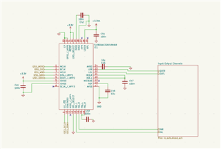
MCLK= 12.288MHz、fs = 48kHz、IOVDD = 3.3V、LDO_IN = 3.3V、AVdd = GND、 DVDD=GND、CM=0.75V

我成功通过 i2c 配置编解码器、但无法使编解码器回放 I2S。 我甚至无法在输出/输入引脚上测量配置的0.75V CM、因此我想编解码器未处于正确的配置中。

这是我当前的配置:

void codec_init(){
    /* ---------- switch to page 0 ---------- */
    codec_write_reg(0x00, 0x00);

    // software reset
    codec_write_reg(0x01, 0x01);

    /*---- Clock and Interface Settings ----*/
    // for Fs = 48KHz nad MCLK = 12.228MHz
    // Fs = MCLK/(NDAC * MDAC * OSR)
    // 48kHz = 12.288MHz/(1 * 2 * 128)


    // NDAC divider = 1
    codec_write_reg(0x0b, 0x81);
    // MDAC divider = 2
    codec_write_reg(0x0c, 0x82);

    // Power up NADC divider with value 1
    codec_write_reg(0x12, 0x81);

    // Power up MADC divider with value 2
    codec_write_reg(0x13, 0x82);
    
    // OSR of DAC = 128
    codec_write_reg(0x0d, 0x00);
    codec_write_reg(0x0e, 0x80);

    // OSR of ADC = 128
    codec_write_reg(0x14, 0x80);

    // set i2s mode
    // set word length/frame size to 32bit to send 24bit audio data
    // b00110000
    codec_write_reg(0x1b, 0x00);

    // set the DAC Mode to PRB_P8
    // codec_write_reg(0x3c, 0x08);

    // Select DAC PRB_P1
    codec_write_reg(0x3c, 0x01);

    // Select ADC PRB_R1
    codec_write_reg(0x3D, 0x01);

    // Select ADC PTM_R4
    codec_write_reg(0x3D, 0x00);

    // Set MicPGA startup delay to 3.1ms
    codec_write_reg(0x47, 0x32);


    /*---- Configure Power Supplies ----*/

    /* ---------- switch to page 1 ---------- */
    codec_write_reg(0x00, 0x01);

    // Disable weak AVDD-DVDD link     
    codec_write_reg(0x01, 0x08);

    // Power AVDD LDO
    codec_write_reg(0x02, 0x01);

    // set REF charging time to 40ms
    codec_write_reg(0x7b, 0x01);

    // HP soft stepping settings for optimal pop performance at power up
    // Rpop used is 6k with N = 6 and soft step = 20usec. This should work with 47uF coupling
    // capacitor. Can try N=5,6 or 7 time constants as well. Trade-off delay vs “pop” sound
    codec_write_reg(0x14, 0x25);

    // D7   = 0     reserved
    // D6   = 1     common mode to 0.75V
    // D4-5 = 00    Output Common Mode for HPL and HPR is same as full-chip common mode
    // D3   = 0     Output Common Mode for LOL and LOR is same as full-chip common mode
    // D2   = 0     reserved
    // D1   = 1     Power HP by LDOIN     
    // D0   = 1     LDOIN pin range 1.8V - 3.6V
    // 
    // 01000011 = 0x43
    codec_write_reg(0x0a, 0x43);

    /* ---- Routing ----*/

    // route dac to line outs
    // left channel
    codec_write_reg(0x0e, 0x08);
    // right channel
    codec_write_reg(0x0f, 0x08);

    // Route LINE_IN Left to LEFT_P with 20K input impedance
    codec_write_reg(0x34, 0x80);  
    // Route LINE_IN Right to RIGHT_P with 20K input impedance
    codec_write_reg(0x37, 0x80);  // Use appropriate register for LINE_IN routing
    

    // unmute line outs
    // LOL: unmute, 0 dB gain
    codec_write_reg(0x12, 0x00);
    // LOR: unmute, 0 dB gain
    codec_write_reg(0x13, 0x00);

    // Power up LOL and LOR drivers
	codec_write_reg(0x09, 0x3C);

    /* ---------- switch to page 0 ---------- */
    codec_write_reg(0x00, 0x00);

    // DACL DACR -> 0dB
    codec_write_reg(0x41, 0x00);
    codec_write_reg(0x42, 0x00);

    //  Power up the Left and Right DAC Channels with route the Left Audio digital data to
    // Left Channel DAC and Right Audio digital data to Right Channel DAC
    // 11010101
    codec_write_reg(0x3f, 0xd5);

    // unmute dac digital volume control
    codec_write_reg(0x40, 0x00);

    // Power up Left and Right ADC Channels
    // Do not use digital mic
    codec_write_reg(0x51, 0xF0);

    // Unmute Left and Right ADC Digital Volume Control
    codec_write_reg(0x52, 0x00);
}

也许关于输入级的另一个有趣的信息是:
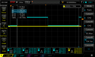
输入似乎处于悬空状态。 我的耦合电容器没有通过交流信号。 此外、我的运算放大器电路的作用类似于具有浮动输出(正弦信号失真到方波)。

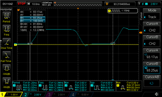
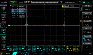
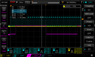
也许我的 MCLK 的信号完整性不是很完美、我会有一点过冲/下冲、但这应该起作用?
如果 MCLK 没有正确地为系统提供时钟、编解码器是否不会应用电源和路由配置?

感谢您的参与:>

  • 请注意,本文内容源自机器翻译,可能存在语法或其它翻译错误,仅供参考。如需获取准确内容,请参阅链接中的英语原文或自行翻译。

    您好、

    您能否附加原理图? 您目前有两条线路连接、但它们位于不同的 ADC 路径上、因此 ADC 的1/2输入保持悬空。 您至少需要使用寄存器0x36将 LEFT_M 连接到共模。 此外、我看到您没有取消输入 PGA 静音、对于左侧 PGA、可以使用页1寄存器0x3b 或右侧0x3c 来完成此操作。  

    以下是我在通读配置时做的一些其他注意事项:

    -寄存器0x1b 的长度应为0x30、长度为32位

    -注释输出或移动(0x3D、0x00);PTM 设置 位于第1页0x3D

    -注释出或移动(0x47, 0x32);这应该 在第1页改为(麦克风 PGA 设置)

    -第1页寄存器0x0a -确保 LDO 输入电压按照配置在1.8V 和3.6V 之间

    -将第0页寄存器0x51设置为0xc0而不是0xf0

    此致、
    Mir

  • 请注意,本文内容源自机器翻译,可能存在语法或其它翻译错误,仅供参考。如需获取准确内容,请参阅链接中的英语原文或自行翻译。

    感谢您的帮助! 我现在要查看配置。 根据您的回答、似乎我得到了一些主要的配置错误。 稍后我会报告是否能解决问题。

    一些便签:
    -我的 LDO 输入是3.3V
    -我切换到16位字长在我的 I2S 配置和忘记更改评论,所以这也是正确的。
    -我的寄存器0x51的配置是否会导致编解码器不工作,因为我使用了保留位?

    我对您的备注有几个问题:
    1. MICPGA 总是在 ADC 前面布线,即使我使用的是线路接口? 寄存器0x3B 如何使 PGA 静音? 在数据表的寄存器说明中:
    D7 0:启用左 MICPGA 增益
    1:左 MICPGA 增益设置为0dB、其中其复位值为1。

    这意味着复位后增益设置为0dB、这是正确的、因为我不想放大线路输入信号。 为什么我必须更改此寄存器 val、为什么默认值会使输入静音?

    2.我是否正确理解了这一点:由于 PGA 总是被迫在 ADC 前面,它的 CM 通过寄存器0x36路由是必不可少的,并且是在输入端路由 CM 的唯一方法?

    3.
    这是我的原理图:

    ADC IN 和 DAC OUT 引脚直接连接到耦合电容器。

    4.您能指出 DAC 为何不输出任何信号的错误吗? 我希望 MCLK 信号完整性可以很好地工作。 布线相当长、我没有使用端接电阻。

  • 请注意,本文内容源自机器翻译,可能存在语法或其它翻译错误,仅供参考。如需获取准确内容,请参阅链接中的英语原文或自行翻译。

    您好、

    如果配置0x51写入保留位、可能无法使器件完全停止工作、但最好不要写入保留位、因为可能会出现意外行为。 您可以将这些位保留为00 (默认值)、如果 ADC 未配置为数字麦克风、则任何配置为数字麦克风的输入都不会被使用。  

    1:抱歉、是的寄存器0x3b 不会使 PGA 静音-如果增益设置为0dB、则它会开启、或指定任何其他值。

    2:PGA 是 ADC 前面的级、需要一个 P 和一个 M 输入。 如果您打算使用两个单端输入(ADC 的每个通道上各一个)、则应将 M 输入连接到共模。

    3:我有一些关于电源去耦电容的注意事项:

    - DVDD 应该有10uf 和它有100nf (.1uf )
    - LDOIN 仅在需要100N、1uf 和10uf 并联时具有100N

    4:你在使用什么 BCLK? 1.536MHz? 您能否测量输入时钟和信号? 此外、让我知道、一旦您能够更改去耦电容器、这可能会影响器件的运行。  

    此致、
    Mir

  • 请注意,本文内容源自机器翻译,可能存在语法或其它翻译错误,仅供参考。如需获取准确内容,请参阅链接中的英语原文或自行翻译。

    感谢您的帮助、我正在更接近使其正常工作。

    一个输入通道现在正在工作、但实际上仅在正确的通道上工作。 左声道仍处于悬空状态。
    我可以通过 I2S 将样本读取到我的 rxBuffer 中。

    但我仍然无法从 DAC 输出数据。 我尝试实现一个简单的环回(将 rxBuffer 直接复制到 txBuffer 中)、但我无法使用输出引脚上的示波器来测量任何输出。

    我也不测量输出引脚上的 CM。 如果我认为正确配置 DAC、即使 I2S 连接出现故障、情况也应该是如此?

    这是我当前的配置:

    void codec_init(){
        /* ---------- switch to page 0 ---------- */
        codec_write_reg(0x00, 0x00);
    
        // software reset
        codec_write_reg(0x01, 0x01);
    
        /*---- Clock and Interface Settings ----*/
        // for Fs = 48KHz and MCLK = 12.288MHz
        // Fs = MCLK/(NDAC * MDAC * OSR)
        // 48kHz = 12.288MHz/(1 * 2 * 128)
    
        // NDAC divider = 1
        codec_write_reg(0x0b, 0x81);
        // MDAC divider = 2
        codec_write_reg(0x0c, 0x82);
    
        // Power up NADC divider with value 1
        codec_write_reg(0x12, 0x81);
    
        // Power up MADC divider with value 2
        codec_write_reg(0x13, 0x82);
        
        // OSR of DAC = 128
        codec_write_reg(0x0d, 0x00);
        codec_write_reg(0x0e, 0x80);
    
        // OSR of ADC = 128
        codec_write_reg(0x14, 0x80);
    
        // set i2s mode
        // set word length/frame size to 16bit
        codec_write_reg(0x1b, 0x00);
    
        // set the DAC Mode to PRB_P8
        // codec_write_reg(0x3c, 0x08);
        // Select DAC PRB_P1
        codec_write_reg(0x3c, 0x01);
    
        /*---- Configure Power Supplies ----*/
    
        /* ---------- switch to page 1 ---------- */
        codec_write_reg(0x00, 0x01);
    
        // Disable weak AVDD-DVDD link     
        codec_write_reg(0x01, 0x08);
    
        // Power AVDD LDO
        codec_write_reg(0x02, 0x01);
    
        // set REF charging time to 40ms
        codec_write_reg(0x7b, 0x01);
    
        // HP soft stepping settings for optimal pop performance at power up
        // Rpop used is 6k with N = 6 and soft step = 20usec. This should work with 47uF coupling
        // capacitor. Can try N=5,6 or 7 time constants as well. Trade-off delay vs “pop” sound
        codec_write_reg(0x14, 0x25);
    
        // D7   = 0     reserved
        // D6   = 1     common mode to 0.75V
        // D4-5 = 00    Output Common Mode for HPL and HPR is same as full-chip common mode
        // D3   = 0     Output Common Mode for LOL and LOR is same as full-chip common mode
        // D2   = 0     reserved
        // D1   = 1     Power HP by LDOIN     
        // D0   = 1     LDOIN pin range 1.8V - 3.6V
        // 
        // 01000011 = 0x43
        codec_write_reg(0x0a, 0x43);
    
        // Select ADC PRB_R1
        codec_write_reg(0x3D, 0x01);
    
        // Select ADC PTM_R4
        codec_write_reg(0x3D, 0x00);
    
        // Set MicPGA startup delay to 3.1ms
        codec_write_reg(0x47, 0x32);
        
        /* ---- Routing ----*/
    
        // route dac to line outs
        // left channel
        codec_write_reg(0x0e, 0x08);
        // right channel
        codec_write_reg(0x0f, 0x08);
    
        // Route LINE_IN Left to LEFT_P with 20K input impedance
        codec_write_reg(0x34, 0x80);  
        // Route Common Mode to LEFT_M with impedance of 20K
        codec_write_reg(0x36, 0x80);  
        // Route LINE_IN Right to RIGHT_P with 20K input impedance
        codec_write_reg(0x37, 0x80);
        // Route Common Mode to RIGHT_M with impedance of 20K
        codec_write_reg(0x39, 0x80);
    
        // unmute line outs
        // LOL: unmute, 0 dB gain
        codec_write_reg(0x12, 0x00);
        // LOR: unmute, 0 dB gain
        codec_write_reg(0x13, 0x00);
    
        // unmute left PGA
        codec_write_reg(0x3b, 0x00);
        // unmute right PGA
        codec_write_reg(0x3c, 0x00);
    
        // Power up LOL and LOR drivers
    	codec_write_reg(0x09, 0x3C);
    
        /* ---------- switch to page 0 ---------- */
        codec_write_reg(0x00, 0x00);
    
        // DACL DACR -> 0dB
        codec_write_reg(0x41, 0x00);
        codec_write_reg(0x42, 0x00);
    
        //  Power up the Left and Right DAC Channels with route the Left Audio digital data to
        // Left Channel DAC and Right Audio digital data to Right Channel DAC
        // 11010101
        codec_write_reg(0x3f, 0xd5);
    
        // unmute dac digital volume control
        codec_write_reg(0x40, 0x00);
    
        // Power up Left and Right ADC Channels
        // Do not use digital mic
        codec_write_reg(0x51, 0xc0);
    
        // Unmute Left and Right ADC Digital Volume Control
        codec_write_reg(0x52, 0x00);
    }

    感谢您的帮助!

    编辑:我使用的是12.288 MHz MCLK。 BCLK 和 WCLK 通过我的 STM32 HAL 自动派生。
    但我想这可以正常工作、因为我能够通过 I2S 读取数据(即使目前只有正确的通道)到我的 MCU 中。

  • 请注意,本文内容源自机器翻译,可能存在语法或其它翻译错误,仅供参考。如需获取准确内容,请参阅链接中的英语原文或自行翻译。

    您好、

    只有能够读取正确的频道似乎有趣... 通常、由于某些 BCLK 问题、我们会看到类似仅能够读取 I2S 的左通道。 但是、这仍然可能是时钟问题。 您能否在示波器上测量时钟? 如果处于16位模式 I2S、则每个 WCLK 应该有32个 BCLK 周期(BCLK 适用于两个通道 L+R)。 如果 WCLK 为48K、则 BCLK 将为1.536MHz。 可能 STM32的 BCLK 输出 不正确。

    要使 DAC 输出正常工作、您应将取消静音 LOL 和 LOR 线路移至 LOL 和 LOR 上电之后、如下所示:

    (0x3b, 0x00);// unmute left PGA
    (0x3c, 0x00);// unmute right PGA
    (0x09, 0x3C);// Power up LOL and LOR drivers
    (0x12, 0x00);// LOL: unmute, 0 dB gain
    (0x13, 0x00);// LOR: unmute, 0 dB gain

    另一个注意事项是数据表指定在 DAC 之前打开 ADC、因此您可能还需要更改脚本顺序的最后几行:
    (0x51, 0xc0);// Power up Left and Right ADC Channels
    (0x52, 0x00);// Unmute Left and Right ADC Digital Volume Control
    (0x3f, 0xd5);// power up dac
    (0x40, 0x00);// unmute dac digital volume control
    请告诉我您从中找到了什么。

    此致、
    Mir

  • 请注意,本文内容源自机器翻译,可能存在语法或其它翻译错误,仅供参考。如需获取准确内容,请参阅链接中的英语原文或自行翻译。

    我弄清楚左侧输入悬空的原因:我将其短接至 GND。 这是现在解决的,我感到尴尬...

    这些都是我时钟的测量值。 它们不是非常精确、但应在偏差限值范围内:

    在示波器屏幕截图中、您可以看到示波器频率测量以及我的手动光标测量。

    MCLK≈12.229MHz

    BCLK≈1.538Mhz

    WCLK≈47.98kHz

    WCLK+BCLK ->如您所见、WCLK 的一个周期恰好保持32个 BCLK 周期。


    关于缺少 DAC 输出、无法通过移动 DAC 上电的顺序并取消通道静音来解决该问题。 我仍然没有得到任何输出。

  • 请注意,本文内容源自机器翻译,可能存在语法或其它翻译错误,仅供参考。如需获取准确内容,请参阅链接中的英语原文或自行翻译。

    您好、

    很高兴输入现在起作用。 我 看到第1页 D3中的寄存器0x0a 设置为0、因此预计输出共模来自 AVDD 而不是 LDOIN -您是否可以将0x0a 设置为0x4b 而不是0x43? 否则、LOL+LOR 的输出由 AVDD 供电-使用 LDOIN 的原因是为了升高电势输出电压。 如果您不希望这样做、则需要将电源连接到 AVDD。 在更改该寄存器之前、您能否检查 HPL+HPR 引脚上是否存在共模输出?

    此致、
    Mir

  • 请注意,本文内容源自机器翻译,可能存在语法或其它翻译错误,仅供参考。如需获取准确内容,请参阅链接中的英语原文或自行翻译。

    1.尽管满芯片 CM 设置为0.75V、HPL HPR 测量值为960mV CM
    2.即使将0x0a 设置为0x4b、也无法在 LOL 或 LOR 上测量任何 CM。
    3、之后在 HPL 上看到 IN1L

    //将 IN1L 路由到 HPL
    codec_write_reg (0x0c、0x04);
    //取消 HPL 静音
    codec_write_reg (0x10、0x00);

    但我想这并没有证明什么、因为它仅进行模拟布线。

    4、HPL 上没有输出可以测量,何时测量

    //将左 DAC 路由到 HPL
    codec_write_reg (0x0c、0x08);
    //取消 HPL 静音
    codec_write_reg (0x10、0x00);

    //为混频器、LOL 和 LOR 以及 HPL 驱动器加电
    codec_write_reg (0x09、0x3f);

    我的计划是使用 LDOIN 完全生成我的 CM。 我的电路中未连接 AVDD。

  • 请注意,本文内容源自机器翻译,可能存在语法或其它翻译错误,仅供参考。如需获取准确内容,请参阅链接中的英语原文或自行翻译。

    您好、

    刚刚意识到、您在第1页的寄存器0x02中缺少了"模拟块功耗"。 您应该将其设置为0x09而不是0x01。

    请告诉我、当您切换时会发生什么情况。  

    此致、
    Mir