This thread has been locked.

If you have a related question, please click the "Ask a related question" button in the top right corner. The newly created question will be automatically linked to this question.

[参考译文] LAUNCHXL-F28379D:运行调试器时 TMS320F28379D 挂起 — 如果阵列大小很小则可以

Guru**** 2533760 points
Other Parts Discussed in Thread: C2000WARE

请注意,本文内容源自机器翻译,可能存在语法或其它翻译错误,仅供参考。如需获取准确内容,请参阅链接中的英语原文或自行翻译。

https://e2e.ti.com/support/microcontrollers/c2000-microcontrollers-group/c2000/f/c2000-microcontrollers-forum/1564144/launchxl-f28379d-tms320f28379d-hangs-when-running-the-debugger----ok-if-array-size-is-small

器件型号:LAUNCHXL-F28379D
主题:C2000WARE 中讨论的其他器件

工具/软件:

您好:

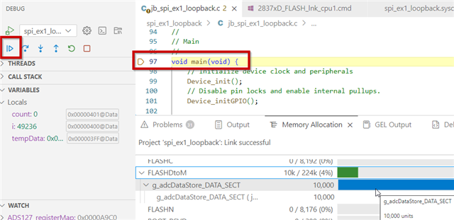
我需要在闪存中存储一个大型阵列、但我发现调试器永远不会达到初始化状态、在初始化状态下、您点击“Continue"蓝色“蓝色按钮。 同样的故事,直接编程的闪存,它没有经历。

例如、工作原理如下:

const uint32_t g_adcDataStoreSize = 10e3
#pragma DATA_SECTION (g_adcDataStore“g_adcDataStore_data_sect")“)
uint16_t g_adcDataStore[g_adcDataStoreSize]={0};
 

很好!

~~~~~~~~~~~~~μ s

这不奏效:

const uint32_t g_adcDataStoreSize = 100e3
#pragma DATA_SECTION (g_adcDataStore“g_adcDataStore_data_sect")“)
uint16_t g_adcDataStore[g_adcDataStoreSize]={0};

糟糕!

我一直不会点击“Resume"按钮“按钮、并且代码无法运行。 我知道闪存没有正确写入、因为我有一个 GPIO 引脚设置为高电平作为测试。

您可以在图片中看到、闪存中有足够的空间、也没有构建错误。

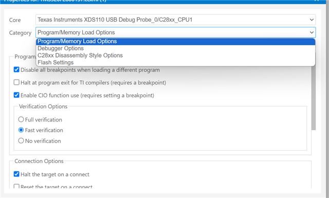
我的.cmd 文件中是否有不正确的内容? 还有其他问题吗?

.cmd 文件:

e2e.ti.com/.../2860.2837xD_5F00_FLASH_5F00_lnk_5F00_cpu1.cmd

.c 文件:

e2e.ti.com/.../jb_5F00_spi_5F00_ex1_5F00_loopback.c

我期待你们的支持。

请注意、

Jennifer

应用工程师

时钟和计时解决方案

  • 请注意,本文内容源自机器翻译,可能存在语法或其它翻译错误,仅供参考。如需获取准确内容,请参阅链接中的英语原文或自行翻译。

    您好、是否对此进行了任何更新?

  • 请注意,本文内容源自机器翻译,可能存在语法或其它翻译错误,仅供参考。如需获取准确内容,请参阅链接中的英语原文或自行翻译。

    Jennifer

    很抱歉在响应此主题时出现延迟。  

    请澄清以下问题、这些问题可能有助于缩小此问题的原因范围

    1.是否可以共享在编译大数组后生成的.map 文件?

    2.闪存操作期间显示的错误是什么? 它是刚刚挂起还是您在控制台输出窗口中看到任何输出?

    3.您可以在 Flash 设置下启用“详细输出“选项,查看是否抛出任何错误
    您可以通过在调试器视图的“线程“部分下右键点击已连接的内核来启用此功能、浏览到 Properties、然后选择“Flash settings“选项、然后向下滚动以启用 Verbose 输出选项  


    此致

    Siddharth

  • 请注意,本文内容源自机器翻译,可能存在语法或其它翻译错误,仅供参考。如需获取准确内容,请参阅链接中的英语原文或自行翻译。

    您好、Siddharth

    我真的很感谢支持、因为这是我的测试的关键。

    1.这里是清理后再重建的映射文件。

    e2e.ti.com/.../spi_5F00_ex1_5F00_loopback.map

    2.在“Output",“,"GEL、"GEL Output"“ Output",“,"CIO"、"CIO"和“和"Debug“"Debug Console"“ Console"窗口“窗口中未观察到任何文本。 在“Debug Output“窗口中未观察到可见错误。

    3.启用 verbose 后的“Debug Output“窗口:

    C28xx_CPU1: If erase/program (E/P) operation is being done on one core, the other core should not execute from shared-RAM (SR) as they are used for the E/P code. Also, CPU1 will be halted to determine SR ownership for the CPU which will run the Flash Plugin code, after which CPU1 will be set to run its application. User code execution from SR could commence after the selected flash banks are programmed.
    C28xx_CPU1: Writing Flash @ Address 0x00080000 of Length 0x00000002 (page 0)
    C28xx_CPU1: PLL configuration status = 1. PLL configured successfully.
    C28xx_CPU1: Erasing Flash Bank 0, Sector A
    C28xx_CPU1: Erasing Flash Bank 0, Sector B
    C28xx_CPU1: Erasing Flash Bank 0, Sector C
    C28xx_CPU1: Erasing Flash Bank 0, Sector D
    C28xx_CPU1: Erasing Flash Bank 0, Sector E
    C28xx_CPU1: Erasing Flash Bank 0, Sector F
    C28xx_CPU1: Erasing Flash Bank 0, Sector G
    C28xx_CPU1: Erasing Flash Bank 0, Sector H
    C28xx_CPU1: Erasing Flash Bank 0, Sector I
    C28xx_CPU1: Erasing Flash Bank 0, Sector J
    C28xx_CPU1: Erasing Flash Bank 0, Sector K
    C28xx_CPU1: Erasing Flash Bank 0, Sector L
    C28xx_CPU1: Erasing Flash Bank 0, Sector M
    C28xx_CPU1: Erasing Flash Bank 0, Sector N
    C28xx_CPU1: Data has been buffered at the end of the current data block for 64-bit aligned writes.
    C28xx_CPU1: Writing Flash @ Address 0x00080008 of Length 0x00000128 (page 0)
    C28xx_CPU1: Verifying Flash @ Address 0x00080008 of Length 0x00000250
    C28xx_CPU1: Writing Flash @ Address 0x00080130 of Length 0x0000094e (page 0)
    C28xx_CPU1: Data has been buffered at the end of the current data block for 64-bit aligned writes.
    C28xx_CPU1: Verifying Flash @ Address 0x00080130 of Length 0x00001298
    C28xx_CPU1: Writing Flash @ Address 0x00080a80 of Length 0x00002852 (page 0)
    C28xx_CPU1: Data has been buffered at the end of the current data block for 64-bit aligned writes.
    C28xx_CPU1: Verifying Flash @ Address 0x00080A80 of Length 0x00004000
    C28xx_CPU1: Verifying Flash @ Address 0x00082A80 of Length 0x000010A0
    C28xx_CPU1: Writing Flash @ Address 0x000832d8 of Length 0x00000052 (page 0)
    C28xx_CPU1: Data has been buffered at the end of the current data block for 64-bit aligned writes.
    C28xx_CPU1: Verifying Flash @ Address 0x000832D8 of Length 0x000000A0
    C28xx_CPU1: Writing buffered data @ Address 0x00080000 of Length 0x00000004
    C28xx_CPU1: Verifying Flash @ Address 0x00080000 of Length 0x00000008
    C28xx_CPU1: Writing buffered data @ Address 0x00080A7C of Length 0x00000004
    C28xx_CPU1: Verifying Flash @ Address 0x00080A7C of Length 0x00000008
    C28xx_CPU1: Writing buffered data @ Address 0x000832D0 of Length 0x00000004
    C28xx_CPU1: Verifying Flash @ Address 0x000832D0 of Length 0x00000008
    C28xx_CPU1: Writing buffered data @ Address 0x00083328 of Length 0x00000004
    C28xx_CPU1: Verifying Flash @ Address 0x00083328 of Length 0x00000008

    它只是挂起:

    您看到了什么问题吗?

    感谢您发送编修。

    Jennifer

  • 请注意,本文内容源自机器翻译,可能存在语法或其它翻译错误,仅供参考。如需获取准确内容,请参阅链接中的英语原文或自行翻译。

    Jennifer

    请告诉我您使用的是哪个版本的 CCS 和 C2000Ware?  此外、为什么您打算将该数组存储在闪存而不是 RAM 中?  

    我尝试在其中一个项目中执行类似的操作、但没有遇到此错误。

    C28xx_CPU1: Writing Flash @ Address 0x00080000 of Length 0x00000002 (page 0)
    C28xx_CPU1: PLL configuration status = 1. PLL configured successfully.
    C28xx_CPU1: Erasing Flash Bank 0, Sector A
    C28xx_CPU1: Erasing Flash Bank 0, Sector B
    C28xx_CPU1: Erasing Flash Bank 0, Sector C
    C28xx_CPU1: Erasing Flash Bank 0, Sector D
    C28xx_CPU1: Erasing Flash Bank 0, Sector E
    C28xx_CPU1: Erasing Flash Bank 0, Sector F
    C28xx_CPU1: Erasing Flash Bank 0, Sector G
    C28xx_CPU1: Erasing Flash Bank 0, Sector H
    C28xx_CPU1: Erasing Flash Bank 0, Sector I
    C28xx_CPU1: Erasing Flash Bank 0, Sector J
    C28xx_CPU1: Erasing Flash Bank 0, Sector K
    C28xx_CPU1: Erasing Flash Bank 0, Sector L
    C28xx_CPU1: Erasing Flash Bank 0, Sector M
    C28xx_CPU1: Erasing Flash Bank 0, Sector N
    C28xx_CPU1: Data has been buffered at the end of the current data block for 64-bit aligned writes.
    C28xx_CPU1: Writing Flash @ Address 0x00082000 of Length 0x0000170a (page 0)
    C28xx_CPU1: Data has been buffered at the end of the current data block for 64-bit aligned writes.
    C28xx_CPU1: Verifying Flash @ Address 0x00082000 of Length 0x00002E10
    C28xx_CPU1: Writing Flash @ Address 0x00084000 of Length 0x000003f3 (page 0)
    C28xx_CPU1: Data has been buffered at the end of the current data block for 64-bit aligned writes.
    C28xx_CPU1: Verifying Flash @ Address 0x00084000 of Length 0x000007E0
    C28xx_CPU1: Writing Flash @ Address 0x000843f8 of Length 0x00000128 (page 0)
    C28xx_CPU1: Verifying Flash @ Address 0x000843F8 of Length 0x00000250
    C28xx_CPU1: Writing buffered data @ Address 0x00080000 of Length 0x00000004
    C28xx_CPU1: Verifying Flash @ Address 0x00080000 of Length 0x00000008
    C28xx_CPU1: Writing buffered data @ Address 0x00083708 of Length 0x00000004
    C28xx_CPU1: Verifying Flash @ Address 0x00083708 of Length 0x00000008
    C28xx_CPU1: Writing buffered data @ Address 0x000843F0 of Length 0x00000004
    C28xx_CPU1: Verifying Flash @ Address 0x000843F0 of Length 0x00000008

      此致

    Siddharth