

请注意,本文内容源自机器翻译,可能存在语法或其它翻译错误,仅供参考。如需获取准确内容,请参阅链接中的英语原文或自行翻译。
器件型号:TMS320F28P650DK工具/软件:
尊敬的 Champs:
我使用 F28P65 LaunchPad 和 CCS12.8.1 进行测试。
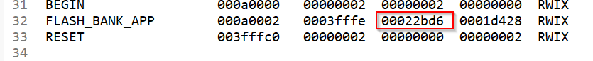
我在.cmd 文件中将闪存组 1 和 2 定义为 FLASH_BANK_APP、并使用它们。 在我的代码中、我将所有闪存存储体都分配给了 CPU1。
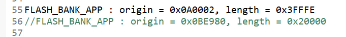
当我的闪存中的代码小于 0x20000 时、我的代码全部存储在闪存组 1 中、并且可以正常编程。 但是、一旦代码大小大于 0x20000、即代码需要存储在闪存组 1 和 2 中、我的编程将失败、错误消息如下所示:
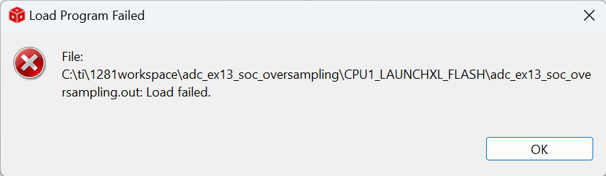
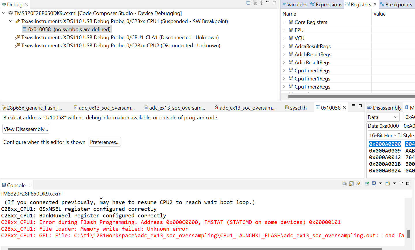
“Console"窗口“窗口显示:
C28xx_CPU1: GEL Output:
Memory Map Initialization Complete
C28xx_CPU1: GEL Output: ... DCSM Initialization Start ...
C28xx_CPU1: GEL Output: ... DCSM Initialization Done ...
C28xx_CPU1: GEL Output:
 CPU2 is out of reset and configured to wait boot.
 (If you connected previously, may have to resume CPU2 to reach wait boot loop.)
C28xx_CPU1: If erase/program (E/P) operation is being done on one core, the other core should not execute from shared-RAM (SR) as they are used for the E/P code. User code execution from SR could commence after the selected flash banks are programmed.
C28xx_CPU1: Only CPU1 on-chip Flash Plugin can configure clock for CPU1, and CPU2 Flash operations. Plugin automatically configures PLL when CPU1 Flash operations are invoked. However, if users want to do only CPU2 Flash operations without doing a prior CPU1 operation in the current session, they should click on 'Configure Clock' button in CPU1's on-chip Flash Plugin before invoking CPU2 Flash operations. When this button is used, Flash Plugin will configure the clock for CPU1/CPU2 at 200MHz using INTOSC as the clock source. Plugin will leave PLL config like this and user application should configure the PLL as required by application.
C28xx_CPU1: Before doing any flash operations using the flash plugin, (a) Please select which flash banks should be mapped to which CPU (CPU1 vs CPU2) - This selection should be done in CPU1 flash plugin GUI. (b) Please select the flash banks that the user would like the flash plugin to erase (in the CPU1 flash plugin GUI and the CPU2 flash plugin GUI)
C28xx_CPU1: GEL Output: ... DCSM Initialization Start ...
C28xx_CPU1: GEL Output: ... DCSM Initialization Done ...
C28xx_CPU1: GEL Output:
 CPU2 is out of reset and configured to wait boot.
 (If you connected previously, may have to resume CPU2 to reach wait boot loop.)
C28xx_CPU1: GEL Output: ... DCSM Initialization Start ...
C28xx_CPU1: GEL Output: ... DCSM Initialization Done ...
C28xx_CPU1: GEL Output:
 CPU2 is out of reset and configured to wait boot.
 (If you connected previously, may have to resume CPU2 to reach wait boot loop.)
C28xx_CPU1: GEL Output: ... DCSM Initialization Start ...
C28xx_CPU1: GEL Output: ... DCSM Initialization Done ...
C28xx_CPU1: GEL Output:
 CPU2 is out of reset and configured to wait boot.
 (If you connected previously, may have to resume CPU2 to reach wait boot loop.)
C28xx_CPU1: GSxMSEL register configured correctly
C28xx_CPU1: BankMuxSel register configured correctly
C28xx_CPU1: Error during Flash Programming. Address 0x000C0000, FMSTAT (STATCMD on some devices) 0x00000101
C28xx_CPU1: File Loader: Memory write failed: Unknown error
C28xx_CPU1: GEL: File: C:\ti\1281workspace\adc_ex13_soc_oversampling\CPU1_LAUNCHXL_FLASH\adc_ex13_soc_oversampling.out: Load failed.
您可以直接使用下面的项目重现此问题、 我在项目中使用了大量重复的代码、这增加了闪存代码的大小。
e2e.ti.com/.../adc_5F00_ex13_5F00_soc_5F00_oversampling.zip
谢谢!
此致、
Julia


