

Other Parts Discussed in Thread: TMS320F280025C
请注意,本文内容源自机器翻译,可能存在语法或其它翻译错误,仅供参考。如需获取准确内容,请参阅链接中的英语原文或自行翻译。
器件型号: TMS320F280025C
大家好:
我正在努力实现 TMS320F280025C 。
我想 使用 RS485 将数据阵列从 Docklight 传输到控制器 。
数据数组如下所示:
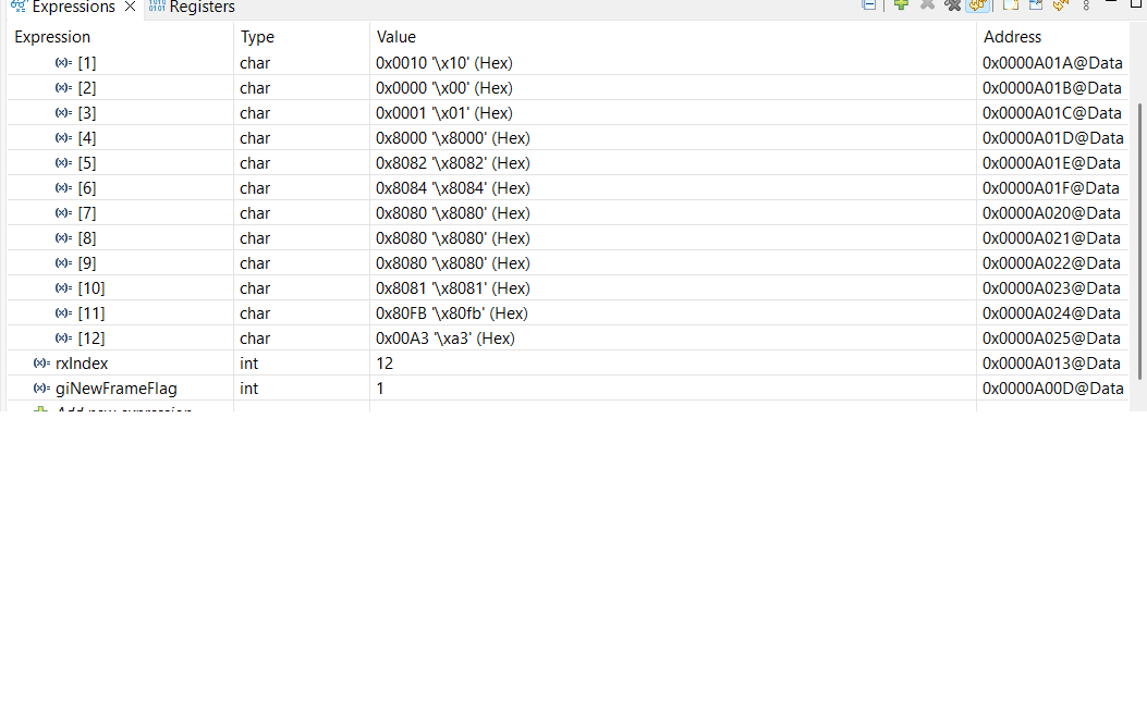
01 10 00 01 00 02 04 00 00 00 01 F3 A3
在控制器上收到此数据时、我遇到了以下问题:
-
有时是 正确接收整个数据帧
-
有时会收到数据 如随附的屏幕截图所示 (损坏的数据)
-
有时数据是正确的 只是缺少最后一个字节
我在下面分享我的代码。
请 查看代码、帮助我了解出现此问题的原因 。
波特率为 9600……
#include "F28x_Project.h"
#include "extern.h"
#include <stdint.h>

// Function Prototypes
void initSCIAEchoback(void);
void transmitSCIAChar(uint16_t a);
void transmitSCIAMessage(unsigned char * msg);
void initSCIAFIFO(void);
interrupt void sciaRxFifoIsr(void);

int a;
// Main
void main(void)
{
    // Initialize device clock and peripherals
    InitSysCtrl();

    // Initialize GPIO
    InitGpio();

    // For this example, only init the pins for the SCI-A port.
    // GPIO_SetupPinMux() - Sets the GPxMUX1/2 and GPyMUX1/2 register bits
    // GPIO_SetupPinOptions() - Sets the direction and configuration of GPIOs
    // These functions are found in the F28X7x_Gpio.c file.
    GPIO_SetupPinMux(3, GPIO_MUX_CPU1, 9);   // see datasheet page no.40... 9 is depend on that chart
    GPIO_SetupPinOptions(3, GPIO_INPUT, GPIO_PULLUP);
    GPIO_SetupPinMux(2, GPIO_MUX_CPU1, 9);
    GPIO_SetupPinOptions(2, GPIO_OUTPUT, GPIO_ASYNC);

    GPIO_SetupPinMux(7, GPIO_MUX_CPU1, 0);
    GPIO_SetupPinOptions(7, GPIO_OUTPUT, GPIO_PUSHPULL);

    // Disable CPU interrupts
    DINT;

    // Initialize the PIE control registers to their default state.
    // The default state is all PIE interrupts disabled and flags
    // are cleared.
    InitPieCtrl();

    // Disable CPU interrupts and clear all CPU interrupt flags
    IER = 0x0000;
    IFR = 0x0000;

    // Initialize the PIE vector table with pointers to the shell Interrupt
    // Service Routines (ISR)
    InitPieVectTable();

    // Interrupts that are used in this example are re-mapped to
    // ISR functions found within this file.
    EALLOW;  // This is needed to write to EALLOW protected registers
    PieVectTable.SCIA_RX_INT = &sciaRxFifoIsr;
    EDIS;    // This is needed to disable write to EALLOW protected registers

    // Enable global Interrupts and higher priority real-time debug events:
    IER = M_INT9 ;                        // For ADCA0,EPWM1 and for SCIC_RX

    // Enable interrupts for SCI/UART required for this example
    PieCtrlRegs.PIECTRL.bit.ENPIE = 1;   // Enable the PIE block
    PieCtrlRegs.PIEIER9.bit.INTx1 = 1;   // PIE Group 9, INT1  SCI RX.. see page no. 96

    initSCIAEchoback();                    // Initialize SCI for echoback

    GPIO_WritePin(7, 0);   // RS485 receive
    DELAY_US(1000);

    EINT;                                  // Enable Global interrupt INTM
    ERTM;                                  // Enable Global real-time interrupt DBGM

    for(;;)
    {
//       modbus();
//       while (SciaRegs.SCIFFTX.bit.TXFFST != 0) {}
//       SciaRegs.SCITXBUF.all = 0xD7;
//
//       DELAY_US(1000*1000);         // 1s
//       loopCounter++;
    }
}

//  initSCIAEchoback - Initialize SCI-A for echo-back
void initSCIAEchoback(void)
{
    SciaRegs.SCICCR.all = 0x0007;           // 1 stop bit,  No loopback
                                            // No parity, 8 char bits,
                                            // async mode, idle-line protocol
    SciaRegs.SCICTL1.all = 0x0003;          // enable TX, RX, internal SCICLK,
                                            // Disable RX ERR, SLEEP, TXWAKE
    SciaRegs.SCICTL2.all = 0x0003;
    SciaRegs.SCICTL2.bit.RXBKINTENA = 1;

    // SCIA at 9600 baud
    // @LSPCLK = 25 MHz (100 MHz SYSCLK) HBAUD = 0x01  and LBAUD = 0x44.
    SciaRegs.SCIHBAUD.all = 0x0001;
    SciaRegs.SCILBAUD.all = 0x0044;

    SciaRegs.SCIFFTX.all = 0xE040;
    SciaRegs.SCIFFRX.all = 0x0022;
    SciaRegs.SCIFFCT.all = 0x0;

    SciaRegs.SCIFFRX.bit.RXFIFORESET = 1;

    SciaRegs.SCICTL1.all = 0x0023;          // Relinquish SCI from Reset
}

// scicRxFifoIsr - Scic Receive FIFO ISR
interrupt void sciaRxFifoIsr(void)
{
    // Wait for incoming character
  //  while(SciaRegs.SCIFFRX.bit.RXFFST == 0) {}  //wait for empty state
    // Get character
    rxBuffer[rxIndex++] = (uint16_t)(SciaRegs.SCIRXBUF.all & 0x00FF);

    if (rxIndex==13)
    {
        GPIO_WritePin(7, 0);  // RX mode
        DELAY_US(20);
        rxIndex=0;
        giNewFrameFlag=1;
        a++;
    }

    SciaRegs.SCIFFRX.bit.RXFFOVRCLR=1;   // Clear Overflow flag
    SciaRegs.SCIFFRX.bit.RXFFINTCLR=1;   // Clear Interrupt flag

    PieCtrlRegs.PIEACK.all|=M_INT9;       // Issue PIE ack
}
