Other Parts Discussed in Thread: SYSCONFIG
器件型号: TMS320F28P650DK
主题: SysConfig 中讨论的其他器件
您好:
F28P650DK 微控制器提供了一个午餐板。
我想运行一个使用 SysConfig 工具配置的多核示例工程。 在本例中、工程是“led_ex2_blinky_sysconfig"工程“工程。
按下“Debug"按钮“按钮时会遇到以下问题:
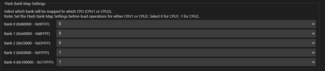
C28xx_CPU1: GEL Output: Memory Map Initialization CompleteC28xx_CPU1: GEL Output: ... DCSM Initialization Start ... C28xx_CPU1: GEL Output: ... DCSM Initialization Done ...C28xx_CPU1: GEL Output: CPU2 is out of reset and configured to wait boot. (If you connected previously, may have to resume CPU2 to reach wait boot loop.)C28xx_CPU1: If erase/program (E/P) operation is being done on one core, the other core should not execute from shared-RAM (SR) as they are used for the E/P code. User code execution from SR could commence after the selected flash banks are programmed.C28xx_CPU1: Only CPU1 on-chip Flash Plugin can configure clock for CPU1, and CPU2 Flash operations. Plugin automatically configures PLL when CPU1 Flash operations are invoked. However, if users want to do only CPU2 Flash operations without doing a prior CPU1 operation in the current session, they should click on 'Configure Clock' button in CPU1's on-chip Flash Plugin before invoking CPU2 Flash operations. When this button is used, Flash Plugin will configure the clock for CPU1/CPU2 at 200MHz using INTOSC as the clock source. Plugin will leave PLL config like this and user application should configure the PLL as required by application.C28xx_CPU1: Before doing any flash operations using the flash plugin, (a) Please select which flash banks should be mapped to which CPU (CPU1 vs CPU2) - This selection should be done in CPU1 flash plugin GUI. (b) Please select the flash banks that the user would like the flash plugin to erase (in the CPU1 flash plugin GUI and the CPU2 flash plugin GUI)C28xx_CPU1: GEL Output: ... DCSM Initialization Start ... C28xx_CPU1: GEL Output: ... DCSM Initialization Done ...C28xx_CPU1: GEL Output: CPU2 is out of reset and configured to wait boot. (If you connected previously, may have to resume CPU2 to reach wait boot loop.)C28xx_CPU1: GEL Output: ... DCSM Initialization Start ... C28xx_CPU1: GEL Output: ... DCSM Initialization Done ...C28xx_CPU1: GEL Output: CPU2 is out of reset and configured to wait boot. (If you connected previously, may have to resume CPU2 to reach wait boot loop.)C28xx_CPU1: GSxMSEL register configured correctlyC28xx_CPU1: BankMuxSel register configured correctlyC28xx_CPU2: GEL Output:
RAM initialization done
C28xx_CPU2: GEL Output: Memory Map Initialization CompleteC28xx_CPU2: If erase/program (E/P) operation is being done on one core, the other core should not execute from shared-RAM (SR) as they are used for the E/P code. User code execution from SR could commence after the selected flash banks are programmed.C28xx_CPU2: Only CPU1 on-chip Flash Plugin can configure clock for CPU1, and CPU2 Flash operations. Plugin automatically configures PLL when CPU1 Flash operations are invoked. However, if users want to do only CPU2 Flash operations without doing a prior CPU1 operation in the current session, they should click on 'Configure Clock' button in CPU1's on-chip Flash Plugin before invoking CPU2 Flash operations. When this button is used, Flash Plugin will configure the clock for CPU1/CPU2 at 200MHz using INTOSC as the clock source. Plugin will leave PLL config like this and user application should configure the PLL as required by application.C28xx_CPU2: Before doing any flash operations using the flash plugin, (a) Please select which flash banks should be mapped to which CPU (CPU1 vs CPU2) - This selection should be done in CPU1 flash plugin GUI. (b) Please select the flash banks that the user would like the flash plugin to erase (in the CPU1 flash plugin GUI and the CPU2 flash plugin GUI)C28xx_CPU2: GSxMSEL register configured correctlyC28xx_CPU2: Flash Programmer: Error erasing Bank 0 FMSTAT (STATCMD on some devices) value = 65 (decimal). Operation Cancelled (0).C28xx_CPU2: File Loader: Memory write failed: Unknown errorC28xx_CPU2: GEL: File: C:\Users\jsola\workspace_v12\led_ex2_blinky_sysconfig_cpu1\FLASH\led_ex2_blinky_sysconfig_cpu1.out: Load failed.
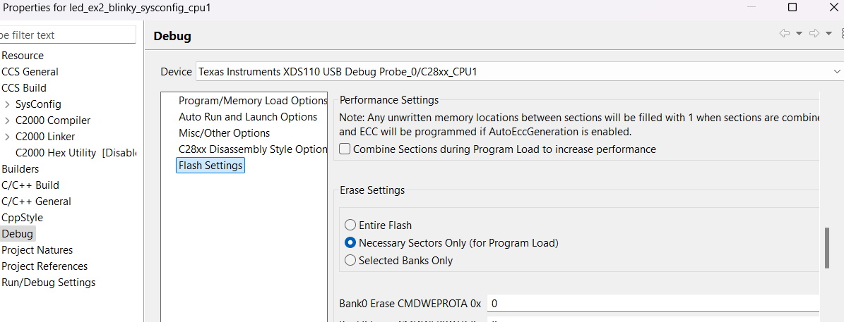
我尝试搜索并修改了每个工程中的闪存设置、以便仅擦除必要的闪存组。 这是 CPU1 中工程的配置:
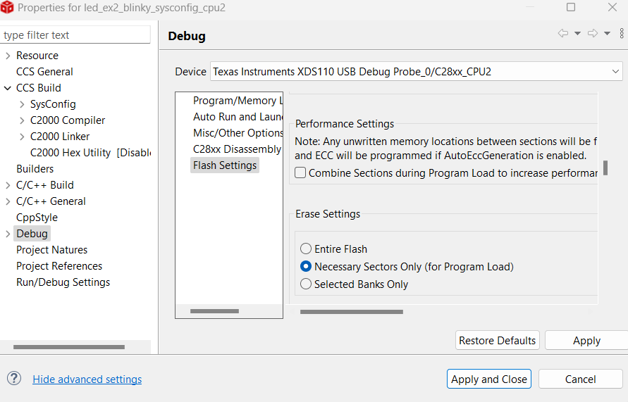
以下是 CPU2 中工程的配置:
为什么我仍然收到该错误、可以采取什么措施来解决该错误?
谢谢你。