Other Parts Discussed in Thread: ADS1261
请注意,本文内容源自机器翻译,可能存在语法或其它翻译错误,仅供参考。如需获取准确内容,请参阅链接中的英语原文或自行翻译。
器件型号:TMS320F280045 主题中讨论的其他器件:ADS1261
尊敬的 Sirs
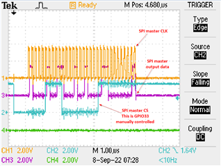
我使用 F280045_56RSH uC 来控制 ADS1261 ADC。 由于路由问题、无法 使用正常的 SPIA CS。 我将在"use"中为 SPIA 主器件使用"custom"设置 、为 CS 使用 GPIO33引脚29、该引脚由手动控制。 所有这些都在 .syscfg GUI 中进行配置。 请参阅下面的 syscfg GUI、代码和示波器图像。 我将发送4个字节的数据、每个 CS 周期2个字节。 CS 按预期变低、请参阅下面的示波器捕获。 但是、我注意到了两件事。 首先、4个字节之间不会以任何时间延迟分隔、它们是连续的。 我本想每个字节之间会有一些时间。 其次、会生成两个 CS、但它们是溢出的。 请帮助解决这些问题。 谢谢你。

//
// This function performs the basic ADC initialization.
//
void ADC_init(void)
{
    ADC_RST();
    //
    // Write the MODE0 register
    // Set the sample rate to 7200SPS and the filter to SINC3.
    // (MODE0_DR_7200_SPS | MODE0_SINC3) = 0x62
    //
    ADC_Write_Reg(REG_ADDR_MODE0, (MODE0_DR_7200_SPS | MODE0_SINC3));

    //
    // Write the MODE1 register
    // Set the conversion start delay to 50us, chop mode to off and convertion mode to continuous.
    // (MODE1_DELAY_50_uST | MODE1_CHOP_OFF | MODE1_CONVRT_CONTINUOUS) = 0x01
    //
    ADC_Write_Reg(REG_ADDR_MODE1, (MODE1_DELAY_50_uS | MODE1_CHOP_OFF | MODE1_CONVRT_CONTINUOUS));

    //
    // Write the MODE2 register
    // Enables AIN2 and AIN3 as outputs.
    // Connect AIN2 to GPIO0 and AIN3 to GPIO1
    // These IOs control the bridge excitation direction switches.
    // (MODE2_GPIOCON_AIN3_ENABLE_MASK | MODE2_GPIOCON_AIN2_ENABLE_MASK) = 0x30
    //
    ADC_Write_Reg(REG_ADDR_MODE2, (MODE2_GPIOCON_AIN3_ENABLE_MASK | MODE2_GPIOCON_AIN2_ENABLE_MASK));

    //
    // Write the MODE3 register
    // Set AIN3's output to high. AIN2's output is default low.
    // MODE3_GPIODAT_AIN3_DATA_MASK = 0x02
    //
    ADC_Write_Reg( REG_ADDR_MODE3, MODE3_GPIODAT_AIN3_DATA_MASK);

    //
    // Write the REF register
    // Enable the internal reference to enable the internal current source to be used.
    // NOTE: any time the REF register is changed, REF_REFENB_MASK must be ORed with the change
    // in order to maintain the IDAC1 current output.
    // (REF_REFENB_MASK | REF_RMUXP_AVDD | REF_RMUXN_AVSS) = 0x15
    //
    ADC_Write_Reg(REG_ADDR_REF, (REF_REFENB_MASK | REF_RMUXP_AVDD | REF_RMUXN_AVSS));

    //
    // Write the IMUX1 and IMUX2 registers
    // Select IDAC1 and IDAC2 to be connected to AINCOM.
    // (IMUX_IMUX2_NOCONNECT | IMUX_IMUX1_AINCOM) = 0xFA
    //
    ADC_Write_Reg(REG_ADDR_IMUX, (IMUX_IMUX2_AINCOM | IMUX_IMUX1_AINCOM));

    //
    // Write the IMAG register
    // Set IDAC1 output to 500uA and IDAC2 to 100uA
    // (IMAG_IMAG2_100_uA | IMAG_IMAG1_500_uA) = 0x24
    // NOTE: The excitation current is set to 600uA to ensure that the voltage
    // at the current output pin does not exceed the 3.9V limit for a maximum
    // bridge resistance of 6350 ohm @ 50°C.
    //
    ADC_Write_Reg(REG_ADDR_IMAG, (IMAG_IMAG2_100_uA | IMAG_IMAG1_500_uA));
}
//
// This function writes to the designated ADC register.
//
void ADC_Write_Reg(uint8_t reg_addr, uint8_t reg_data)
{
    uint16_t tempData;
    uint16_t shifted_RegAddr;
    uint16_t shifted_Data;

    shifted_RegAddr = ((OPCODE_WREG + reg_addr) << 8);          // OPCODE_WREG is defined as 0x40
    shifted_Data = reg_data << 8;

    tempData = SPI_readDataNonBlocking(SPIA_BASE);              // Empty the receive register.
    ADC_CS(LOW);                                                // Enable CS for the ADC.
    SPI_writeDataBlockingNonFIFO(SPIA_BASE, shifted_RegAddr);   // Send write command (0x40) to ADS1261.
    tempData = SPI_readDataNonBlocking(SPIA_BASE);              // Empty the receive register.
    SPI_writeDataBlockingNonFIFO(SPIA_BASE, shifted_Data);      // Send out the data to ADS1261.
    tempData = SPI_readDataNonBlocking(SPIA_BASE);              // Empty the receive register.
    ADC_CS(HIGH);                                               // Disable CS for the ADC.

}