请注意,本文内容源自机器翻译,可能存在语法或其它翻译错误,仅供参考。如需获取准确内容,请参阅链接中的英语原文或自行翻译。
器件型号:TMS320F280025C 您好!
我的比较器子系统(CMPSS)有问题、我已使用 CMP1_HP2和 CMP1_LP3为 CMPSS1配置一个输入信号、每个比较器具有两个不同的 DAC 阈值。 我想在事件发生时触发中断,当我在内部创建断点时,代码停止,所以检测正常,COMPSTS 正常。
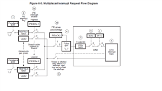
稍后、我必须配置另外两个比较器、我想在中断中检测哪个比较器是通过 COMPSTS.bit.COMPHSTS 触发的、哪个比较器是通过另一个比较器的 COMPLSTS 触发的。 在中断中、DCBEVT2事件的清零不起作用、中断的 INT 位为什么不起作用?
在不更改比较器输入端的电压电平的同时将断点留在中断中的情况下、我进行两次循环、然后在中断中不再返回任何值、原因是什么? 但是、我通过 PieCtrlRegs.PIEACK.bit.ACK2 = 1来确认中断
#include "f28002x_device.h"
#include "HPTS100_tripzone.h"
#include "f28002x_examples.h"

bool test;
__interrupt void tripzone_isr(void)
{
    test = true;
    /// For MU_TRAC_BATT_PCH Comparator subsystem detection, input is triggered CMP1HP2.
    if(Cmpss1Regs.COMPSTS.bit.COMPHSTS == true)
    {
        EALLOW;
        /// Clear the corresponding bit for DCBEVT1 event.
        EPwm1Regs.TZCLR.bit.DCBEVT1 == true;
        EPwm2Regs.TZCLR.bit.DCBEVT1 == true;
        EPwm4Regs.TZCLR.bit.DCBEVT1 == true;
        /// Clear the corresponding bit for DCAEVT1 event.
        EPwm1Regs.TZCLR.bit.DCAEVT1 == true;
        EPwm2Regs.TZCLR.bit.DCAEVT1 == true;
        EPwm4Regs.TZCLR.bit.DCAEVT1 == true;
        /// Clear the corresponding bit for global interrupt.
        EPwm1Regs.TZCLR.bit.INT == true;
        EPwm2Regs.TZCLR.bit.INT == true;
        EPwm4Regs.TZCLR.bit.INT == true;
        EDIS;
    }
    /// For MU_FUEL_CELL_PCH Comparator subsystem detection, input is triggered CMP1_LP3
    if(Cmpss1Regs.COMPSTS.bit.COMPLSTS == true)
    {
        EALLOW;
        /// Clear the corresponding bit for DCBEVT2 event.
        EPwm1Regs.TZCLR.bit.DCBEVT2 == true;
        EPwm2Regs.TZCLR.bit.DCBEVT2 == true;
        EPwm4Regs.TZCLR.bit.DCBEVT2 == true;
        /// Clear the corresponding bit for DCAEVT2 event.
        EPwm1Regs.TZCLR.bit.DCAEVT2 == true;
        EPwm2Regs.TZCLR.bit.DCAEVT2 == true;
        EPwm4Regs.TZCLR.bit.DCAEVT2 == true;
        /// Clear the corresponding bit for global interrupt.
        EPwm1Regs.TZCLR.bit.INT == true;
        EPwm2Regs.TZCLR.bit.INT == true;
        EPwm4Regs.TZCLR.bit.INT == true;
        EDIS;
    }

    /// Acknowledge PIE group 2 to receive more interrupts from this group.
    PieCtrlRegs.PIEACK.bit.ACK2 = 1;
}

void cmpss_init(void)
{
    EALLOW;
    /// Enable CMPSS module.
    Cmpss1Regs.COMPCTL.bit.COMPDACE = 1;
    /// VDDA is the voltage reference for the DAC.
    Cmpss1Regs.COMPDACCTL.bit.SELREF = 0;
    /// DACHVALA so threshold is updated from DACHVALS and not the ramp generator.
    Cmpss1Regs.COMPDACCTL.bit.DACSOURCE = 0;
    DELAY_US(1000);

    /// For CMP1_HP2 initialization so MU_TRAC_BATT_PCH
    /// Calculate digital threshold to be passed in DAC register and digital hysteresis.
    THRESHOLD_MU_TRAC_BATT_PCH_DIGITAL = (((THRESHOLD_MU_TRAC_BATT_PCH * 8.2 * 0.00013796) + OFFSET_AMPLI) * ADC_RESOLUTION) / VDDA;
    PARAM_HYST_MU_TRAC_BATT_PCH_DIGITAL = (((PARAM_HYST_MU_TRAC_BATT_PCH * 8.2 * 0.00013796) + OFFSET_AMPLI) * ADC_RESOLUTION) / VDDA;
    /// DAC shadow value.
    Cmpss1Regs.DACHVALS.bit.DACVAL = THRESHOLD_MU_TRAC_BATT_PCH_DIGITAL;
    /// Negative signal come from DAC.
    Cmpss1Regs.COMPCTL.bit.COMPHSOURCE = 0;
    /// Output comparator isn't inverted.
    Cmpss1Regs.COMPCTL.bit.COMPHINV = 0;
    /// Synchronous comparator output drives CTRIPH.
    Cmpss1Regs.COMPCTL.bit.CTRIPHSEL = 1;
    /// Select input mux CMP1HP2 for MU_TRAC_BATT_PCH.
    AnalogSubsysRegs.CMPHPMXSEL.bit.CMP1HPMXSEL = 2;
    /// See ePWM-XBAR architecture for more informations.
    /// For EPWM-XBAR TRIP4 Mux0 select input 0 so CMPSS1.CTRIPH.
    EPwmXbarRegs.TRIP4MUX0TO15CFG.bit.MUX0 = 0;
    /// Respective output of Mux0 is enabled to drive the TRIP4 of EPWM-XBAR.
    EPwmXbarRegs.TRIP4MUXENABLE.bit.MUX0 = 1;
    DELAY_US(1000);
    /// Trip input 4 selected as combinational Ored input to DCBH mux for EPWMxB.
    EPwm1Regs.DCBHTRIPSEL.bit.TRIPINPUT4 = 1;
    EPwm2Regs.DCBHTRIPSEL.bit.TRIPINPUT4 = 1;
    EPwm4Regs.DCBHTRIPSEL.bit.TRIPINPUT4 = 1;
    /// Trip input 4 selected as combinational Ored input to DCAH mux for EPWMxA.
    EPwm1Regs.DCAHTRIPSEL.bit.TRIPINPUT4 = 1;
    EPwm2Regs.DCAHTRIPSEL.bit.TRIPINPUT4 = 1;
    EPwm4Regs.DCAHTRIPSEL.bit.TRIPINPUT4 = 1;
    /// Select TRIPIN4 for DCTRIPSEL register, digital submodule configuration.
    EPwm1Regs.DCTRIPSEL.bit.DCBHCOMPSEL = 3;
    EPwm2Regs.DCTRIPSEL.bit.DCBHCOMPSEL = 3;
    EPwm4Regs.DCTRIPSEL.bit.DCBHCOMPSEL = 3;
    /// Select TRIPIN4 for DCTRIPSEL register, digital submodule configuration.
    EPwm1Regs.DCTRIPSEL.bit.DCAHCOMPSEL = 3;
    EPwm2Regs.DCTRIPSEL.bit.DCAHCOMPSEL = 3;
    EPwm4Regs.DCTRIPSEL.bit.DCAHCOMPSEL = 3;
    /// Digital compare output selection, actions when DCBH = high and DCBL don't care. DCBEVT1 event is selected.
    EPwm1Regs.TZDCSEL.bit.DCBEVT1 = 2;
    EPwm2Regs.TZDCSEL.bit.DCBEVT1 = 2;
    EPwm4Regs.TZDCSEL.bit.DCBEVT1 = 2;
    /// Digital compare output selection, actions when DCAH = high and DCAL don't care. DCAEVT1 event is selected.
    EPwm1Regs.TZDCSEL.bit.DCAEVT1 = 2;
    EPwm2Regs.TZDCSEL.bit.DCAEVT1 = 2;
    EPwm4Regs.TZDCSEL.bit.DCAEVT1 = 2;
    /// Select DCBEVT1 from source signal.
    EPwm1Regs.DCBCTL.bit.EVT1SRCSEL = 0;
    EPwm2Regs.DCBCTL.bit.EVT1SRCSEL = 0;
    EPwm4Regs.DCBCTL.bit.EVT1SRCSEL = 0;
    /// Select DCAEVT1 from source signal.
    EPwm1Regs.DCACTL.bit.EVT1SRCSEL = 0;
    EPwm2Regs.DCACTL.bit.EVT1SRCSEL = 0;
    EPwm4Regs.DCACTL.bit.EVT1SRCSEL = 0;
    /// Source is synchronized with EPWMCLK for DCBEVT1 event.
    EPwm1Regs.DCBCTL.bit.EVT1FRCSYNCSEL = 0;
    EPwm2Regs.DCBCTL.bit.EVT1FRCSYNCSEL = 0;
    EPwm4Regs.DCBCTL.bit.EVT1FRCSYNCSEL = 0;
    /// Source is synchronized with EPWMCLK for DCAEVT1 event.
    EPwm1Regs.DCACTL.bit.EVT1FRCSYNCSEL = 0;
    EPwm2Regs.DCACTL.bit.EVT1FRCSYNCSEL = 0;
    EPwm4Regs.DCACTL.bit.EVT1FRCSYNCSEL = 0;
    /// Clear the DCBEVT1 trip condition.
    EPwm1Regs.TZCLR.bit.DCBEVT1 = 1;
    EPwm2Regs.TZCLR.bit.DCBEVT1 = 1;
    EPwm4Regs.TZCLR.bit.DCBEVT1 = 1;
    /// Clear the DCAEVT1 trip condition.
    EPwm1Regs.TZCLR.bit.DCAEVT1 = 1;
    EPwm2Regs.TZCLR.bit.DCAEVT1 = 1;
    EPwm4Regs.TZCLR.bit.DCAEVT1 = 1;
    /// Clear the trip interrupt flag for each EPWM modules.
    EPwm1Regs.TZCLR.bit.INT = 1;
    EPwm2Regs.TZCLR.bit.INT = 1;
    EPwm4Regs.TZCLR.bit.INT = 1;
    /// Enable DCBEVT1 interrupt
    EPwm1Regs.TZEINT.bit.DCBEVT1 = 1;
    EPwm2Regs.TZEINT.bit.DCBEVT1 = 1;
    EPwm4Regs.TZEINT.bit.DCBEVT1 = 1;
    /// Enable DCAEVT1 interrupt
    EPwm1Regs.TZEINT.bit.DCAEVT1 = 1;
    EPwm2Regs.TZEINT.bit.DCAEVT1 = 1;
    EPwm4Regs.TZEINT.bit.DCAEVT1 = 1;
    /// Force EPWMxB to a low state when DCBEVT1 event occurs.
    EPwm1Regs.TZCTL.bit.DCBEVT1 = 2;
    EPwm2Regs.TZCTL.bit.DCBEVT1 = 2;
    EPwm4Regs.TZCTL.bit.DCBEVT1 = 2;
    /// Force EPWMxA to a low state when DCAEVT1 event occurs.
    EPwm1Regs.TZCTL.bit.DCAEVT1 = 2;
    EPwm2Regs.TZCTL.bit.DCAEVT1 = 2;
    EPwm4Regs.TZCTL.bit.DCAEVT1 = 2;

    /// For CMP1_LP3 initialization so MU_FUEL_CELL_PCH
    /// Calculate digital threshold to be passed in DAC register and digital hysteresis.
    THRESHOLD_MU_FUEL_CELL_PCH_DIGITAL = (((THRESHOLD_MU_FUEL_CELL_PCH * 8.2 * 0.00013796) + OFFSET_AMPLI) * ADC_RESOLUTION) / VDDA;
    PARAM_HYST_MU_FUEL_CELL_PCH_DIGITAL = (((PARAM_HYST_MU_FUEL_CELL_PCH * 8.2 * 0.00013796) + OFFSET_AMPLI) * ADC_RESOLUTION) / VDDA;
    /// DAC shadow value.
    Cmpss1Regs.DACLVALS.bit.DACVAL = THRESHOLD_MU_FUEL_CELL_PCH_DIGITAL;
    /// Negative signal come from DAC.
    Cmpss1Regs.COMPCTL.bit.COMPHSOURCE = 0;
    /// Output comparator isn't inverted.
    Cmpss1Regs.COMPCTL.bit.COMPHINV = 0;
    /// Synchronous comparator output drives CTRIPL.
    Cmpss1Regs.COMPCTL.bit.CTRIPLSEL = 1;
    /// Select input mux CMP1LP3 for MU_FUEL_CELL_PCH.
    AnalogSubsysRegs.CMPLPMXSEL.bit.CMP1LPMXSEL = 3;
    /// See ePWM-XBAR architecture for more informations.
    /// For EPWM-XBAR TRIP5 Mux1 select input 0 so CMPSS1.CTRIPL.
    EPwmXbarRegs.TRIP5MUX0TO15CFG.bit.MUX1 = 0;
    /// Respective output of Mux1 is enabled to drive the TRIP5 of EPWM-XBAR.
    EPwmXbarRegs.TRIP5MUXENABLE.bit.MUX1 = 1;

    DELAY_US(1000);
    /// Trip input 5 selected as combinational Ored input to DCBL mux for EPWMxB.
    EPwm1Regs.DCBLTRIPSEL.bit.TRIPINPUT5 = 1;
    EPwm2Regs.DCBLTRIPSEL.bit.TRIPINPUT5 = 1;
    EPwm4Regs.DCBLTRIPSEL.bit.TRIPINPUT5 = 1;
    /// Trip input 5 selected as combinational Ored input to DCAL mux for EPWMxA.
    EPwm1Regs.DCALTRIPSEL.bit.TRIPINPUT5 = 1;
    EPwm2Regs.DCALTRIPSEL.bit.TRIPINPUT5 = 1;
    EPwm4Regs.DCALTRIPSEL.bit.TRIPINPUT5 = 1;
    /// Select TRIPIN5 for DCTRIPSEL register, digital submodule configuration.
    EPwm1Regs.DCTRIPSEL.bit.DCBLCOMPSEL = 4;
    EPwm2Regs.DCTRIPSEL.bit.DCBLCOMPSEL = 4;
    EPwm4Regs.DCTRIPSEL.bit.DCBLCOMPSEL = 4;
    /// Select TRIPIN5 for DCTRIPSEL register, digital submodule configuration.
    EPwm1Regs.DCTRIPSEL.bit.DCALCOMPSEL = 4;
    EPwm2Regs.DCTRIPSEL.bit.DCALCOMPSEL = 4;
    EPwm4Regs.DCTRIPSEL.bit.DCALCOMPSEL = 4;
    /// Digital compare output selection, actions when DCBL = high and DCBH = don't care. DCBEVT2 event is select to have the second event for the second comparator and don't erase the first.
    EPwm1Regs.TZDCSEL.bit.DCBEVT2 = 4;
    EPwm2Regs.TZDCSEL.bit.DCBEVT2 = 4;
    EPwm4Regs.TZDCSEL.bit.DCBEVT2 = 4;
    /// Digital compare output selection, actions when DCAH = high and DCAL don't care. DCBEVT2 event is select to have the second event for the second comparator and don't erase the first.
    EPwm1Regs.TZDCSEL.bit.DCAEVT2 = 4;
    EPwm2Regs.TZDCSEL.bit.DCAEVT2 = 4;
    EPwm4Regs.TZDCSEL.bit.DCAEVT2 = 4;
    /// Select DCBEVT2 from source signal.
    EPwm1Regs.DCBCTL.bit.EVT2SRCSEL = 0;
    EPwm2Regs.DCBCTL.bit.EVT2SRCSEL = 0;
    EPwm4Regs.DCBCTL.bit.EVT2SRCSEL = 0;
    /// Select DCAEVT2 from source signal.
    EPwm1Regs.DCACTL.bit.EVT2SRCSEL = 0;
    EPwm2Regs.DCACTL.bit.EVT2SRCSEL = 0;
    EPwm4Regs.DCACTL.bit.EVT2SRCSEL = 0;
    /// Source is synchronized with EPWMCLK for DCBEVT2 event.
    EPwm1Regs.DCBCTL.bit.EVT2FRCSYNCSEL = 0;
    EPwm2Regs.DCBCTL.bit.EVT2FRCSYNCSEL = 0;
    EPwm4Regs.DCBCTL.bit.EVT2FRCSYNCSEL = 0;
    /// Source is synchronized with EPWMCLK for DCAEVT2 event.
    EPwm1Regs.DCACTL.bit.EVT2FRCSYNCSEL = 0;
    EPwm2Regs.DCACTL.bit.EVT2FRCSYNCSEL = 0;
    EPwm4Regs.DCACTL.bit.EVT2FRCSYNCSEL = 0;
    /// Clear the DCBEVT2 trip condition.
    EPwm1Regs.TZCLR.bit.DCBEVT2 = 1;
    EPwm2Regs.TZCLR.bit.DCBEVT2 = 1;
    EPwm4Regs.TZCLR.bit.DCBEVT2 = 1;
    /// Clear the DCAEVT2 trip condition.
    EPwm1Regs.TZCLR.bit.DCAEVT2 = 1;
    EPwm2Regs.TZCLR.bit.DCAEVT2 = 1;
    EPwm4Regs.TZCLR.bit.DCAEVT2 = 1;
    /// Clear the trip interrupt flag for each EPWM modules.
    EPwm1Regs.TZCLR.bit.INT = 1;
    EPwm2Regs.TZCLR.bit.INT = 1;
    EPwm4Regs.TZCLR.bit.INT = 1;
    /// Enable DCBEVT2 interrupt
    EPwm1Regs.TZEINT.bit.DCBEVT2 = 1;
    EPwm2Regs.TZEINT.bit.DCBEVT2 = 1;
    EPwm4Regs.TZEINT.bit.DCBEVT2 = 1;
    /// Enable DCAEVT2 interrupt
    EPwm1Regs.TZEINT.bit.DCAEVT2 = 1;
    EPwm2Regs.TZEINT.bit.DCAEVT2 = 1;
    EPwm4Regs.TZEINT.bit.DCAEVT2 = 1;
    /// Force EPWMxB to a low state when DCBEVT2 event occurs.
    EPwm1Regs.TZCTL.bit.DCBEVT2 = 2;
    EPwm2Regs.TZCTL.bit.DCBEVT2 = 2;
    EPwm4Regs.TZCTL.bit.DCBEVT2 = 2;
    /// Force EPWMxA to a low state when DCAEVT2 event occurs.
    EPwm1Regs.TZCTL.bit.DCAEVT2 = 2;
    EPwm2Regs.TZCTL.bit.DCAEVT2 = 2;
    EPwm4Regs.TZCTL.bit.DCAEVT2 = 2;

    EDIS;
}


谢谢
Damien