This thread has been locked.

If you have a related question, please click the "Ask a related question" button in the top right corner. The newly created question will be automatically linked to this question.

[参考译文] TMS320F280025C:如何在带有 DMA 的 SCI 模式下使用 LIN 查看 Putty 中的数据

Guru**** 2416110 points
Other Parts Discussed in Thread: TMS320F280025C, C2000WARE

请注意,本文内容源自机器翻译,可能存在语法或其它翻译错误,仅供参考。如需获取准确内容,请参阅链接中的英语原文或自行翻译。

https://e2e.ti.com/support/microcontrollers/c2000-microcontrollers-group/c2000/f/c2000-microcontrollers-forum/1184450/tms320f280025c-how-to-view-data-in-putty-using-lin-in-sci-mode-with-dma

器件型号:TMS320F280025C
主题中讨论的其他器件: C2000WARE

大家好、

我对 TMS320F280025c 微控制器非常陌生。 在我的项目中、我希望在 SCI 模式下使用具有 DMA 的 LIN 通信、并希望查看 Putty 终端中的数据字节。

我在"C2000Ware_4_02_00_00\driverlib\f28002x\examples\lin\line_ex3_sci_dma.c"示例代码中找到的程序  

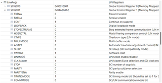
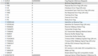
我发现 GPIO_22和 GPIO_23引脚分别用于 LIN_TX 和 LIN_Rx。 因此、我配置这些引脚并禁用内部回送模式。 为了进行传输、我只发送了两个字节的字符数据并进行了一些修改。 在示波器中、我观察到在 DMA 传输请求后、通过 GPIO_22引脚触发了单个脉冲、但未找到任何数据位或其他脉冲。  

我随函附上经修改的代码。 你的帮助将减轻我的负担。 请帮帮我。

//#############################################################################
 //
 // FILE:   lin_ex3_sci_dma.c
 //
 // TITLE:  LIN SCI MODE Internal Loopback with DMA
 //
 //! \addtogroup driver_example_list
 //! <h1> LIN SCI MODE Internal Loopback with DMA </h1>
 //!
 //! This example configures the LIN module in SCI mode for internal loopback
 //! with the use of the DMA. The LIN module performs as SCI with a set
 //! character and frame length in multi-buffer mode. When the transmit buffers
 //! in the LINTD0 and LINTD1 registers have enough space, the DMA will transfer
 //! data from global variable sData into those transmit registers. Once the
 //! received buffers in the LINRD0 and LINRD1 registers contain data,the DMA
 //! will transfer the data into the global variable rdata.
 //!
 //! When all data has been placed into rData, a check of the validity of the
 //! data will be performed in one of the DMA channels' ISRs.
 //!
 //! \b External \b Connections \n
 //!  - None
 //!
 //! \b Watch \b Variables \n
 //!  - \b sData - Data to send
 //!  - \b rData - Received data
 //!
 //
 //#############################################################################
 //
 //
 // $Copyright:
 // Copyright (C) 2022 Texas Instruments Incorporated - http://www.ti.com/
 //
 // Redistribution and use in source and binary forms, with or without
 // modification, are permitted provided that the following conditions
 // are met:
 //
 //   Redistributions of source code must retain the above copyright
 //   notice, this list of conditions and the following disclaimer.
 //
 //   Redistributions in binary form must reproduce the above copyright
 //   notice, this list of conditions and the following disclaimer in the
 //   documentation and/or other materials provided with the
 //   distribution.
 //
 //   Neither the name of Texas Instruments Incorporated nor the names of
 //   its contributors may be used to endorse or promote products derived
 //   from this software without specific prior written permission.
 //
 // THIS SOFTWARE IS PROVIDED BY THE COPYRIGHT HOLDERS AND CONTRIBUTORS
 // "AS IS" AND ANY EXPRESS OR IMPLIED WARRANTIES, INCLUDING, BUT NOT
 // LIMITED TO, THE IMPLIED WARRANTIES OF MERCHANTABILITY AND FITNESS FOR
 // A PARTICULAR PURPOSE ARE DISCLAIMED. IN NO EVENT SHALL THE COPYRIGHT
 // OWNER OR CONTRIBUTORS BE LIABLE FOR ANY DIRECT, INDIRECT, INCIDENTAL,
 // SPECIAL, EXEMPLARY, OR CONSEQUENTIAL DAMAGES (INCLUDING, BUT NOT
 // LIMITED TO, PROCUREMENT OF SUBSTITUTE GOODS OR SERVICES; LOSS OF USE,
 // DATA, OR PROFITS; OR BUSINESS INTERRUPTION) HOWEVER CAUSED AND ON ANY
 // THEORY OF LIABILITY, WHETHER IN CONTRACT, STRICT LIABILITY, OR TORT
 // (INCLUDING NEGLIGENCE OR OTHERWISE) ARISING IN ANY WAY OUT OF THE USE
 // OF THIS SOFTWARE, EVEN IF ADVISED OF THE POSSIBILITY OF SUCH DAMAGE.
 // $
 //#############################################################################

 //
 // Included Files
 //
 #include "driverlib.h"
 #include "device.h"

 //
 // Defines
 //
//Modified
 // #define BURST       4
// #define TRANSFER    32
// #define CHAR_LENGTH     8
// #define FRAME_LENGTH    8

#define BURST       1
#define TRANSFER    1
#define CHAR_LENGTH     8
#define FRAME_LENGTH    1

 //
 // Configure the Baud Rate to 115.207kHz
 //
 uint32_t PRESCALER=0x000001a;
 uint16_t DIVIDER=0x0002;

 //
 // Globals
 //
 //Modified
  uint16_t sData[2] = {'a', 'b'};
  uint16_t rData[2];
// unsigned char *sData;
// unsigned char *rData;

 //Place buffers in GSRAM
 #pragma DATA_SECTION(sData, "ramgs0");
 #pragma DATA_SECTION(rData, "ramgs0");

 volatile uint16_t done = 0;         // Flag to set when all data transfered

 //
 // Function Prototypes
 //
 void initDMA(void);
 void configureSCIMode(void);
 __interrupt void dmaCh5ISR(void);
 __interrupt void dmaCh6ISR(void);


 //
 // Main
 //
 void main(void)
 {
     //
     // Initialize device clock and peripherals
     //
     Device_init();

     //
     // Initialize GPIO
     //
     Device_initGPIO();

     // Pin config for LIN tx and LIN rx
     GPIO_setPinConfig(DEVICE_GPIO_CFG_LINTXA);
     GPIO_setPinConfig(DEVICE_GPIO_CFG_LINRXA);
     // GPIO_23 is used as LINTXA
     GPIO_setDirectionMode(23, GPIO_DIR_MODE_IN);
     GPIO_setPadConfig(23, GPIO_PIN_TYPE_PULLUP);
     GPIO_setQualificationMode(23, GPIO_QUAL_ASYNC);
     // GPIO_23 is used as LINRXA
     GPIO_setDirectionMode(22, GPIO_DIR_MODE_OUT);
     GPIO_setPadConfig(22, GPIO_PIN_TYPE_STD);
     GPIO_setQualificationMode(22, GPIO_QUAL_ASYNC);


     //
     // Initialize PIE and clear PIE registers. Disables CPU interrupts.
     //
     Interrupt_initModule();

     //
     // Initialize the PIE vector table with pointers to the shell Interrupt
     // Service Routines (ISR).
     //
     Interrupt_initVectorTable();
     EINT;
     ERTM;

     //
     // Interrupts that are used in this example are re-mapped to
     // ISR functions found within this file.
     // This registers the interrupt handler in PIE vector table.
     //
     Interrupt_register(INT_DMA_CH5, &dmaCh5ISR);
     Interrupt_register(INT_DMA_CH6, &dmaCh6ISR);

     //
     // Enable the DMA interrupt signals
     //
     Interrupt_enable(INT_DMA_CH5);
     Interrupt_enable(INT_DMA_CH6);

     //
     // Initialize the DMA
     //
     initDMA();

     //
     //Initialize the LIN Module
     //
     LIN_initModule(LINA_BASE);

     //
     // Configure the LIN module to operate in SCI mode
     //
     configureSCIMode();

     //
     // Initialize the data buffers
     //
//Modified
//     for(i = 0; i < 128; i++)
//     {
//        sData[i]= i;
//        rData[i]= 0;
//     }

     //
     // Wait for the SCI receiver to be idle
     //
     while(!LIN_isSCIReceiverIdle(LINA_BASE));

     //
     // Wait until space is available in the transmit buffer.
     //
     while(!LIN_isSCISpaceAvailable(LINA_BASE)){}
     //
     //Initiate transfer through a CPU write
     //
     LIN_sendData(LINA_BASE,(unsigned int*)0xFFFF);

     //
     // Start the DMA receive channel
     //
     DMA_startChannel(DMA_CH6_BASE);

     //
     //Start the DMA transmit channel
     //
     DMA_startChannel(DMA_CH5_BASE);

     //Write one data byte when Tx buffer is ready
     LIN_writeSCICharBlocking(LINA_BASE, sData[1]);
     //
     //Wait until the DMA transfer is complete
     //
//     while(!done);


     //
     //When the DMA transfer is complete the program will stop here
     //
     ESTOP0;

 }

 //
 // Function to configure LIN in SCI Mode
 //
 void
 configureSCIMode(void)
 {
     //
     // Enter LIN reset state to perform configurations
     //
     LIN_enterSoftwareReset(LINA_BASE);

     //
     // Switch LIN into SCI mode
     //
     LIN_enableSCIMode(LINA_BASE);

     //
     // Set the SCI communication mode to idle line
     //
     LIN_setSCICommMode(LINA_BASE, LIN_COMM_SCI_IDLELINE);

     //
     // Set SCI to transmit one stop bit
     //
     LIN_setSCIStopBits(LINA_BASE,LIN_SCI_STOP_ONE);

     //
     // Disable parity check
     //
     LIN_disableSCIParity(LINA_BASE);

//Modified
     //
     // Enable multi-buffer mode
     //
//     LIN_enableMultibufferMode(LINA_BASE);

     //
     // Module set to complete operations when halted by debugger
     //
     LIN_setDebugSuspendMode(LINA_BASE, LIN_DEBUG_COMPLETE);

     //
     // Set character length as 8-bits
     //
     LIN_setSCICharLength(LINA_BASE, CHAR_LENGTH);

     //
     // Set to 1 character in response field
     //
     LIN_setSCIFrameLength(LINA_BASE, FRAME_LENGTH);

     //
     // Set the Baud Rate
     //
     LIN_setBaudRatePrescaler(LINA_BASE, PRESCALER, DIVIDER);

//Modified
     //
     // Enable Internal Loopback mode
     //
//     LIN_enableIntLoopback(LINA_BASE);
//     LIN_disableIntLoopback(LINA_BASE);
     //
     //Enable the DMA for transmission
     //
     LIN_enableSCIInterrupt(LINA_BASE, LIN_SCI_INT_TX_DMA);

     //
     //Enable the DMA to receive
     //
     LIN_enableSCIInterrupt(LINA_BASE, LIN_SCI_INT_RX_DMA);


     // Exit LIN reset state
     //
     LIN_exitSoftwareReset(LINA_BASE);
 }

 //
 // DMA setup for both TX and RX channels.
 //
 void initDMA()
 {
     //
     // Initialize DMA
     //
     DMA_initController();

     //
     // Configure DMA Ch5 for TX. When there is enough space in the buffers found in
     // the LINTD0 and LINTD1 registers, data will be transferred from the sdata buffer
     // to the LIN's transmit registers. The destination address is configured to start
     // in the most significant part of the LINTD1 register (TD4/TD5 transmit buffers)and
     // move two address's down with every burst until it fills up the least significant
     // part of the LINTD0 register (TD2/ TD3 transmit buffers).After every transfer of
     // 4 bursts the destination address is brought back to the address of the TD4/TD5
     // buffers contained in the LINTD1 register.
     //

//Modified
//     DMA_configAddresses(DMA_CH5_BASE, (uint16_t *)(LINA_BASE + LIN_O_TD1+2), sData);
//     DMA_configBurst(DMA_CH5_BASE, BURST, 1, -2);
//     DMA_configTransfer(DMA_CH5_BASE, TRANSFER, 1, 6);
//     DMA_configMode(DMA_CH5_BASE, DMA_TRIGGER_LINATX, DMA_CFG_ONESHOT_DISABLE |
//                    DMA_CFG_CONTINUOUS_DISABLE | DMA_CFG_SIZE_16BIT);


     DMA_configAddresses(DMA_CH5_BASE, (uint16_t *)(LINA_BASE + LIN_O_SCITD), sData);
     DMA_configBurst(DMA_CH5_BASE, BURST, 0, 0);
     DMA_configTransfer(DMA_CH5_BASE, TRANSFER, 0, 0);
     DMA_configMode(DMA_CH5_BASE, DMA_TRIGGER_LINATX, DMA_CFG_ONESHOT_DISABLE |
                    DMA_CFG_CONTINUOUS_DISABLE | DMA_CFG_SIZE_16BIT);

     //
     // Configure DMA Ch5 interrupts
     //
     DMA_setInterruptMode(DMA_CH5_BASE, DMA_INT_AT_END);
     DMA_enableInterrupt(DMA_CH5_BASE);
     DMA_enableTrigger(DMA_CH5_BASE);

     //
     // Configure DMA Ch6 for RX. When the buffers found in the LINRD0 and LINRD1
     // registers are full, data will be transferred to the rdata buffer. The source
     // address is configured to start in the most significant part of the LINRD1
     // register (RD4/RD5 receive buffers) and move two address's down with every
     // burst until it transfers the least significant part of the LINTD0 register
     // (RD2/ RD3 receive buffers).After every transfer of 4 bursts the source
     // address is brought back to the address of the RD4/RD5 buffers contained in
     // the LINRD1 register.
     //

//Modified
//     DMA_configAddresses(DMA_CH6_BASE, rData,(uint16_t *)(LINA_BASE + LIN_O_RD1+2));
//     DMA_configBurst(DMA_CH6_BASE, BURST, -2, 1);
//     DMA_configTransfer(DMA_CH6_BASE, TRANSFER, 6, 1);
//     DMA_configMode(DMA_CH6_BASE, DMA_TRIGGER_LINARX, DMA_CFG_ONESHOT_DISABLE |
//                    DMA_CFG_CONTINUOUS_DISABLE | DMA_CFG_SIZE_16BIT);

     DMA_configAddresses(DMA_CH6_BASE, rData,(uint16_t *)(LIN_O_SCIRD));
     DMA_configBurst(DMA_CH6_BASE, BURST, 0, 0);
     DMA_configTransfer(DMA_CH6_BASE, TRANSFER, 0, 0);
     DMA_configMode(DMA_CH6_BASE, DMA_TRIGGER_LINARX, DMA_CFG_ONESHOT_DISABLE |
                    DMA_CFG_CONTINUOUS_DISABLE | DMA_CFG_SIZE_16BIT);

     //
     // Configure DMA Ch6 interrupts
     //
     DMA_setInterruptMode(DMA_CH6_BASE, DMA_INT_AT_END);
     DMA_enableInterrupt(DMA_CH6_BASE);
     DMA_enableTrigger(DMA_CH6_BASE);
 }

 //
 // DMA Channel 5 ISR
 //
 __interrupt void dmaCh5ISR(void)
 {
     DMA_stopChannel(DMA_CH5_BASE);
     Interrupt_clearACKGroup(INTERRUPT_ACK_GROUP7);
     return;
//     done = 1;
 }

 //
 // DMA Channel 6 ISR
 //
  __interrupt void dmaCh6ISR(void)
 {
     uint16_t i;
     DMA_stopChannel(DMA_CH6_BASE);
     Interrupt_clearACKGroup(INTERRUPT_ACK_GROUP7);

//Modified
 //    //
 //    //Check for data integrity
 //    //
 //    for(i=0; i<128; i++)
 //    {
 //        if(rData[i] !=i)
 //        {
 //           //Something went wrong, rdata doesn't contain expected data.
 //           ESTOP0;
 //        }
 //    }

//     done = 1;
     return;
 }

  • 请注意,本文内容源自机器翻译,可能存在语法或其它翻译错误,仅供参考。如需获取准确内容,请参阅链接中的英语原文或自行翻译。

    您好、Masud、

    感谢您的问题(非常感谢您对代码块中的代码进行格式化!)。


    我认为问题的部分原因是 writeSCICharClocking 与之前的"LIN_sendData"调用冲突:

    (左侧是原始示例、右侧是提供的代码)

    当您在其中中间执行另一个 LIN_writeSciCharBlocking 时、LIN_sendData 可能仍在发送数据。 由于缓冲区设置为仅1个字节、因此可能存在冲突。

    不过、为了确定问题、能否提供 LIN 寄存器集中所有错误寄存器的值?

    此致、

    Vince

  • 请注意,本文内容源自机器翻译,可能存在语法或其它翻译错误,仅供参考。如需获取准确内容,请参阅链接中的英语原文或自行翻译。

    尊敬的 Vince:

    非常感谢您的即时回复。

    如果我使用  LIN_writeSciCharBlocking 以连续方式发送多个字节、那么也不会产生任何结果。  

    我要在 Lina 中附加全局控制寄存器和标志寄存器的值。 请仔细阅读。

    再次感谢您的帮助。

    此致、

    Masud

  • 请注意,本文内容源自机器翻译,可能存在语法或其它翻译错误,仅供参考。如需获取准确内容,请参阅链接中的英语原文或自行翻译。

    您好、Masud、


    感谢您提供寄存器、这对您有很大帮助。

    因此、看起来会发生两种情况、这两种情况都是潜在的调试路径:

    TXENA 和 RXENA 位未置位(因此不会发生数据发送或接收)。

    对于这个、让我们在初始化代码中的以下两个函数在数据传输到移位寄存器之前的 somwhere (在 writeChar 函数之前):

    LIN_enableDataTransmitter

    LIN_enableDataReceiver


    这将启用 TXENA 和 RXENA 位、见下图:


    2、SCIFLR.PE 位置位、因此在屏幕截图之前的某个点、出现了奇偶校验错误。 让我们首先修复#1、然后我们可以看到有关此问题的信息。


    此致、

    Vince

  • 请注意,本文内容源自机器翻译,可能存在语法或其它翻译错误,仅供参考。如需获取准确内容,请参阅链接中的英语原文或自行翻译。

    尊敬的 Vince:

    感谢您提供重要信息。

    您的宝贵答复帮助我通过 DMA 将数据字节从存储器传输到终端。 您应该得到非常感谢。

    现在、只有我在接收数据字节时遇到问题。

    根据您的建议、我将 LIN_enableDataTransmitter、LIN_enableDataReceiver 函数置于 configureSCIMode 中。 我想理解、如果我们在 DMA 中使用 LIN_writeSciCharArray 函数、这并不意味着 CPU 传输数据而不是 DMA。 如果是、那么我不应该包含 writeChar 或 readChar 函数、因为根据我的理解、当发生 DMA 请求时、内存和缓冲寄存器之间的传输会自动更新。

    为了理解这个概念、我修改了代码的小位、并随函附上、请仔细阅读。  

    我看到 SCIRD 寄存器根据从终端接收到的字符进行了更新、但在 RDATA 变量中没有更新。 每次 SCIRD 寄存器接收到数据字节时、它都会触发 DMA 请求、那么为什么变量不会更新?

    代码如下:

       //#############################################################################
        //
        // FILE:   lin_ex3_sci_dma.c
        //
        // TITLE:  LIN SCI MODE Internal Loopback with DMA
        //
        //! \addtogroup driver_example_list
        //! <h1> LIN SCI MODE Internal Loopback with DMA </h1>
        //!
        //! This example configures the LIN module in SCI mode for internal loopback
        //! with the use of the DMA. The LIN module performs as SCI with a set
        //! character and frame length in multi-buffer mode. When the transmit buffers
        //! in the LINTD0 and LINTD1 registers have enough space, the DMA will transfer
        //! data from global variable sData into those transmit registers. Once the
        //! received buffers in the LINRD0 and LINRD1 registers contain data,the DMA
        //! will transfer the data into the global variable rdata.
        //!
        //! When all data has been placed into rData, a check of the validity of the
        //! data will be performed in one of the DMA channels' ISRs.
        //!
        //! \b External \b Connections \n
        //!  - None
        //!
        //! \b Watch \b Variables \n
        //!  - \b sData - Data to send
        //!  - \b rData - Received data
        //!
        //
        //#############################################################################
        //
        //
        // $Copyright:
        // Copyright (C) 2022 Texas Instruments Incorporated - http://www.ti.com/
        //
        // Redistribution and use in source and binary forms, with or without
        // modification, are permitted provided that the following conditions
        // are met:
        //
        //   Redistributions of source code must retain the above copyright
        //   notice, this list of conditions and the following disclaimer.
        //
        //   Redistributions in binary form must reproduce the above copyright
        //   notice, this list of conditions and the following disclaimer in the
        //   documentation and/or other materials provided with the
        //   distribution.
        //
        //   Neither the name of Texas Instruments Incorporated nor the names of
        //   its contributors may be used to endorse or promote products derived
        //   from this software without specific prior written permission.
        //
        // THIS SOFTWARE IS PROVIDED BY THE COPYRIGHT HOLDERS AND CONTRIBUTORS
        // "AS IS" AND ANY EXPRESS OR IMPLIED WARRANTIES, INCLUDING, BUT NOT
        // LIMITED TO, THE IMPLIED WARRANTIES OF MERCHANTABILITY AND FITNESS FOR
        // A PARTICULAR PURPOSE ARE DISCLAIMED. IN NO EVENT SHALL THE COPYRIGHT
        // OWNER OR CONTRIBUTORS BE LIABLE FOR ANY DIRECT, INDIRECT, INCIDENTAL,
        // SPECIAL, EXEMPLARY, OR CONSEQUENTIAL DAMAGES (INCLUDING, BUT NOT
        // LIMITED TO, PROCUREMENT OF SUBSTITUTE GOODS OR SERVICES; LOSS OF USE,
        // DATA, OR PROFITS; OR BUSINESS INTERRUPTION) HOWEVER CAUSED AND ON ANY
        // THEORY OF LIABILITY, WHETHER IN CONTRACT, STRICT LIABILITY, OR TORT
        // (INCLUDING NEGLIGENCE OR OTHERWISE) ARISING IN ANY WAY OUT OF THE USE
        // OF THIS SOFTWARE, EVEN IF ADVISED OF THE POSSIBILITY OF SUCH DAMAGE.
        // $
        //#############################################################################
    
        //
        // Included Files
        //
        #include "driverlib.h"
        #include "device.h"
    
        //
        // Defines
        //
       //Modified
        // #define BURST       4
       // #define TRANSFER    32
       // #define CHAR_LENGTH     8
       // #define FRAME_LENGTH    8
    
       #define BURST       1
       #define TRANSFER    6
       #define CHAR_LENGTH     8
       #define FRAME_LENGTH    1
    
        //
        // Configure the Baud Rate to 115.207kHz
        //
        uint32_t PRESCALER=0x000001a;
        uint16_t DIVIDER=0x0002;
    
        //
        // Globals
        //
        //Modified
         uint16_t sData[6] = {'a', 'b', 'c','d','e', 'f'};
         uint16_t rData[4];
       // unsigned char *sData;
       // unsigned char *rData;
    
        //Place buffers in GSRAM
        #pragma DATA_SECTION(sData, "ramgs0");
        #pragma DATA_SECTION(rData, "ramgs0");
    
    //    volatile uint16_t done = 0;         // Flag to set when all data transfered
    
        //
        // Function Prototypes
        //
        void initDMA(void);
        void configureSCIMode(void);
        __interrupt void dmaCh5ISR(void);
        __interrupt void dmaCh6ISR(void);
    
    
        //
        // Main
        //
        void main(void)
        {
            //
            // Initialize device clock and peripherals
            //
            Device_init();
    
            //
            // Initialize GPIO
            //
            Device_initGPIO();
    
            // Pin config for LIN tx and LIN rx
            GPIO_setPinConfig(DEVICE_GPIO_CFG_LINTXA);
            GPIO_setPinConfig(DEVICE_GPIO_CFG_LINRXA);
            // GPIO_23 is used as LINTXA
            GPIO_setDirectionMode(23, GPIO_DIR_MODE_IN);
            GPIO_setPadConfig(23, GPIO_PIN_TYPE_PULLUP);
            GPIO_setQualificationMode(23, GPIO_QUAL_ASYNC);
            // GPIO_23 is used as LINRXA
            GPIO_setDirectionMode(22, GPIO_DIR_MODE_OUT);
            GPIO_setPadConfig(22, GPIO_PIN_TYPE_STD);
            GPIO_setQualificationMode(22, GPIO_QUAL_ASYNC);
    
    
            //
            // Initialize PIE and clear PIE registers. Disables CPU interrupts.
            //
            Interrupt_initModule();
    
            //
            // Initialize the PIE vector table with pointers to the shell Interrupt
            // Service Routines (ISR).
            //
            Interrupt_initVectorTable();
            EINT;
            ERTM;
    
            //
            // Interrupts that are used in this example are re-mapped to
            // ISR functions found within this file.
            // This registers the interrupt handler in PIE vector table.
            //
            Interrupt_register(INT_DMA_CH5, &dmaCh5ISR);
            Interrupt_register(INT_DMA_CH6, &dmaCh6ISR);
    
            //
            // Enable the DMA interrupt signals
            //
            Interrupt_enable(INT_DMA_CH5);
            Interrupt_enable(INT_DMA_CH6);
    
            //
            // Initialize the DMA
            //
            initDMA();
    
            //
            //Initialize the LIN Module
            //
            LIN_initModule(LINA_BASE);
    
            //
            // Configure the LIN module to operate in SCI mode
            //
            configureSCIMode();
    
            //
            // Initialize the data buffers
            //
       //Modified
       //     for(i = 0; i < 128; i++)
       //     {
       //        sData[i]= i;
       //        rData[i]= 0;
       //     }
    
            //
            // Wait for the SCI receiver to be idle
            //
            while(!LIN_isSCIReceiverIdle(LINA_BASE));
    
            //
            // Wait until space is available in the transmit buffer.
            //
            while(!LIN_isSCISpaceAvailable(LINA_BASE)){}
            //
            //Initiate transfer through a CPU write
            //
            LIN_sendData(LINA_BASE,(unsigned int*)0xFFFF);
    
            //
            // Start the DMA receive channel
            //
            DMA_startChannel(DMA_CH6_BASE);
    
            //
            //Start the DMA transmit channel
            //
            DMA_startChannel(DMA_CH5_BASE);
    
            //Write one data byte when Tx buffer is ready
    //        LIN_writeSCICharBlocking(LINA_BASE, sData[1]);
            //
            //Wait until the DMA transfer is complete
            //
    //        while(!done);
    //        for(;;);
    
            //
            //When the DMA transfer is complete the program will stop here
            //
    //        ESTOP0;
    
        }
    
        //
        // Function to configure LIN in SCI Mode
        //
        void
        configureSCIMode(void)
        {
            //
            // Enter LIN reset state to perform configurations
            //
            LIN_enterSoftwareReset(LINA_BASE);
    
            //
            // Switch LIN into SCI mode
            //
            LIN_enableSCIMode(LINA_BASE);
    
            //
            // Set the SCI communication mode to idle line
            //
            LIN_setSCICommMode(LINA_BASE, LIN_COMM_SCI_IDLELINE);
    
            //
            // Set SCI to transmit one stop bit
            //
            LIN_setSCIStopBits(LINA_BASE,LIN_SCI_STOP_ONE);
    
            //
            // Disable parity check
            //
            LIN_disableSCIParity(LINA_BASE);
    
       //Modified
            //
            // Enable multi-buffer mode
            //
       //     LIN_enableMultibufferMode(LINA_BASE);
            LIN_disableMultibufferMode(LINA_BASE);
    
            //
            // Module set to complete operations when halted by debugger
            //
            LIN_setDebugSuspendMode(LINA_BASE, LIN_DEBUG_COMPLETE);
    
            //
            // Set character length as 8-bits
            //
            LIN_setSCICharLength(LINA_BASE, CHAR_LENGTH);
    
            //
            // Set to 1 character in response field
            //
            LIN_setSCIFrameLength(LINA_BASE, FRAME_LENGTH);
    
            //
            // Set the Baud Rate
            //
            LIN_setBaudRatePrescaler(LINA_BASE, PRESCALER, DIVIDER);
    
       //Modified
            //
            // Enable Internal Loopback mode
            //
       //     LIN_enableIntLoopback(LINA_BASE);
       //     LIN_disableIntLoopback(LINA_BASE);
    
            LIN_enableDataTransmitter(LINA_BASE);
            LIN_enableDataReceiver(LINA_BASE);
            //
            //Enable the DMA for transmission
            //
            LIN_enableSCIInterrupt(LINA_BASE, LIN_SCI_INT_TX_DMA);
    
            //
            //Enable the DMA to receive
            //
            LIN_enableSCIInterrupt(LINA_BASE, LIN_SCI_INT_RX_DMA);
    
    
            // Exit LIN reset state
            //
            LIN_exitSoftwareReset(LINA_BASE);
        }
    
        //
        // DMA setup for both TX and RX channels.
        //
        void initDMA()
        {
            //
            // Initialize DMA
            //
            DMA_initController();
    
            //
            // Configure DMA Ch5 for TX. When there is enough space in the buffers found in
            // the LINTD0 and LINTD1 registers, data will be transferred from the sdata buffer
            // to the LIN's transmit registers. The destination address is configured to start
            // in the most significant part of the LINTD1 register (TD4/TD5 transmit buffers)and
            // move two address's down with every burst until it fills up the least significant
            // part of the LINTD0 register (TD2/ TD3 transmit buffers).After every transfer of
            // 4 bursts the destination address is brought back to the address of the TD4/TD5
            // buffers contained in the LINTD1 register.
            //
    
       //Modified
    //        DMA_configAddresses(DMA_CH5_BASE, (uint16_t *)(LINA_BASE + LIN_O_TD1+2), sData);
    //        DMA_configBurst(DMA_CH5_BASE, BURST, 1, -2);
    //        DMA_configTransfer(DMA_CH5_BASE, TRANSFER, 1, 6);
    //        DMA_configMode(DMA_CH5_BASE, DMA_TRIGGER_LINATX, DMA_CFG_ONESHOT_DISABLE |
    //                       DMA_CFG_CONTINUOUS_DISABLE | DMA_CFG_SIZE_16BIT);
    
    //
            DMA_configAddresses(DMA_CH5_BASE, (uint16_t *)(LINA_BASE + LIN_O_SCITD), sData);
            DMA_configBurst(DMA_CH5_BASE, BURST, 4, 0);
            DMA_configTransfer(DMA_CH5_BASE, TRANSFER, 1, 0);
            DMA_configMode(DMA_CH5_BASE, DMA_TRIGGER_LINATX, DMA_CFG_ONESHOT_DISABLE |
                           DMA_CFG_CONTINUOUS_DISABLE | DMA_CFG_SIZE_16BIT);
    
            //
            // Configure DMA Ch5 interrupts
            //
            DMA_setInterruptMode(DMA_CH5_BASE, DMA_INT_AT_END);
            DMA_enableInterrupt(DMA_CH5_BASE);
            DMA_enableTrigger(DMA_CH5_BASE);
    
            //
            // Configure DMA Ch6 for RX. When the buffers found in the LINRD0 and LINRD1
            // registers are full, data will be transferred to the rdata buffer. The source
            // address is configured to start in the most significant part of the LINRD1
            // register (RD4/RD5 receive buffers) and move two address's down with every
            // burst until it transfers the least significant part of the LINTD0 register
            // (RD2/ RD3 receive buffers).After every transfer of 4 bursts the source
            // address is brought back to the address of the RD4/RD5 buffers contained in
            // the LINRD1 register.
            //
    
       //Modified
       //     DMA_configAddresses(DMA_CH6_BASE, rData,(uint16_t *)(LINA_BASE + LIN_O_RD1+2));
       //     DMA_configBurst(DMA_CH6_BASE, BURST, -2, 1);
       //     DMA_configTransfer(DMA_CH6_BASE, TRANSFER, 6, 1);
       //     DMA_configMode(DMA_CH6_BASE, DMA_TRIGGER_LINARX, DMA_CFG_ONESHOT_DISABLE |
       //                    DMA_CFG_CONTINUOUS_DISABLE | DMA_CFG_SIZE_16BIT);
    
            DMA_configAddresses(DMA_CH6_BASE, rData,(uint16_t *)(LIN_O_SCIRD));
            DMA_configBurst(DMA_CH6_BASE, BURST, 0, 4);
            DMA_configTransfer(DMA_CH6_BASE, TRANSFER, 0, 1);
            DMA_configMode(DMA_CH6_BASE, DMA_TRIGGER_LINARX, DMA_CFG_ONESHOT_DISABLE |
                           DMA_CFG_CONTINUOUS_DISABLE | DMA_CFG_SIZE_16BIT);
    
            //
            // Configure DMA Ch6 interrupts
            //
            DMA_setInterruptMode(DMA_CH6_BASE, DMA_INT_AT_END);
            DMA_enableInterrupt(DMA_CH6_BASE);
            DMA_enableTrigger(DMA_CH6_BASE);
        }
    
        //
        // DMA Channel 5 ISR
        //
        __interrupt void dmaCh5ISR(void)
        {
            DMA_stopChannel(DMA_CH5_BASE);
            Interrupt_clearACKGroup(INTERRUPT_ACK_GROUP7);
            return;
    //        done = 1;
        }
    
        //
        // DMA Channel 6 ISR
        //
         __interrupt void dmaCh6ISR(void)
        {
            uint16_t i;
            DMA_stopChannel(DMA_CH6_BASE);
            Interrupt_clearACKGroup(INTERRUPT_ACK_GROUP7);
    
       //Modified
        //    //
        //    //Check for data integrity
        //    //
        //    for(i=0; i<128; i++)
        //    {
        //        if(rData[i] !=i)
        //        {
        //           //Something went wrong, rdata doesn't contain expected data.
        //           ESTOP0;
        //        }
        //    }
    
    //        done = 1;
            return;
        }

    谢谢、此致、

    Masud

  • 请注意,本文内容源自机器翻译,可能存在语法或其它翻译错误,仅供参考。如需获取准确内容,请参阅链接中的英语原文或自行翻译。

    您好、Masud、

    很高兴您能够使发送器正常工作。 回答有关 DMA 的问题:请参阅具有"LIN_O_SCIRD"的行。 这缺少"Lina_base"偏移、因此指向内存中的错误位置。

     '

    请参阅上述左侧=原始代码、右侧=提供的代码之间的比较。

    具体来说,此行不正确,需要有“Lina_base”,如 TX:

    DMA_configAddresses(DMA_CH6_BASE, rData,(uint16_t *)(LIN_O_SCIRD));

    此致、

    Vince

  • 请注意,本文内容源自机器翻译,可能存在语法或其它翻译错误,仅供参考。如需获取准确内容,请参阅链接中的英语原文或自行翻译。

    尊敬的 Vince:

    我已经添加了带有 LIN_O_SCIRD 的 Lina_base、那么结果也不会在 RDATA 变量中更新。 数据字节由 SCIRD 缓冲寄存器接收并反映在寄存器部分。 我还尝试使用单个 RDATA 变量而不是数组、并将地址传递给 DMA_CONFIGAddresses (DMA_CH6_BASE、&RDATA、(uint16_t *)(Lina_base_LIN_O_SCIRD);我认为它非常接近、但犯了一些我无法确定的错误。

    谢谢、此致、

    Masud

  • 请注意,本文内容源自机器翻译,可能存在语法或其它翻译错误,仅供参考。如需获取准确内容,请参阅链接中的英语原文或自行翻译。

    您好、Masud、

    您能否显示具有 Lina_base 和 LIN_O_SCIRD 的更新行? 我想回顾一下该部分代码。


    此致、

    Vince

  • 请注意,本文内容源自机器翻译,可能存在语法或其它翻译错误,仅供参考。如需获取准确内容,请参阅链接中的英语原文或自行翻译。

    尊敬的 Vince:

    很抱歉、我的回答很晚、遇到了健康问题。

    以下是更新后的代码:

    //#############################################################################
        //
        // FILE:   lin_ex3_sci_dma.c
        //
        // TITLE:  LIN SCI MODE Internal Loopback with DMA
        //
        //! \addtogroup driver_example_list
        //! <h1> LIN SCI MODE Internal Loopback with DMA </h1>
        //!
        //! This example configures the LIN module in SCI mode for internal loopback
        //! with the use of the DMA. The LIN module performs as SCI with a set
        //! character and frame length in multi-buffer mode. When the transmit buffers
        //! in the LINTD0 and LINTD1 registers have enough space, the DMA will transfer
        //! data from global variable sData into those transmit registers. Once the
        //! received buffers in the LINRD0 and LINRD1 registers contain data,the DMA
        //! will transfer the data into the global variable rdata.
        //!
        //! When all data has been placed into rData, a check of the validity of the
        //! data will be performed in one of the DMA channels' ISRs.
        //!
        //! \b External \b Connections \n
        //!  - None
        //!
        //! \b Watch \b Variables \n
        //!  - \b sData - Data to send
        //!  - \b rData - Received data
        //!
        //
        //#############################################################################
        //
        //
        // $Copyright:
        // Copyright (C) 2022 Texas Instruments Incorporated - http://www.ti.com/
        //
        // Redistribution and use in source and binary forms, with or without
        // modification, are permitted provided that the following conditions
        // are met:
        //
        //   Redistributions of source code must retain the above copyright
        //   notice, this list of conditions and the following disclaimer.
        //
        //   Redistributions in binary form must reproduce the above copyright
        //   notice, this list of conditions and the following disclaimer in the
        //   documentation and/or other materials provided with the
        //   distribution.
        //
        //   Neither the name of Texas Instruments Incorporated nor the names of
        //   its contributors may be used to endorse or promote products derived
        //   from this software without specific prior written permission.
        //
        // THIS SOFTWARE IS PROVIDED BY THE COPYRIGHT HOLDERS AND CONTRIBUTORS
        // "AS IS" AND ANY EXPRESS OR IMPLIED WARRANTIES, INCLUDING, BUT NOT
        // LIMITED TO, THE IMPLIED WARRANTIES OF MERCHANTABILITY AND FITNESS FOR
        // A PARTICULAR PURPOSE ARE DISCLAIMED. IN NO EVENT SHALL THE COPYRIGHT
        // OWNER OR CONTRIBUTORS BE LIABLE FOR ANY DIRECT, INDIRECT, INCIDENTAL,
        // SPECIAL, EXEMPLARY, OR CONSEQUENTIAL DAMAGES (INCLUDING, BUT NOT
        // LIMITED TO, PROCUREMENT OF SUBSTITUTE GOODS OR SERVICES; LOSS OF USE,
        // DATA, OR PROFITS; OR BUSINESS INTERRUPTION) HOWEVER CAUSED AND ON ANY
        // THEORY OF LIABILITY, WHETHER IN CONTRACT, STRICT LIABILITY, OR TORT
        // (INCLUDING NEGLIGENCE OR OTHERWISE) ARISING IN ANY WAY OUT OF THE USE
        // OF THIS SOFTWARE, EVEN IF ADVISED OF THE POSSIBILITY OF SUCH DAMAGE.
        // $
        //#############################################################################
    
        //
        // Included Files
        //
        #include "driverlib.h"
        #include "device.h"
    
        //
        // Defines
        //
       //Modified
        // #define BURST       4
       // #define TRANSFER    32
       // #define CHAR_LENGTH     8
       // #define FRAME_LENGTH    8
    
       #define BURST       1
       #define TRANSFER    6
       #define CHAR_LENGTH     8
       #define FRAME_LENGTH    1
    
        //
        // Configure the Baud Rate to 115.207kHz
        //
        uint32_t PRESCALER=0x000001a;
        uint16_t DIVIDER=0x0002;
    
        //
        // Globals
        //
        //Modified
         uint16_t sData[6] = {'a', 'b', 'c','d','e', 'f'};
         uint16_t rData[4];
       // unsigned char *sData;
    //     uint16_t *rData;
    //     uint16_t rData;
         uint16_t i;
        //Place buffers in GSRAM
        #pragma DATA_SECTION(sData, "ramgs0");
        #pragma DATA_SECTION(rData, "ramgs0");
    
    //    volatile uint16_t done = 0;         // Flag to set when all data transfered
    
        //
        // Function Prototypes
        //
        void initDMA(void);
        void configureSCIMode(void);
        __interrupt void dmaCh5ISR(void);
        __interrupt void dmaCh6ISR(void);
    
    
        //
        // Main
        //
        void main(void)
        {
            //
            // Initialize device clock and peripherals
            //
            Device_init();
    
            //
            // Initialize GPIO
            //
            Device_initGPIO();
    
            // Pin config for LIN tx and LIN rx
            GPIO_setPinConfig(DEVICE_GPIO_CFG_LINTXA);
            GPIO_setPinConfig(DEVICE_GPIO_CFG_LINRXA);
            // GPIO_23 is used as LINTXA
            GPIO_setDirectionMode(29, GPIO_DIR_MODE_IN);
            GPIO_setPadConfig(29, GPIO_PIN_TYPE_PULLUP);
            GPIO_setQualificationMode(29, GPIO_QUAL_ASYNC);
            // GPIO_23 is used as LINRXA
            GPIO_setDirectionMode(28, GPIO_DIR_MODE_OUT);
            GPIO_setPadConfig(28, GPIO_PIN_TYPE_STD);
            GPIO_setQualificationMode(28, GPIO_QUAL_ASYNC);
    
    
            //
            // Initialize PIE and clear PIE registers. Disables CPU interrupts.
            //
            Interrupt_initModule();
    
            //
            // Initialize the PIE vector table with pointers to the shell Interrupt
            // Service Routines (ISR).
            //
            Interrupt_initVectorTable();
            EINT;
            ERTM;
    
            //
            // Interrupts that are used in this example are re-mapped to
            // ISR functions found within this file.
            // This registers the interrupt handler in PIE vector table.
            //
            Interrupt_register(INT_DMA_CH5, &dmaCh5ISR);
            Interrupt_register(INT_DMA_CH6, &dmaCh6ISR);
    
            //
            // Enable the DMA interrupt signals
            //
            Interrupt_enable(INT_DMA_CH5);
            Interrupt_enable(INT_DMA_CH6);
    
            //
            // Initialize the DMA
            //
            initDMA();
    
            //
            //Initialize the LIN Module
            //
            LIN_initModule(LINA_BASE);
    
            //
            // Configure the LIN module to operate in SCI mode
            //
            configureSCIMode();
    
            //
            // Initialize the data buffers
            //
       //Modified
       //     for(i = 0; i < 128; i++)
       //     {
       //        sData[i]= i;
       //        rData[i]= 0;
       //     }
    
            //
            // Wait for the SCI receiver to be idle
            //
            while(!LIN_isSCIReceiverIdle(LINA_BASE));
    
            //
            // Wait until space is available in the transmit buffer.
            //
            while(!LIN_isSCISpaceAvailable(LINA_BASE)){}
            //
            //Initiate transfer through a CPU write
            //
            LIN_sendData(LINA_BASE,(unsigned int*)0xFFFF);
    
            //
            // Start the DMA receive channel
            //
            DMA_startChannel(DMA_CH6_BASE);
    
            //
            //Start the DMA transmit channel
            //
    //        DMA_startChannel(DMA_CH5_BASE);
    
    
            DMA_startChannel(DMA_CH5_BASE);
    
            //Write one data byte when Tx buffer is ready
    //        LIN_writeSCICharBlocking(LINA_BASE, sData[1]);
            //
            //Wait until the DMA transfer is complete
            //
    //        while(!done);
    //        for(;;);
    
            //
            //When the DMA transfer is complete the program will stop here
            //
    //        ESTOP0;
    
        }
    
        //
        // Function to configure LIN in SCI Mode
        //
        void
        configureSCIMode(void)
        {
            //
            // Enter LIN reset state to perform configurations
            //
            LIN_enterSoftwareReset(LINA_BASE);
    
            //
            // Switch LIN into SCI mode
            //
            LIN_enableSCIMode(LINA_BASE);
    
            //
            // Set the SCI communication mode to idle line
            //
            LIN_setSCICommMode(LINA_BASE, LIN_COMM_SCI_IDLELINE);
    
            //
            // Set SCI to transmit one stop bit
            //
            LIN_setSCIStopBits(LINA_BASE,LIN_SCI_STOP_ONE);
    
            //
            // Disable parity check
            //
            LIN_disableSCIParity(LINA_BASE);
    
       //Modified
            //
            // Enable multi-buffer mode
            //
       //     LIN_enableMultibufferMode(LINA_BASE);
            LIN_disableMultibufferMode(LINA_BASE);
    
            //
            // Module set to complete operations when halted by debugger
            //
            LIN_setDebugSuspendMode(LINA_BASE, LIN_DEBUG_COMPLETE);
    
            //
            // Set character length as 8-bits
            //
            LIN_setSCICharLength(LINA_BASE, CHAR_LENGTH);
    
            //
            // Set to 1 character in response field
            //
            LIN_setSCIFrameLength(LINA_BASE, FRAME_LENGTH);
    
            //
            // Set the Baud Rate
            //
            LIN_setBaudRatePrescaler(LINA_BASE, PRESCALER, DIVIDER);
    
       //Modified
            //
            // Enable Internal Loopback mode
            //
       //     LIN_enableIntLoopback(LINA_BASE);
       //     LIN_disableIntLoopback(LINA_BASE);
    
            LIN_enableDataTransmitter(LINA_BASE);
            LIN_enableDataReceiver(LINA_BASE);
            //
            //Enable the DMA for transmission
            //
            LIN_enableSCIInterrupt(LINA_BASE, LIN_SCI_INT_TX_DMA);
    
            //
            //Enable the DMA to receive
            //
            LIN_enableSCIInterrupt(LINA_BASE, LIN_SCI_INT_RX_DMA);
    
    
            // Exit LIN reset state
            //
            LIN_exitSoftwareReset(LINA_BASE);
        }
    
        //
        // DMA setup for both TX and RX channels.
        //
        void initDMA()
        {
            //
            // Initialize DMA
            //
            DMA_initController();
    
            //
            // Configure DMA Ch5 for TX. When there is enough space in the buffers found in
            // the LINTD0 and LINTD1 registers, data will be transferred from the sdata buffer
            // to the LIN's transmit registers. The destination address is configured to start
            // in the most significant part of the LINTD1 register (TD4/TD5 transmit buffers)and
            // move two address's down with every burst until it fills up the least significant
            // part of the LINTD0 register (TD2/ TD3 transmit buffers).After every transfer of
            // 4 bursts the destination address is brought back to the address of the TD4/TD5
            // buffers contained in the LINTD1 register.
            //
    
       //Modified
    //        DMA_configAddresses(DMA_CH5_BASE, (uint16_t *)(LINA_BASE + LIN_O_TD1+2), sData);
    //        DMA_configBurst(DMA_CH5_BASE, BURST, 1, -2);
    //        DMA_configTransfer(DMA_CH5_BASE, TRANSFER, 1, 6);
    //        DMA_configMode(DMA_CH5_BASE, DMA_TRIGGER_LINATX, DMA_CFG_ONESHOT_DISABLE |
    //                       DMA_CFG_CONTINUOUS_DISABLE | DMA_CFG_SIZE_16BIT);
    
    //
            DMA_configAddresses(DMA_CH5_BASE, (uint16_t *)(LINA_BASE + LIN_O_SCITD), sData);
            DMA_configBurst(DMA_CH5_BASE, BURST, 4, 0);
            DMA_configTransfer(DMA_CH5_BASE, TRANSFER, 1, 0);
            DMA_configMode(DMA_CH5_BASE, DMA_TRIGGER_LINATX, DMA_CFG_ONESHOT_DISABLE |
                           DMA_CFG_CONTINUOUS_DISABLE | DMA_CFG_SIZE_16BIT);
    
            //
            // Configure DMA Ch5 interrupts
            //
            DMA_setInterruptMode(DMA_CH5_BASE, DMA_INT_AT_END);
            DMA_enableInterrupt(DMA_CH5_BASE);
            DMA_enableTrigger(DMA_CH5_BASE);
    
            //
            // Configure DMA Ch6 for RX. When the buffers found in the LINRD0 and LINRD1
            // registers are full, data will be transferred to the rdata buffer. The source
            // address is configured to start in the most significant part of the LINRD1
            // register (RD4/RD5 receive buffers) and move two address's down with every
            // burst until it transfers the least significant part of the LINTD0 register
            // (RD2/ RD3 receive buffers).After every transfer of 4 bursts the source
            // address is brought back to the address of the RD4/RD5 buffers contained in
            // the LINRD1 register.
            //
    
       //Modified
       //     DMA_configAddresses(DMA_CH6_BASE, rData,(uint16_t *)(LINA_BASE + LIN_O_RD1+2));
       //     DMA_configBurst(DMA_CH6_BASE, BURST, -2, 1);
       //     DMA_configTransfer(DMA_CH6_BASE, TRANSFER, 6, 1);
       //     DMA_configMode(DMA_CH6_BASE, DMA_TRIGGER_LINARX, DMA_CFG_ONESHOT_DISABLE |
       //                    DMA_CFG_CONTINUOUS_DISABLE | DMA_CFG_SIZE_16BIT);
    
            DMA_configAddresses(DMA_CH6_BASE, rData,(uint16_t *)(LINA_BASE + LIN_O_SCIRD));
            DMA_configBurst(DMA_CH6_BASE, BURST, 0, 4);
            DMA_configTransfer(DMA_CH6_BASE, TRANSFER, 0, 1);
            DMA_configMode(DMA_CH6_BASE, DMA_TRIGGER_LINARX, DMA_CFG_ONESHOT_DISABLE |
                           DMA_CFG_CONTINUOUS_DISABLE | DMA_CFG_SIZE_16BIT);
    
            //
            // Configure DMA Ch6 interrupts
            //
            DMA_setInterruptMode(DMA_CH6_BASE, DMA_INT_AT_END);
            DMA_enableInterrupt(DMA_CH6_BASE);
            DMA_enableTrigger(DMA_CH6_BASE);
        }
    
        //
        // DMA Channel 5 ISR
        //
        __interrupt void dmaCh5ISR(void)
        {
            DMA_stopChannel(DMA_CH5_BASE);
            Interrupt_clearACKGroup(INTERRUPT_ACK_GROUP7);
            return;
    //        done = 1;
        }
    
        //
        // DMA Channel 6 ISR
        //
         __interrupt void dmaCh6ISR(void)
        {
            uint16_t i;
            DMA_stopChannel(DMA_CH6_BASE);
            Interrupt_clearACKGroup(INTERRUPT_ACK_GROUP7);
    
       //Modified
        //    //
        //    //Check for data integrity
        //    //
        //    for(i=0; i<128; i++)
        //    {
        //        if(rData[i] !=i)
        //        {
        //           //Something went wrong, rdata doesn't contain expected data.
        //           ESTOP0;
        //        }
        //    }
    
    //        done = 1;
            return;
        }
    

    我检查了代码、但没有发现任何问题、如果 SCIRD 地址不正确、那么 SCIRD 缓冲寄存器如何接收数据?

    但在 RDATA 中不接收任何内容。

    感谢您的考虑。

    此致、

  • 请注意,本文内容源自机器翻译,可能存在语法或其它翻译错误,仅供参考。如需获取准确内容,请参阅链接中的英语原文或自行翻译。

    您好、Masud、

    您的主代码在末尾似乎没有 while 循环来保持程序运行。 是否有可能在 RX 能够接收之前程序刚刚结束?

    无论采用哪种方法、我都建议您在主循环的末尾放置一个"while (1);"。

    此致、

    Vince