This thread has been locked.
If you have a related question, please click the "Ask a related question" button in the top right corner. The newly created question will be automatically linked to this question.
尊敬的 TI 成员:
我将为 PID 附加一个仿真代码。 我需要您的帮助来解释部分代码:
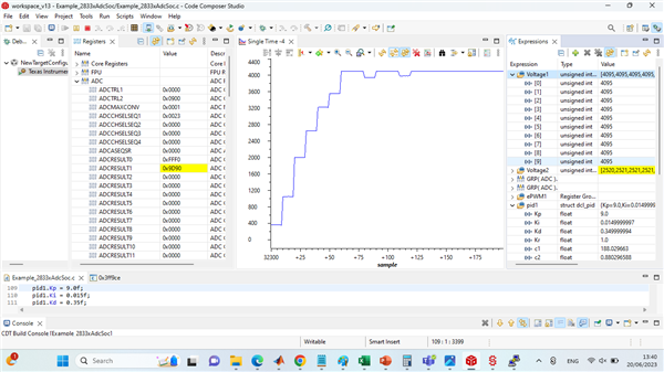
首先:如果 rk =0.25被置位、那么在12位 ADC 值(0-4095)的帮助下以及在代码行342下获得了 YK:
YK=(((float) AdcRegs.ADCRESULT0 - 2048.0f)/ 2047.0f;
Kr 可以介于1和-1之间。 如果(悬空) AdcRegs.ADCRESULT0 介于(4095和0)之间。
现在,下一行345 : Uk = DCL_runPID_C4(&pid1, rk, YS, lk);…… 用于运行 PID 函数。 它提供控制努力值 u (k)。
提问1:问题是 u (k)数值范围的数值是多少???? 请解释第345行。
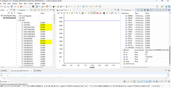
第348行: clampactive = DCL_runClamp_C1 (&uk、upperlim、lowlim);定义上限和下限饱和。
问题2:第350行: LK =(clampactive == 0U)? 1.0f: 0.0f;.. 没有强制选择1或0为 Clampactive。 我们可以选择其中任何一个吗???
对于353-354行:
Duty =(UK / 2.0f + 0.5f)*(float) EPwm1Regs.TBPRD;
EPwm1Regs.CMPA.half.CMPA =(UINT16)占空比;
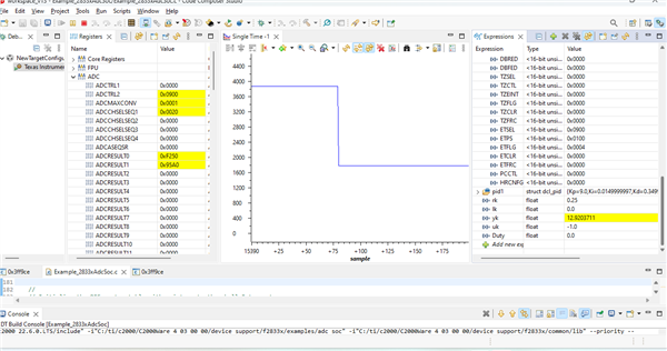
问题3:
F ROM 上面的行、如果已知问题1中的 u (k)、那么为什么要除以2.5 (2.0f+0.5f)、然后乘以 EPwm1Regs.TBPRD? 这个 ePWM 是我们在第286行(EPwm1Regs.TBPRD = 0xFFFF)对 ADC 采样的 ePWM。 如果是、那么如果假设您的 y (k)将会费更改为 ADC 值、上述占空比会如何变化? 我想我应该删除线路309、然后检查 GPIO0或者 GPIO1、如果 y (k)发生变化、那么占空比会发生变化。
//########################################################################### // // FILE: Example_2833xAdcSoc.c // // TITLE: ADC Start of Conversion Example // //! \addtogroup f2833x_example_list //! <h1> ADC Start of Conversion (adc_soc)</h1> //! //! This ADC example uses ePWM1 to generate a periodic ADC SOC on SEQ1. //! Two channels are converted, ADCINA3 and ADCINA2. //! //! \b Watch \b Variables \n //! - Voltage1[10] - Last 10 ADCRESULT0 values //! - Voltage2[10] - Last 10 ADCRESULT1 values //! - ConversionCount - Current result number 0-9 //! - LoopCount - Idle loop counter // //########################################################################### // $TI Release: $ // $Release Date: $ // $Copyright: // Copyright (C) 2009-2023 Texas Instruments Incorporated - http://www.ti.com/ // // Redistribution and use in source and binary forms, with or without // modification, are permitted provided that the following conditions // are met: // // Redistributions of source code must retain the above copyright // notice, this list of conditions and the following disclaimer. // // Redistributions in binary form must reproduce the above copyright // notice, this list of conditions and the following disclaimer in the // documentation and/or other materials provided with the // distribution. // // Neither the name of Texas Instruments Incorporated nor the names of // its contributors may be used to endorse or promote products derived // from this software without specific prior written permission. // // THIS SOFTWARE IS PROVIDED BY THE COPYRIGHT HOLDERS AND CONTRIBUTORS // "AS IS" AND ANY EXPRESS OR IMPLIED WARRANTIES, INCLUDING, BUT NOT // LIMITED TO, THE IMPLIED WARRANTIES OF MERCHANTABILITY AND FITNESS FOR // A PARTICULAR PURPOSE ARE DISCLAIMED. IN NO EVENT SHALL THE COPYRIGHT // OWNER OR CONTRIBUTORS BE LIABLE FOR ANY DIRECT, INDIRECT, INCIDENTAL, // SPECIAL, EXEMPLARY, OR CONSEQUENTIAL DAMAGES (INCLUDING, BUT NOT // LIMITED TO, PROCUREMENT OF SUBSTITUTE GOODS OR SERVICES; LOSS OF USE, // DATA, OR PROFITS; OR BUSINESS INTERRUPTION) HOWEVER CAUSED AND ON ANY // THEORY OF LIABILITY, WHETHER IN CONTRACT, STRICT LIABILITY, OR TORT // (INCLUDING NEGLIGENCE OR OTHERWISE) ARISING IN ANY WAY OUT OF THE USE // OF THIS SOFTWARE, EVEN IF ADVISED OF THE POSSIBILITY OF SUCH DAMAGE. // $ //########################################################################### // // Included Files // #include "DSP28x_Project.h" // Device Headerfile and Examples Include File #include "DSP2833x_Device.h" #include "DSP2833x_Examples.h" #include "DSP2833x_GlobalPrototypes.h" #include "DCLF32.h" // // Function Prototypes // void gpio_select(void); void Setup_ePWM1(void); __interrupt void adc_isr(void); // // Globals // Uint16 LoopCount; Uint16 ConversionCount; Uint16 Voltage1[10]; Uint16 Voltage2[10]; //DCL_PID pid1 = PID_DEFAULTS; //typedef struct dcl_pid pid1; struct dcl_pid pid1; //float pid1; DCL_PID pid1 = PID_DEFAULTS; float32_t yk; float32_t lk; float32_t uk; //float32_t rk = 0.25; // initial value for control reference //float32_t lk = 1.0; // control loop not saturated float32_t rk; // initial value for control reference float32_t lk; // control loop not saturated float Duty; float upperlim = 0.95; float lowerlim = 0.05; unsigned int clampactive; // // Main // void main(void) { //DCL_PID pid1 = PID_DEFAULTS; pid1.Kp = 9.0f; pid1.Ki = 0.015f; pid1.Kd = 0.35f; pid1.Kr = 1.0f; pid1.c1 = 188.0296600613396f; pid1.c2 = 0.880296600613396f; pid1.d2 = 0.0f; pid1.d3 = 0.0f; pid1.i10 = 0.0f; pid1.i14 = 1.0f; pid1.Umax = 1.0f; pid1.Umin = -1.0f; rk = 0.25; // initial value for control reference lk = 1.0; // // Step 1. Initialize System Control: // PLL, WatchDog, enable Peripheral Clocks // This example function is found in the DSP2833x_SysCtrl.c file. // InitSysCtrl(); EALLOW; #if (CPU_FRQ_150MHZ) // Default - 150 MHz SYSCLKOUT // // HSPCLK = SYSCLKOUT/2*ADC_MODCLK2 = 150/(2*3) = 25.0 MHz // #define ADC_MODCLK 0x3 #endif #if (CPU_FRQ_100MHZ) // // HSPCLK = SYSCLKOUT/2*ADC_MODCLK2 = 100/(2*2) = 25.0 MHz // #define ADC_MODCLK 0x2 #endif EDIS; // // Define ADCCLK clock frequency ( less than or equal to 25 MHz ) // Assuming InitSysCtrl() has set SYSCLKOUT to 150 MHz // EALLOW; SysCtrlRegs.HISPCP.all = ADC_MODCLK; EDIS; // // Step 2. Initialize GPIO: // This example function is found in the DSP2833x_Gpio.c file and // illustrates how to set the GPIO to it's default state. // // InitGpio(); // Skipped for this example // // Step 3. Clear all interrupts and initialize PIE vector table: // Disable CPU interrupts // DINT; // // Initialize the PIE control registers to their default state. // The default state is all PIE interrupts disabled and flags // are cleared. // This function is found in the DSP2833x_PieCtrl.c file. // InitPieCtrl(); // // Disable CPU interrupts and clear all CPU interrupt flags: // IER = 0x0000; IFR = 0x0000; // // Initialize the PIE vector table with pointers to the shell Interrupt // Service Routines (ISR). // This will populate the entire table, even if the interrupt // is not used in this example. This is useful for debug purposes. // The shell ISR routines are found in DSP2833x_DefaultIsr.c. // This function is found in DSP2833x_PieVect.c. // InitPieVectTable(); // // Interrupts that are used in this example are re-mapped to // ISR functions found within this file. // EALLOW; // This is needed to write to EALLOW protected register PieVectTable.ADCINT = &adc_isr; EDIS; // This is needed to disable write to EALLOW protected registers //* configure ePWM1 */ EALLOW; SysCtrlRegs.PCLKCR0.bit.TBCLKSYNC = 0; EDIS; //InitEPwm1Gpio(); // [F2806x_EPwm.c] gpio_select(); Setup_ePWM1(); // init ePWM1A //void Setup_ePWM1(void) //{ //EPwm1Regs.TBCTL.bit.CTRMODE = 3; // freeze TB counter //EPwm1Regs.TBCTL.bit.PRDLD = 1; // immediate load //EPwm1Regs.TBCTL.bit.PHSEN = 0; // disable phase loading //EPwm1Regs.TBCTL.bit.SYNCOSEL = 3; // disable SYNCOUT signal //EPwm1Regs.TBCTL.bit.HSPCLKDIV = 0; // TBCLK = SYSCLKOUT //EPwm1Regs.TBCTL.bit.CLKDIV = 0; // clock divider = /1 //EPwm1Regs.TBCTL.bit.FREE_SOFT = 2; // free run on emulation suspend //EPwm1Regs.TBPRD = 0x2328; // set period for ePWM1 (0x2328 = 10kHz) //EPwm1Regs.TBPHS.all = 0; // time-base Phase Register //EPwm1Regs.TBCTR = 0; // time-base Counter Register //EPwm1Regs.ETSEL.bit.SOCAEN = 1; // enable SOC on A group //EPwm1Regs.ETSEL.bit.SOCASEL = 1; // select SOC from zero match //EPwm1Regs.ETPS.bit.SOCAPRD = 1; // generate pulse on 1st event //EPwm1Regs.CMPCTL.bit.SHDWAMODE = 0; // enable shadow mode //EPwm1Regs.CMPCTL.bit.LOADAMODE = 2; // reload on CTR=zero //EPwm1Regs.CMPA.half.CMPA = 0x0080; // set compare A value //EPwm1Regs.AQCTLA.bit.CAU = AQ_SET; // HIGH on CMPA up match //EPwm1Regs.AQCTLA.bit.ZRO = AQ_CLEAR; // LOW on zero match //} EALLOW; SysCtrlRegs.PCLKCR0.bit.TBCLKSYNC = 1; EDIS; // // Step 4. Initialize all the Device Peripherals: // This function is found in DSP2833x_InitPeripherals.c // // InitPeripherals(); // Not required for this example InitAdc(); // For this example, init the ADC // // Step 5. User specific code, enable interrupts: // //gpio_select(); //Setup_ePWM1(); // init ePWM1A,ePWM1B // // Enable ADCINT in PIE // PieCtrlRegs.PIEIER1.bit.INTx6 = 1; IER |= M_INT1; // Enable CPU Interrupt 1 EINT; // Enable Global interrupt INTM ERTM; // Enable Global realtime interrupt DBGM LoopCount = 0; ConversionCount = 0; // // Configure ADC // AdcRegs.ADCMAXCONV.all = 0x0001; // Setup 2 conv's on SEQ1 AdcRegs.ADCCHSELSEQ1.bit.CONV00 = 0x3; // Setup ADCINA3 as 1st SEQ1 conv. AdcRegs.ADCCHSELSEQ1.bit.CONV01 = 0x2; // Setup ADCINA2 as 2nd SEQ1 conv. // // Enable SOCA from ePWM to start SEQ1 // AdcRegs.ADCTRL2.bit.EPWM_SOCA_SEQ1 = 1; AdcRegs.ADCTRL2.bit.INT_ENA_SEQ1 = 1; // Enable SEQ1 interrupt (every EOS) // // Assumes ePWM1 clock is already enabled in InitSysCtrl(); // EPwm1Regs.ETSEL.bit.SOCAEN = 1; // Enable SOC on A group EPwm1Regs.ETSEL.bit.SOCASEL = 4; // Select SOC from from CPMA on upcount EPwm1Regs.ETPS.bit.SOCAPRD = 1; // Generate pulse on 1st event EPwm1Regs.CMPA.half.CMPA = 0x0080; // Set compare A value EPwm1Regs.TBPRD = 0xFFFF; // Set period for ePWM1 EPwm1Regs.TBCTL.bit.CTRMODE = 0; // count up and start // // Wait for ADC interrupt // for(;;) { LoopCount++; } } // void Setup_ePWM1(void) { EPwm1Regs.TBCTL.bit.CTRMODE = 3; // freeze TB counter EPwm1Regs.TBCTL.bit.PRDLD = 1; // immediate load EPwm1Regs.TBCTL.bit.PHSEN = 0; // disable phase loading EPwm1Regs.TBCTL.bit.SYNCOSEL = 3; // disable SYNCOUT signal EPwm1Regs.TBCTL.bit.HSPCLKDIV = 0; // TBCLK = SYSCLKOUT EPwm1Regs.TBCTL.bit.CLKDIV = 0; // clock divider = /1 EPwm1Regs.TBCTL.bit.FREE_SOFT = 2; // free run on emulation suspend EPwm1Regs.TBPRD = 0x2328; // set period for ePWM1 (0x2328 = 10kHz) EPwm1Regs.TBPHS.all = 0; // time-base Phase Register EPwm1Regs.TBCTR = 0; // time-base Counter Register EPwm1Regs.ETSEL.bit.SOCAEN = 1; // enable SOC on A group EPwm1Regs.ETSEL.bit.SOCASEL = 1; // select SOC from zero match EPwm1Regs.ETPS.bit.SOCAPRD = 1; // generate pulse on 1st event EPwm1Regs.CMPCTL.bit.SHDWAMODE = 0; // enable shadow mode EPwm1Regs.CMPCTL.bit.LOADAMODE = 2; // reload on CTR=zero EPwm1Regs.CMPA.half.CMPA = 0x0080; // set compare A value EPwm1Regs.AQCTLA.bit.CAU = AQ_SET; // HIGH on CMPA up match EPwm1Regs.AQCTLA.bit.ZRO = AQ_CLEAR; // LOW on zero match } void gpio_select(void) { EALLOW; GpioCtrlRegs.GPAPUD.bit.GPIO0 = 0; // Enable pullup on GPIO0 GpioCtrlRegs.GPAPUD.bit.GPIO1 = 0; // Enable pullup on GPIO1 GpioCtrlRegs.GPAMUX1.bit.GPIO0 = 1; // GPIO0 = PWM1A GpioCtrlRegs.GPAMUX1.bit.GPIO1 = 1; // GPIO0 = PWM1B EDIS; } // adc_isr - // __interrupt void adc_isr(void) { Voltage1[ConversionCount] = AdcRegs.ADCRESULT0 >>4; Voltage2[ConversionCount] = AdcRegs.ADCRESULT1 >>4; // read ADC channel yk = ((float) AdcRegs.ADCRESULT0 - 2048.0f) / 2047.0f; // run PID controller uk = DCL_runPID_C4(&pid1, rk, yk, lk); // external clamp for anti-windup reset clampactive = DCL_runClamp_C1(&uk, upperlim, lowerlim); //clampactive = DCL_runClamp_C1(&uk, Umax, Umin); lk = (clampactive == 0U) ? 1.0f : 0.0f; // write u(k) to PWM Duty = (uk / 2.0f + 0.5f) * (float) EPwm1Regs.TBPRD; EPwm1Regs.CMPA.half.CMPA = (Uint16) Duty; // // If 40 conversions have been logged, start over // if(ConversionCount == 9) { ConversionCount = 0; } else { ConversionCount++; } // // Reinitialize for next ADC sequence // AdcRegs.ADCTRL2.bit.RST_SEQ1 = 1; // Reset SEQ1 AdcRegs.ADCST.bit.INT_SEQ1_CLR = 1; // Clear INT SEQ1 bit PieCtrlRegs.PIEACK.all = PIEACK_GROUP1; // Acknowledge interrupt to PIE return; } // // End of File //
请分步解释所有问题。 抱歉、我不熟悉 DCL PID 仿真。
谢谢
此致
阿尔萨兰
尊敬的 Arsalan:
对于 Q1、PID 控制器还具有一个在122&123行设置的内部钳位、因此输出范围将钳位到1.0 ~-1.0
对于第二季度,我不是完全确定你的意思是"没有强迫选择1或0为 clampactive ". 该外部钳位的目的是确保控制器不会因饱和响应而发生过阻尼(如果控制力度被钳制)、因此不会因反馈环路的影响而恢复。 我们的示例仅实施了基本的响应、允许100%的反馈或0%的反馈、如图所示、lk 表示输入控制器的反馈比率:
您可以随意更改周围的值、实际上、该外部钳位是不必要的、因为 PID 控制器还包括一个内部钳位。 我认为该钳位的目的仅是展示 Lk 何时被钳位。 指的是 DCL_PID_C3的代码实现、它是 ASM C4的内联 C 版本。
对于 Q3、我必须联系我们的 C2000 PWM 导出、以便具体回答我们为何要将其除以2.5。 但我认为您需要进行一些清理、因为您有多个 EPwm1Regs 初始化实例。 一旦我收到来自内部出口部门的反馈、我们会稍后回复您。
此致!
王森
尊敬的 Seng:
感谢您提供的背景信息。 对我来说非常有帮助。 我将等待您对2.5部分的进一步反馈。
昨天、我在硬件上测试了代码。 我总结一下这里的结果:信号被施加在 ADCINA3上作为0 - 3V 设置的输入( 见图1 )
因此、我在这里绘制了 电压1图 :给出一个大约243的值。 在 0.1V ADCINA3作为输入电压 和 TBPRD 0xFFFF ( 参阅 图2 )。
图3 显示了所有 DCL 值参数(KP、ki、Kd、C1、C2、D1、D2.、VMAX、Vmin 等)。 此处、Rk = 0.25、Lk =0、YK=0.9、UK = 0.05、占空比= 34405.875、 0.1V ADCINA3作为输入电压
图1 :
图2:
图3:
在升高 输入电压 ADCINA3 从0.1V 缓慢 变化至3V、中以表格形式列出了结果 图片4和图片5 。
电压1图 :图4中给出了一个大约4095的值。 在 Picture5中、rk = 0.25、lk =0、YK=30.9、UK = 0.05、占空比= 34405.875、 3V ADCINA3作为输入电压
图4:
图5:
问题1:
没有电源时。 全部接地、示波器上的占空比为2.4%。 当电源接通时,占空比为48%。 随着输入电压 ADCINA3的增加、占空比编号34405.875 (图5)没有变化。 它保持不变、为什么呢? 我想它应该会根据施加的电压变化来改变占空比。 因为我 会将该占空比发送到其中一个 ePWM GPIO 端口、以通过示波器观察结果、从而检查占空比是否会随施加的输入电压的增大而变化。 请对此进行解释。 我按照此设置在我的硬件上进行构建:
问题2:
如上图所示、当将电压从0V 增加到3V ADCINA3作为输入电压时、y (k)从0.9增加到30.9。
在 DCL 指南的 "示例5:在 FPU32上运行的 PID 控制器"中、y (k)必须在稳定后等于 r (k)。 因此、在这里、增加了输入 ADCINA3电压后、图5显示了小延迟后的稳定输出、但 y (k)不等于基准电压 r (k)。 请说明。
问题3:
C1和 C2是滤波器系数,但 D2和 D3与 I10和 i14相同? 我们可以说它们是延迟后的系数吗? 上图中、在增大电压时只有 D2和 D3发生变化、为什么? 请说明。
此处附有代码: ( 此处删除了多 EPwm1Regs 初始化)
//########################################################################### // // FILE: Example_2833xAdcSoc.c // // TITLE: ADC Start of Conversion Example // //! \addtogroup f2833x_example_list //! <h1> ADC Start of Conversion (adc_soc)</h1> //! //! This ADC example uses ePWM1 to generate a periodic ADC SOC on SEQ1. //! Two channels are converted, ADCINA3 and ADCINA2. //! //! \b Watch \b Variables \n //! - Voltage1[10] - Last 10 ADCRESULT0 values //! - Voltage2[10] - Last 10 ADCRESULT1 values //! - ConversionCount - Current result number 0-9 //! - LoopCount - Idle loop counter // //########################################################################### // $TI Release: $ // $Release Date: $ // $Copyright: // Copyright (C) 2009-2023 Texas Instruments Incorporated - http://www.ti.com/ // // Redistribution and use in source and binary forms, with or without // modification, are permitted provided that the following conditions // are met: // // Redistributions of source code must retain the above copyright // notice, this list of conditions and the following disclaimer. // // Redistributions in binary form must reproduce the above copyright // notice, this list of conditions and the following disclaimer in the // documentation and/or other materials provided with the // distribution. // // Neither the name of Texas Instruments Incorporated nor the names of // its contributors may be used to endorse or promote products derived // from this software without specific prior written permission. // // THIS SOFTWARE IS PROVIDED BY THE COPYRIGHT HOLDERS AND CONTRIBUTORS // "AS IS" AND ANY EXPRESS OR IMPLIED WARRANTIES, INCLUDING, BUT NOT // LIMITED TO, THE IMPLIED WARRANTIES OF MERCHANTABILITY AND FITNESS FOR // A PARTICULAR PURPOSE ARE DISCLAIMED. IN NO EVENT SHALL THE COPYRIGHT // OWNER OR CONTRIBUTORS BE LIABLE FOR ANY DIRECT, INDIRECT, INCIDENTAL, // SPECIAL, EXEMPLARY, OR CONSEQUENTIAL DAMAGES (INCLUDING, BUT NOT // LIMITED TO, PROCUREMENT OF SUBSTITUTE GOODS OR SERVICES; LOSS OF USE, // DATA, OR PROFITS; OR BUSINESS INTERRUPTION) HOWEVER CAUSED AND ON ANY // THEORY OF LIABILITY, WHETHER IN CONTRACT, STRICT LIABILITY, OR TORT // (INCLUDING NEGLIGENCE OR OTHERWISE) ARISING IN ANY WAY OUT OF THE USE // OF THIS SOFTWARE, EVEN IF ADVISED OF THE POSSIBILITY OF SUCH DAMAGE. // $ //########################################################################### // // Included Files // #include "DSP28x_Project.h" // Device Headerfile and Examples Include File #include "DSP2833x_Device.h" #include "DSP2833x_Examples.h" #include "DSP2833x_GlobalPrototypes.h" #include "DCLF32.h" // // Function Prototypes // void gpio_select(void); void Setup_ePWM1(void); __interrupt void adc_isr(void); // // Globals // Uint16 LoopCount; Uint16 ConversionCount; Uint16 Voltage1[10]; Uint16 Voltage2[10]; //typedef struct dcl_pid pid1; struct dcl_pid pid1; //DCL_PID pid1 = PID_DEFAULTS; DCL_PID pid1 = PID_DEFAULTS; float32_t yk; float32_t lk; float32_t uk; float32_t rk; // initial value for control reference float32_t lk; // control loop not saturated float Duty; float upperlim = 0.95; float lowerlim = 0.05; unsigned int clampactive; // // Main // void main(void) { pid1.Kp = 9.0f; pid1.Ki = 0.015f; pid1.Kd = 0.35f; pid1.Kr = 1.0f; pid1.c1 = 188.0296600613396f; pid1.c2 = 0.880296600613396f; pid1.d2 = 0.0f; pid1.d3 = 0.0f; pid1.i10 = 0.0f; pid1.i14 = 1.0f; pid1.Umax = 1.0f; pid1.Umin = -1.0f; rk = 0.25; // initial value for control reference lk = 1.0; // control loop not saturated // // Step 1. Initialize System Control: // PLL, WatchDog, enable Peripheral Clocks // This example function is found in the DSP2833x_SysCtrl.c file. // InitSysCtrl(); EALLOW; #if (CPU_FRQ_150MHZ) // Default - 150 MHz SYSCLKOUT // // HSPCLK = SYSCLKOUT/2*ADC_MODCLK2 = 150/(2*3) = 25.0 MHz // #define ADC_MODCLK 0x3 #endif #if (CPU_FRQ_100MHZ) // // HSPCLK = SYSCLKOUT/2*ADC_MODCLK2 = 100/(2*2) = 25.0 MHz // #define ADC_MODCLK 0x2 #endif EDIS; // // Define ADCCLK clock frequency ( less than or equal to 25 MHz ) // Assuming InitSysCtrl() has set SYSCLKOUT to 150 MHz // EALLOW; SysCtrlRegs.HISPCP.all = ADC_MODCLK; EDIS; // // Step 2. Initialize GPIO: // This example function is found in the DSP2833x_Gpio.c file and // illustrates how to set the GPIO to it's default state. // // InitGpio(); // Skipped for this example // // Step 3. Clear all interrupts and initialize PIE vector table: // Disable CPU interrupts // DINT; // // Initialize the PIE control registers to their default state. // The default state is all PIE interrupts disabled and flags // are cleared. // This function is found in the DSP2833x_PieCtrl.c file. // InitPieCtrl(); // // Disable CPU interrupts and clear all CPU interrupt flags: // IER = 0x0000; IFR = 0x0000; // // Initialize the PIE vector table with pointers to the shell Interrupt // Service Routines (ISR). // This will populate the entire table, even if the interrupt // is not used in this example. This is useful for debug purposes. // The shell ISR routines are found in DSP2833x_DefaultIsr.c. // This function is found in DSP2833x_PieVect.c. // InitPieVectTable(); // // Interrupts that are used in this example are re-mapped to // ISR functions found within this file. // EALLOW; // This is needed to write to EALLOW protected register PieVectTable.ADCINT = &adc_isr; EDIS; // This is needed to disable write to EALLOW protected registers //* configure ePWM1 */ EALLOW; SysCtrlRegs.PCLKCR0.bit.TBCLKSYNC = 0; EDIS; //InitEPwm1Gpio(); // [F2806x_EPwm.c] gpio_select(); Setup_ePWM1(); // init ePWM1A EALLOW; SysCtrlRegs.PCLKCR0.bit.TBCLKSYNC = 1; EDIS; // // Step 4. Initialize all the Device Peripherals: // This function is found in DSP2833x_InitPeripherals.c // // InitPeripherals(); // Not required for this example InitAdc(); // For this example, init the ADC // // Step 5. User specific code, enable interrupts: // // // Enable ADCINT in PIE // PieCtrlRegs.PIEIER1.bit.INTx6 = 1; IER |= M_INT1; // Enable CPU Interrupt 1 EINT; // Enable Global interrupt INTM ERTM; // Enable Global realtime interrupt DBGM LoopCount = 0; ConversionCount = 0; // // Configure ADC // AdcRegs.ADCMAXCONV.all = 0x0001; // Setup 2 conv's on SEQ1 AdcRegs.ADCCHSELSEQ1.bit.CONV00 = 0x3; // Setup ADCINA3 as 1st SEQ1 conv. AdcRegs.ADCCHSELSEQ1.bit.CONV01 = 0x2; // Setup ADCINA2 as 2nd SEQ1 conv. // // Enable SOCA from ePWM to start SEQ1 // AdcRegs.ADCTRL2.bit.EPWM_SOCA_SEQ1 = 1; AdcRegs.ADCTRL2.bit.INT_ENA_SEQ1 = 1; // Enable SEQ1 interrupt (every EOS) // // Assumes ePWM1 clock is already enabled in InitSysCtrl(); // // Wait for ADC interrupt // for(;;) { LoopCount++; } } // void Setup_ePWM1(void) { //EPwm1Regs.TBCTL.bit.CTRMODE = 3; // freeze TB counter EPwm1Regs.TBCTL.bit.CTRMODE = 0; // count up and start EPwm1Regs.TBCTL.bit.PRDLD = 1; // immediate load EPwm1Regs.TBCTL.bit.PHSEN = 0; // disable phase loading EPwm1Regs.TBCTL.bit.SYNCOSEL = 3; // disable SYNCOUT signal EPwm1Regs.TBCTL.bit.HSPCLKDIV = 0; // TBCLK = SYSCLKOUT EPwm1Regs.TBCTL.bit.CLKDIV = 0; // clock divider = /1 EPwm1Regs.TBCTL.bit.FREE_SOFT = 2; // free run on emulation suspend //EPwm1Regs.TBPRD = 0x2328; // set period for ePWM1 (0x2328 = 10kHz) EPwm1Regs.TBPRD = 0xFFFF; // set period for ePWM1 (0x2328 = 10kHz) EPwm1Regs.TBPHS.all = 0; // time-base Phase Register EPwm1Regs.TBCTR = 0; // time-base Counter Register EPwm1Regs.ETSEL.bit.SOCAEN = 1; // enable SOC on A group //EPwm1Regs.ETSEL.bit.SOCASEL = 1; // select SOC from zero match EPwm1Regs.ETSEL.bit.SOCASEL = 1; // select SOC from zero match //EPwm1Regs.ETSEL.bit.SOCASEL = 4; // select SOC from zero match EPwm1Regs.ETPS.bit.SOCAPRD = 1; // generate pulse on 1st event EPwm1Regs.CMPCTL.bit.SHDWAMODE = 0; // enable shadow mode EPwm1Regs.CMPCTL.bit.LOADAMODE = 2; // reload on CTR=zero EPwm1Regs.CMPA.half.CMPA = 0x0080; // set compare A value EPwm1Regs.AQCTLA.bit.CAU = AQ_SET; // HIGH on CMPA up match EPwm1Regs.AQCTLA.bit.ZRO = AQ_CLEAR; // LOW on zero match } void gpio_select(void) { EALLOW; GpioCtrlRegs.GPAPUD.bit.GPIO0 = 0; // Enable pullup on GPIO0 GpioCtrlRegs.GPAPUD.bit.GPIO1 = 0; // Enable pullup on GPIO1 GpioCtrlRegs.GPAMUX1.bit.GPIO0 = 1; // GPIO0 = PWM1A GpioCtrlRegs.GPAMUX1.bit.GPIO1 = 1; // GPIO0 = PWM1B EDIS; } // adc_isr - // __interrupt void adc_isr(void) { Voltage1[ConversionCount] = AdcRegs.ADCRESULT0 >>4; Voltage2[ConversionCount] = AdcRegs.ADCRESULT1 >>4; // read ADC channel yk = ((float) AdcRegs.ADCRESULT0 - 2048.0f) / 2047.0f; // run PID controller uk = DCL_runPID_C4(&pid1, rk, yk, lk); // external clamp for anti-windup reset clampactive = DCL_runClamp_C1(&uk, upperlim, lowerlim); //clampactive = DCL_runClamp_C1(&uk, Umax, Umin); lk = (clampactive == 0U) ? 1.0f : 0.0f; // write u(k) to PWM Duty = (uk / 2.0f + 0.5f) * (float) EPwm1Regs.TBPRD; EPwm1Regs.CMPA.half.CMPA = (Uint16) Duty; // // If 40 conversions have been logged, start over // if(ConversionCount == 9) { ConversionCount = 0; } else { ConversionCount++; } // // Reinitialize for next ADC sequence // AdcRegs.ADCTRL2.bit.RST_SEQ1 = 1; // Reset SEQ1 AdcRegs.ADCST.bit.INT_SEQ1_CLR = 1; // Clear INT SEQ1 bit PieCtrlRegs.PIEACK.all = PIEACK_GROUP1; // Acknowledge interrupt to PIE return; } // // End of File //
谢谢
此致
阿尔萨兰
我将等待您对2.5部门的进一步反馈。
尊敬的 Arsalan:
这一行不能除以2.5f。 相反、它由以下主题进行解释: e2e.ti.com/.../ccs-tms320f28379d-dcl-c200-motorware
"针对第一个问题、该示例中的假设是将控制器输出标准化为+/-1.0f。 代码行进行缩放、然后偏移控制器输出、使其在0 - 1.0f 的范围内、再乘以 PWM 周期以获得占空比。 这只是一个代码示例。"
此致、
马瑞安
您好、Arsalan、很抱歉耽误了时间。
正如 Ryan 所说、UK/2.0f + 0.5f 是尝试将控制输出范围从-1.0~1.0f 标准化到0~1.0f、表示占空比的0%至100%。
从您的代码来看、您已经在 F28335上设置了 ADCINA2、ADCINA3、但 ISR 仍在从 F28069 DCL 示例中读取 ADCRESULT0、向 ADCINA3提供信号不应对 ADCRESULT0产生任何影响、ADCRESULT0和 PID 的所有后续更改都可能是由于电压浮动造成的。
有一点我忘记提到了、那就是还有一个外部饱和、用于将饱和范围进一步钳位到0.05f~0.95f、而不是+/-1.0f。 因此、如果不需要额外的饱和、您可以注释掉第315行的 runClamp_C1。
此致!
王森
您好、Ryan、
感谢您的答复。 我会在落实您的建议后很快回复您。 我很快就会告诉你结果。
此致
阿尔萨兰
尊敬的 Sen:
感谢您的答复。 我会在落实您的建议后很快回复您。 我很快就会告诉你结果。
此致
阿尔萨兰
我们将等待您的结果。
此致!
马瑞安
尊敬的 Sen 和 Ryan:
感谢您的全面回复。 非常有帮助
从您的代码来看、您已经在 F28335上设置了 ADCINA2、ADCINA3、但 ISR 仍在从 F28069 DCL 示例中读取 ADCRESULT0、向 ADCINA3提供信号不应对 ADCRESULT0产生任何影响、ADCRESULT0和 PID 的所有后续更改都可能是由于电压浮动造成的。
正如建议的那样、我修复了这个问题、现在我在 ADCINA0上进行应用、并且 ISR 正在读取 ADCRESULT。 它仅以2个值读取占空比。 (6553.5或0)、温度分别为0V 和3V。 我将电压设为1.2V、占空比设为0时、不会得出中间值(周围没有中间值)。 参见图。 以下内容:
在应用于 ADCINA0上0V (接地)时、输出电压1 = 0在观察窗口上大约为65535、(因为 TBPRD = FFFF)请参见图1、2、并且当应用3V 时、占空比显示0图3、4。
图5显示、当我在 ADCINA0上施加了大约1.2的电压时、占空比不会显示在中间值附近。 它会保持为0。 占空比必须根据施加的任何电压而变化。
画面1 (0V 时)
Picture2 (0V 时)--占空比= 65535
画面3 (3V 时)
图4 (3V 时)--占空比= 0
图5 (1.2V 时大约)... 占空比没有中间值。 它会保持为0。
更新的代码附在此处
//########################################################################### // // FILE: Example_2833xAdcSoc.c // // TITLE: ADC Start of Conversion Example // //! \addtogroup f2833x_example_list //! <h1> ADC Start of Conversion (adc_soc)</h1> //! //! This ADC example uses ePWM1 to generate a periodic ADC SOC on SEQ1. //! Two channels are converted, ADCINA3 and ADCINA2. //! //! \b Watch \b Variables \n //! - Voltage1[10] - Last 10 ADCRESULT0 values //! - Voltage2[10] - Last 10 ADCRESULT1 values //! - ConversionCount - Current result number 0-9 //! - LoopCount - Idle loop counter // //########################################################################### // $TI Release: $ // $Release Date: $ // $Copyright: // Copyright (C) 2009-2023 Texas Instruments Incorporated - http://www.ti.com/ // // Redistribution and use in source and binary forms, with or without // modification, are permitted provided that the following conditions // are met: // // Redistributions of source code must retain the above copyright // notice, this list of conditions and the following disclaimer. // // Redistributions in binary form must reproduce the above copyright // notice, this list of conditions and the following disclaimer in the // documentation and/or other materials provided with the // distribution. // // Neither the name of Texas Instruments Incorporated nor the names of // its contributors may be used to endorse or promote products derived // from this software without specific prior written permission. // // THIS SOFTWARE IS PROVIDED BY THE COPYRIGHT HOLDERS AND CONTRIBUTORS // "AS IS" AND ANY EXPRESS OR IMPLIED WARRANTIES, INCLUDING, BUT NOT // LIMITED TO, THE IMPLIED WARRANTIES OF MERCHANTABILITY AND FITNESS FOR // A PARTICULAR PURPOSE ARE DISCLAIMED. IN NO EVENT SHALL THE COPYRIGHT // OWNER OR CONTRIBUTORS BE LIABLE FOR ANY DIRECT, INDIRECT, INCIDENTAL, // SPECIAL, EXEMPLARY, OR CONSEQUENTIAL DAMAGES (INCLUDING, BUT NOT // LIMITED TO, PROCUREMENT OF SUBSTITUTE GOODS OR SERVICES; LOSS OF USE, // DATA, OR PROFITS; OR BUSINESS INTERRUPTION) HOWEVER CAUSED AND ON ANY // THEORY OF LIABILITY, WHETHER IN CONTRACT, STRICT LIABILITY, OR TORT // (INCLUDING NEGLIGENCE OR OTHERWISE) ARISING IN ANY WAY OUT OF THE USE // OF THIS SOFTWARE, EVEN IF ADVISED OF THE POSSIBILITY OF SUCH DAMAGE. // $ //########################################################################### // // Included Files // #include "DSP28x_Project.h" // Device Headerfile and Examples Include File #include "DSP2833x_Device.h" #include "DSP2833x_Examples.h" #include "DSP2833x_GlobalPrototypes.h" #include "DCLF32.h" // // Function Prototypes // void gpio_select(void); void Setup_ePWM1(void); __interrupt void adc_isr(void); // // Globals // Uint16 LoopCount; Uint16 ConversionCount; Uint16 Voltage1[10]; Uint16 Voltage2[10]; //typedef struct dcl_pid pid1; struct dcl_pid pid1; //DCL_PID pid1 = PID_DEFAULTS; DCL_PID pid1 = PID_DEFAULTS; float32_t yk; float32_t lk; float32_t uk; float32_t rk; // initial value for control reference float32_t lk; // control loop not saturated float Duty; float upperlim = 0.95; float lowerlim = 0.05; unsigned int clampactive; // // Main // void main(void) { pid1.Kp = 9.0f; pid1.Ki = 0.015f; pid1.Kd = 0.35f; pid1.Kr = 1.0f; pid1.c1 = 188.0296600613396f; pid1.c2 = 0.880296600613396f; pid1.d2 = 0.0f; pid1.d3 = 0.0f; pid1.i10 = 0.0f; pid1.i14 = 1.0f; pid1.Umax = 1.0f; pid1.Umin = -1.0f; rk = 0.25; // initial value for control reference lk = 1.0; // control loop not saturated // // Step 1. Initialize System Control: // PLL, WatchDog, enable Peripheral Clocks // This example function is found in the DSP2833x_SysCtrl.c file. // InitSysCtrl(); EALLOW; #if (CPU_FRQ_150MHZ) // Default - 150 MHz SYSCLKOUT // // HSPCLK = SYSCLKOUT/2*ADC_MODCLK2 = 150/(2*3) = 25.0 MHz // #define ADC_MODCLK 0x3 #endif #if (CPU_FRQ_100MHZ) // // HSPCLK = SYSCLKOUT/2*ADC_MODCLK2 = 100/(2*2) = 25.0 MHz // #define ADC_MODCLK 0x2 #endif EDIS; // // Define ADCCLK clock frequency ( less than or equal to 25 MHz ) // Assuming InitSysCtrl() has set SYSCLKOUT to 150 MHz // EALLOW; SysCtrlRegs.HISPCP.all = ADC_MODCLK; EDIS; // // Step 2. Initialize GPIO: // This example function is found in the DSP2833x_Gpio.c file and // illustrates how to set the GPIO to it's default state. // // InitGpio(); // Skipped for this example // // Step 3. Clear all interrupts and initialize PIE vector table: // Disable CPU interrupts // DINT; // // Initialize the PIE control registers to their default state. // The default state is all PIE interrupts disabled and flags // are cleared. // This function is found in the DSP2833x_PieCtrl.c file. // InitPieCtrl(); // // Disable CPU interrupts and clear all CPU interrupt flags: // IER = 0x0000; IFR = 0x0000; // // Initialize the PIE vector table with pointers to the shell Interrupt // Service Routines (ISR). // This will populate the entire table, even if the interrupt // is not used in this example. This is useful for debug purposes. // The shell ISR routines are found in DSP2833x_DefaultIsr.c. // This function is found in DSP2833x_PieVect.c. // InitPieVectTable(); // // Interrupts that are used in this example are re-mapped to // ISR functions found within this file. // EALLOW; // This is needed to write to EALLOW protected register PieVectTable.ADCINT = &adc_isr; EDIS; // This is needed to disable write to EALLOW protected registers //* configure ePWM1 */ EALLOW; SysCtrlRegs.PCLKCR0.bit.TBCLKSYNC = 0; EDIS; //InitEPwm1Gpio(); // [F2806x_EPwm.c] gpio_select(); Setup_ePWM1(); // init ePWM1A EALLOW; SysCtrlRegs.PCLKCR0.bit.TBCLKSYNC = 1; EDIS; // // Step 4. Initialize all the Device Peripherals: // This function is found in DSP2833x_InitPeripherals.c // // InitPeripherals(); // Not required for this example InitAdc(); // For this example, init the ADC // // Step 5. User specific code, enable interrupts: // // // Enable ADCINT in PIE // PieCtrlRegs.PIEIER1.bit.INTx6 = 1; IER |= M_INT1; // Enable CPU Interrupt 1 EINT; // Enable Global interrupt INTM ERTM; // Enable Global realtime interrupt DBGM LoopCount = 0; ConversionCount = 0; // // Configure ADC // AdcRegs.ADCMAXCONV.all = 0x0001; // Setup 2 conv's on SEQ1 AdcRegs.ADCCHSELSEQ1.bit.CONV00 = 0x0; // Setup ADCINA0 as 1st SEQ1 conv. AdcRegs.ADCCHSELSEQ1.bit.CONV01 = 0x2; // Setup ADCINA2 as 2nd SEQ1 conv. // // Enable SOCA from ePWM to start SEQ1 // AdcRegs.ADCTRL2.bit.EPWM_SOCA_SEQ1 = 1; AdcRegs.ADCTRL2.bit.INT_ENA_SEQ1 = 1; // Enable SEQ1 interrupt (every EOS) // // Assumes ePWM1 clock is already enabled in InitSysCtrl(); // // Wait for ADC interrupt // for(;;) { LoopCount++; } } // void Setup_ePWM1(void) { //EPwm1Regs.TBCTL.bit.CTRMODE = 3; // freeze TB counter EPwm1Regs.TBCTL.bit.CTRMODE = 0; // count up and start EPwm1Regs.TBCTL.bit.PRDLD = 1; // immediate load EPwm1Regs.TBCTL.bit.PHSEN = 0; // disable phase loading EPwm1Regs.TBCTL.bit.SYNCOSEL = 3; // disable SYNCOUT signal EPwm1Regs.TBCTL.bit.HSPCLKDIV = 0; // TBCLK = SYSCLKOUT EPwm1Regs.TBCTL.bit.CLKDIV = 0; // clock divider = /1 EPwm1Regs.TBCTL.bit.FREE_SOFT = 2; // free run on emulation suspend //EPwm1Regs.TBPRD = 0x2328; // set period for ePWM1 (0x2328 = 10kHz) EPwm1Regs.TBPRD = 0xFFFF; // set period for ePWM1 (0x2328 = 10kHz) EPwm1Regs.TBPHS.all = 0; // time-base Phase Register EPwm1Regs.TBCTR = 0; // time-base Counter Register EPwm1Regs.ETSEL.bit.SOCAEN = 1; // enable SOC on A group //EPwm1Regs.ETSEL.bit.SOCASEL = 1; // select SOC from zero match EPwm1Regs.ETSEL.bit.SOCASEL = 1; // select SOC from zero match //EPwm1Regs.ETSEL.bit.SOCASEL = 4; // select SOC from zero match EPwm1Regs.ETPS.bit.SOCAPRD = 1; // generate pulse on 1st event EPwm1Regs.CMPCTL.bit.SHDWAMODE = 0; // enable shadow mode EPwm1Regs.CMPCTL.bit.LOADAMODE = 2; // reload on CTR=zero EPwm1Regs.CMPA.half.CMPA = 0x0080; // set compare A value EPwm1Regs.AQCTLA.bit.CAU = AQ_SET; // HIGH on CMPA up match EPwm1Regs.AQCTLA.bit.ZRO = AQ_CLEAR; // LOW on zero match } void gpio_select(void) { EALLOW; GpioCtrlRegs.GPAPUD.bit.GPIO0 = 0; // Enable pullup on GPIO0 GpioCtrlRegs.GPAPUD.bit.GPIO1 = 0; // Enable pullup on GPIO1 GpioCtrlRegs.GPAMUX1.bit.GPIO0 = 1; // GPIO0 = PWM1A GpioCtrlRegs.GPAMUX1.bit.GPIO1 = 1; // GPIO0 = PWM1B EDIS; } // adc_isr - // __interrupt void adc_isr(void) { Voltage1[ConversionCount] = AdcRegs.ADCRESULT0 >>4; Voltage2[ConversionCount] = AdcRegs.ADCRESULT1 >>4; // read ADC channel yk = ((float) AdcRegs.ADCRESULT0 - 2048.0f) / 2047.0f; // run PID controller uk = DCL_runPID_C4(&pid1, rk, yk, lk); // external clamp for anti-windup reset //clampactive = DCL_runClamp_C1(&uk, upperlim, lowerlim); //clampactive = DCL_runClamp_C1(&uk, Umax, Umin); lk = (clampactive == 0U) ? 1.0f : 0.0f; // write u(k) to PWM Duty = (uk / 2.0f + 0.5f) * (float) EPwm1Regs.TBPRD; EPwm1Regs.CMPA.half.CMPA = (Uint16) Duty; // // If 40 conversions have been logged, start over // if(ConversionCount == 9) { ConversionCount = 0; } else { ConversionCount++; } // // Reinitialize for next ADC sequence // AdcRegs.ADCTRL2.bit.RST_SEQ1 = 1; // Reset SEQ1 AdcRegs.ADCST.bit.INT_SEQ1_CLR = 1; // Clear INT SEQ1 bit PieCtrlRegs.PIEACK.all = PIEACK_GROUP1; // Acknowledge interrupt to PIE return; } // // End of File //
请 相应地建议此问题
谢谢
此致
阿尔萨兰
尊敬的 Arsalan:
您现在看到的是正确的 ADC 样本、对吗? 电压似乎为1.2V 时、UK 为-1、这是不正确的、我认为应该为0? 这样、占空比为 TBPRD 的50%。 为什么在1.2V 时、英国为-1V、我认为英国返回的浮点值不正确。 王森 在这里有什么缺失吗?
此致!
马瑞安
尊敬的 Arsalan:
是的,对于一个因第309行而被限定为+/-1的 YK,但在图5中则是12.8。 当 KP 为9.0f 时、控制器会返回最大控制力度、范围为+/-1、这可能会解释为什么占空比只显示为0或100%。 控制器对大于/小于预期输入的响应过大、因此输出了最大的控制力度。
此致!
王森
尊敬的 Seng:
感谢您的答复。
对于其中一个,YK 的值应限定为+/-1
正如您所说的,YK 的值应该是1或-1。 但是根据下面的公式行309、这个值应该在-1到+1之间、包含+1和-1。 它们之间可以是任意值、具体取决于0 - 3V 范围内的 ADC 输入 ADCINA0。
当 KP 为9.0f 时、控制器会返回最大控制力度、范围为+/-1、这可能会解释为何占空比仅为0或100%
我是否应该更改 KP 以便能够在(0到100%)之间更改占空比?? 不完全是0或100%。 因为此处的目的是根据我的 ADC 输入生成不同的占空比。 正如 Ryan 所说的、如果我施加1.2V 电压、那么我的占空比必须接近50%。 您能否请我如何生成不同的占空比、如10、20、50、55、68、77、90 %等??? 是否应该在程序中设置其他参数
代码附在此处
//########################################################################### // // FILE: Example_2833xAdcSoc.c // // TITLE: ADC Start of Conversion Example // //! \addtogroup f2833x_example_list //! <h1> ADC Start of Conversion (adc_soc)</h1> //! //! This ADC example uses ePWM1 to generate a periodic ADC SOC on SEQ1. //! Two channels are converted, ADCINA3 and ADCINA2. //! //! \b Watch \b Variables \n //! - Voltage1[10] - Last 10 ADCRESULT0 values //! - Voltage2[10] - Last 10 ADCRESULT1 values //! - ConversionCount - Current result number 0-9 //! - LoopCount - Idle loop counter // //########################################################################### // $TI Release: $ // $Release Date: $ // $Copyright: // Copyright (C) 2009-2023 Texas Instruments Incorporated - http://www.ti.com/ // // Redistribution and use in source and binary forms, with or without // modification, are permitted provided that the following conditions // are met: // // Redistributions of source code must retain the above copyright // notice, this list of conditions and the following disclaimer. // // Redistributions in binary form must reproduce the above copyright // notice, this list of conditions and the following disclaimer in the // documentation and/or other materials provided with the // distribution. // // Neither the name of Texas Instruments Incorporated nor the names of // its contributors may be used to endorse or promote products derived // from this software without specific prior written permission. // // THIS SOFTWARE IS PROVIDED BY THE COPYRIGHT HOLDERS AND CONTRIBUTORS // "AS IS" AND ANY EXPRESS OR IMPLIED WARRANTIES, INCLUDING, BUT NOT // LIMITED TO, THE IMPLIED WARRANTIES OF MERCHANTABILITY AND FITNESS FOR // A PARTICULAR PURPOSE ARE DISCLAIMED. IN NO EVENT SHALL THE COPYRIGHT // OWNER OR CONTRIBUTORS BE LIABLE FOR ANY DIRECT, INDIRECT, INCIDENTAL, // SPECIAL, EXEMPLARY, OR CONSEQUENTIAL DAMAGES (INCLUDING, BUT NOT // LIMITED TO, PROCUREMENT OF SUBSTITUTE GOODS OR SERVICES; LOSS OF USE, // DATA, OR PROFITS; OR BUSINESS INTERRUPTION) HOWEVER CAUSED AND ON ANY // THEORY OF LIABILITY, WHETHER IN CONTRACT, STRICT LIABILITY, OR TORT // (INCLUDING NEGLIGENCE OR OTHERWISE) ARISING IN ANY WAY OUT OF THE USE // OF THIS SOFTWARE, EVEN IF ADVISED OF THE POSSIBILITY OF SUCH DAMAGE. // $ //########################################################################### // // Included Files // #include "DSP28x_Project.h" // Device Headerfile and Examples Include File #include "DSP2833x_Device.h" #include "DSP2833x_Examples.h" #include "DSP2833x_GlobalPrototypes.h" #include "DCLF32.h" // // Function Prototypes // void gpio_select(void); void Setup_ePWM1(void); __interrupt void adc_isr(void); // // Globals // Uint16 LoopCount; Uint16 ConversionCount; Uint16 Voltage1[10]; Uint16 Voltage2[10]; //typedef struct dcl_pid pid1; struct dcl_pid pid1; //DCL_PID pid1 = PID_DEFAULTS; DCL_PID pid1 = PID_DEFAULTS; float32_t yk; float32_t lk; float32_t uk; float32_t rk; // initial value for control reference float32_t lk; // control loop not saturated float Duty; float upperlim = 0.95; float lowerlim = 0.05; unsigned int clampactive; // // Main // void main(void) { pid1.Kp = 9.0f; pid1.Ki = 0.015f; pid1.Kd = 0.35f; pid1.Kr = 1.0f; pid1.c1 = 188.0296600613396f; pid1.c2 = 0.880296600613396f; pid1.d2 = 0.0f; pid1.d3 = 0.0f; pid1.i10 = 0.0f; pid1.i14 = 1.0f; pid1.Umax = 1.0f; pid1.Umin = -1.0f; rk = 0.25; // initial value for control reference lk = 1.0; // control loop not saturated // // Step 1. Initialize System Control: // PLL, WatchDog, enable Peripheral Clocks // This example function is found in the DSP2833x_SysCtrl.c file. // InitSysCtrl(); EALLOW; #if (CPU_FRQ_150MHZ) // Default - 150 MHz SYSCLKOUT // // HSPCLK = SYSCLKOUT/2*ADC_MODCLK2 = 150/(2*3) = 25.0 MHz // #define ADC_MODCLK 0x3 #endif #if (CPU_FRQ_100MHZ) // // HSPCLK = SYSCLKOUT/2*ADC_MODCLK2 = 100/(2*2) = 25.0 MHz // #define ADC_MODCLK 0x2 #endif EDIS; // // Define ADCCLK clock frequency ( less than or equal to 25 MHz ) // Assuming InitSysCtrl() has set SYSCLKOUT to 150 MHz // EALLOW; SysCtrlRegs.HISPCP.all = ADC_MODCLK; EDIS; // // Step 2. Initialize GPIO: // This example function is found in the DSP2833x_Gpio.c file and // illustrates how to set the GPIO to it's default state. // // InitGpio(); // Skipped for this example // // Step 3. Clear all interrupts and initialize PIE vector table: // Disable CPU interrupts // DINT; // // Initialize the PIE control registers to their default state. // The default state is all PIE interrupts disabled and flags // are cleared. // This function is found in the DSP2833x_PieCtrl.c file. // InitPieCtrl(); // // Disable CPU interrupts and clear all CPU interrupt flags: // IER = 0x0000; IFR = 0x0000; // // Initialize the PIE vector table with pointers to the shell Interrupt // Service Routines (ISR). // This will populate the entire table, even if the interrupt // is not used in this example. This is useful for debug purposes. // The shell ISR routines are found in DSP2833x_DefaultIsr.c. // This function is found in DSP2833x_PieVect.c. // InitPieVectTable(); // // Interrupts that are used in this example are re-mapped to // ISR functions found within this file. // EALLOW; // This is needed to write to EALLOW protected register PieVectTable.ADCINT = &adc_isr; EDIS; // This is needed to disable write to EALLOW protected registers //* configure ePWM1 */ EALLOW; SysCtrlRegs.PCLKCR0.bit.TBCLKSYNC = 0; EDIS; //InitEPwm1Gpio(); // [F2806x_EPwm.c] gpio_select(); Setup_ePWM1(); // init ePWM1A EALLOW; SysCtrlRegs.PCLKCR0.bit.TBCLKSYNC = 1; EDIS; // // Step 4. Initialize all the Device Peripherals: // This function is found in DSP2833x_InitPeripherals.c // // InitPeripherals(); // Not required for this example InitAdc(); // For this example, init the ADC // // Step 5. User specific code, enable interrupts: // // // Enable ADCINT in PIE // PieCtrlRegs.PIEIER1.bit.INTx6 = 1; IER |= M_INT1; // Enable CPU Interrupt 1 EINT; // Enable Global interrupt INTM ERTM; // Enable Global realtime interrupt DBGM LoopCount = 0; ConversionCount = 0; // // Configure ADC // AdcRegs.ADCMAXCONV.all = 0x0001; // Setup 2 conv's on SEQ1 AdcRegs.ADCCHSELSEQ1.bit.CONV00 = 0x0; // Setup ADCINA0 as 1st SEQ1 conv. AdcRegs.ADCCHSELSEQ1.bit.CONV01 = 0x2; // Setup ADCINA2 as 2nd SEQ1 conv. // // Enable SOCA from ePWM to start SEQ1 // AdcRegs.ADCTRL2.bit.EPWM_SOCA_SEQ1 = 1; AdcRegs.ADCTRL2.bit.INT_ENA_SEQ1 = 1; // Enable SEQ1 interrupt (every EOS) // // Assumes ePWM1 clock is already enabled in InitSysCtrl(); // // Wait for ADC interrupt // for(;;) { LoopCount++; } } // void Setup_ePWM1(void) { //EPwm1Regs.TBCTL.bit.CTRMODE = 3; // freeze TB counter EPwm1Regs.TBCTL.bit.CTRMODE = 0; // count up and start EPwm1Regs.TBCTL.bit.PRDLD = 1; // immediate load EPwm1Regs.TBCTL.bit.PHSEN = 0; // disable phase loading EPwm1Regs.TBCTL.bit.SYNCOSEL = 3; // disable SYNCOUT signal EPwm1Regs.TBCTL.bit.HSPCLKDIV = 0; // TBCLK = SYSCLKOUT EPwm1Regs.TBCTL.bit.CLKDIV = 0; // clock divider = /1 EPwm1Regs.TBCTL.bit.FREE_SOFT = 2; // free run on emulation suspend //EPwm1Regs.TBPRD = 0x2328; // set period for ePWM1 (0x2328 = 10kHz) EPwm1Regs.TBPRD = 0xFFFF; // set period for ePWM1 (0x2328 = 10kHz) EPwm1Regs.TBPHS.all = 0; // time-base Phase Register EPwm1Regs.TBCTR = 0; // time-base Counter Register EPwm1Regs.ETSEL.bit.SOCAEN = 1; // enable SOC on A group //EPwm1Regs.ETSEL.bit.SOCASEL = 1; // select SOC from zero match EPwm1Regs.ETSEL.bit.SOCASEL = 1; // select SOC from zero match //EPwm1Regs.ETSEL.bit.SOCASEL = 4; // select SOC from zero match EPwm1Regs.ETPS.bit.SOCAPRD = 1; // generate pulse on 1st event EPwm1Regs.CMPCTL.bit.SHDWAMODE = 0; // enable shadow mode EPwm1Regs.CMPCTL.bit.LOADAMODE = 2; // reload on CTR=zero EPwm1Regs.CMPA.half.CMPA = 0x0080; // set compare A value EPwm1Regs.AQCTLA.bit.CAU = AQ_SET; // HIGH on CMPA up match EPwm1Regs.AQCTLA.bit.ZRO = AQ_CLEAR; // LOW on zero match } void gpio_select(void) { EALLOW; GpioCtrlRegs.GPAPUD.bit.GPIO0 = 0; // Enable pullup on GPIO0 GpioCtrlRegs.GPAPUD.bit.GPIO1 = 0; // Enable pullup on GPIO1 GpioCtrlRegs.GPAMUX1.bit.GPIO0 = 1; // GPIO0 = PWM1A GpioCtrlRegs.GPAMUX1.bit.GPIO1 = 1; // GPIO0 = PWM1B EDIS; } // adc_isr - // __interrupt void adc_isr(void) { Voltage1[ConversionCount] = AdcRegs.ADCRESULT0 >>4; Voltage2[ConversionCount] = AdcRegs.ADCRESULT1 >>4; // read ADC channel yk = ((float) AdcRegs.ADCRESULT0 - 2048.0f) / 2047.0f; // run PID controller uk = DCL_runPID_C4(&pid1, rk, yk, lk); // external clamp for anti-windup reset //clampactive = DCL_runClamp_C1(&uk, upperlim, lowerlim); //clampactive = DCL_runClamp_C1(&uk, Umax, Umin); lk = (clampactive == 0U) ? 1.0f : 0.0f; // write u(k) to PWM Duty = (uk / 2.0f + 0.5f) * (float) EPwm1Regs.TBPRD; EPwm1Regs.CMPA.half.CMPA = (Uint16) Duty; // // If 40 conversions have been logged, start over // if(ConversionCount == 9) { ConversionCount = 0; } else { ConversionCount++; } // // Reinitialize for next ADC sequence // AdcRegs.ADCTRL2.bit.RST_SEQ1 = 1; // Reset SEQ1 AdcRegs.ADCST.bit.INT_SEQ1_CLR = 1; // Clear INT SEQ1 bit PieCtrlRegs.PIEACK.all = PIEACK_GROUP1; // Acknowledge interrupt to PIE return; } // // End of File //
谢谢
此致
阿尔萨兰
尊敬的 Arsalan:
我担心的是,YD 远远超出了+/-1的范围,它在图5上显示12.9f,应该不是这样的。 如果我们 快速计算、P 路径的控制力度将是 ABS (YK - RK)* KP =(12.9 - 0.25)* 9 = 113.85、这个值会被钳位到1。
您能不能要求我如何生成不同的占空比,如10、20、50 55、68、77、90 %等??
目前、您是否有任何反馈机制 允许 使用占空比并影响 ADC 输入? 如果没有任何反馈、 PID 控制器将永远无法达到目标电压、且其 I 路径最终会使反馈达到饱和。 如果 无法持续施加输入影响、控制器最终会在达到目标值时稳定在0%。 要让控制器 不断提供控制措施、唯一方法是 从不断施加影响开始。
如果我正在申请1.2V,那么我必须有接近50%的工作[/报价]如果只需要基于 ADC 读数的成比例占空比、 则不需要 PID 来实现、直接将 ADC 读数分配到占空比寄存器就足够了、前提是不会对系统产生外部影响。
此致!
王森