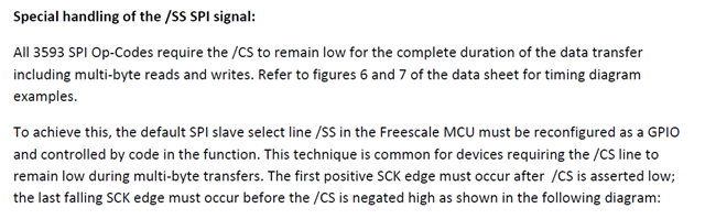
请注意,本文内容源自机器翻译,可能存在语法或其它翻译错误,仅供参考。如需获取准确内容,请参阅链接中的英语原文或自行翻译。
器件型号:TMS320F28377D 主题中讨论的其他器件:C2000WARE
我将尝试复制 HI-3593应用手册中给出的 SPI 驱动器。
ap-southeast-1-02900067-inspect.menlosecurity.com/.../
为不同的控制器(MC9S12XD)编写了驱动程序示例
我正在尝试复制两个函数 R_Register ()和 W_CommandValue ():
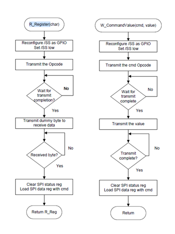
以下是应用手册中针对以下两个函数的代码:
/* ------------------------------------------------------------------
 / Read HI-3110 Register Read Function
 / ------------------------------------------------------------------
 Argument(s): Register to read
 Return: 8-bit Register Value
 */
unsigned char R_Register(char Reg)
{
    unsigned char R_Reg;
    SPI0CR1 = SPI0CR1 & ~SPI0CR1_SSOE_MASK; // disable auto /SS output, reset /SS Output Enable
    SPI0CR2 = SPI0CR2 & ~SPI0CR2_MODFEN_MASK; // disable auto /SS output, reset SPI0 Mode Fault
    SPI0_nSS = 0; // assert the SPI0 /SS strobe
    R_Reg = txrx8bits(Reg, 1); // send op code (ignore returned data byte)
    R_Reg = txrx8bits(0x00, 1); // send dummy data / receive Status Reg byte
    SPI0_nSS = 1; // negate the SPI0 /SS strobe
    SPI0CR1 = SPI0CR1 | SPI0CR1_SSOE_MASK; // enable auto /SS output, set /SS Output Enable
    SPI0CR2 = SPI0CR2 | SPI0CR2_MODFEN_MASK; // enable auto /SS output, set SPI0 Mode Fault
    return R_Reg;
}

// Write SPI Command with a Value to HI-3593
void W_CommandValue(uint8 cmd, uint8 value)
{
    uint8 dummy;
    SPI0CR1 = SPI0CR1 & ~SPI0CR1_SSOE_MASK; // disable auto /SS output, reset /SS Output
    SPI0CR2 = SPI0CR2 & ~SPI0CR2_MODFEN_MASK; // disable auto /SS output, reset SPI0 Mode
    SPI0_nSS = 0; // assert the SPI0 /SS strobe
    dummy = SPI0SR; // clear SPI status register
    SPI0DR = cmd; // SPI command
    while (!SPI0SR_SPIF)
        ;
    dummy = SPI0DR; // read Rx data in Data Reg to reset SPIF
    dummy = SPI0SR; // clear SPI status register
    SPI0DR = value; // Reset values
    while (!SPI0SR_SPIF)
        ;
    dummy = SPI0DR; // read Rx data in Data Reg to reset SPIF
    SPI0_nSS = 1; // negate the SPI0 /SS strobe
    SPI0CR1 = SPI0CR1 | SPI0CR1_SSOE_MASK; // enable auto /SS output, set /SS Output Enable
    SPI0CR2 = SPI0CR2 | SPI0CR2_MODFEN_MASK; // enable auto /SS output, set SPI0 Mode Default
}
这些是我的等效函数:
void W_CommandValue(uint16_t cmd, uint16_t value)
{
    //Pull the cs pin to low.
    GPIO_writePin(SPIA_CS_PIN, 0);
    //Wait for 100 us.
    DEVICE_DELAY_US(100);
    //Read the dummy data.
    SPI_readDataNonBlocking(A429_SPI);
    //Wait for 100 us.
    DEVICE_DELAY_US(100);
    //Write the command.
    SPI_writeDataNonBlocking(A429_SPI, cmd);
    //Wait for 100 us.
    DEVICE_DELAY_US(100);
    //Read the dummy data.
    SPI_readDataNonBlocking(A429_SPI);
    //Wait for 100 us.
    DEVICE_DELAY_US(100);
    //Write the value.
    SPI_writeDataNonBlocking(A429_SPI, value);
    //wait 100 us.
    DEVICE_DELAY_US(100);
    //Read the dummy data.
    SPI_readDataNonBlocking(A429_SPI);
    //wait 100 us.
    DEVICE_DELAY_US(100);
    //Pull the cs pin to high.
    GPIO_writePin(SPIA_CS_PIN, 1);
    //wait 100 us.
    DEVICE_DELAY_US(100);
}

uint16_t R_Register(uint16_t cmd)
{
    uint16_t value = 0;
    //Pull the cs pin to low.
    GPIO_writePin(SPIA_CS_PIN, 0);
    //Wait for 100 us.
    DEVICE_DELAY_US(100);
    //Write the command.
    SPI_writeDataNonBlocking(A429_SPI, cmd);
    //Wait for 100 us.
    DEVICE_DELAY_US(100);
    //Read the dummy byte.
    SPI_readDataNonBlocking(A429_SPI);
    //Wait for 100 us.
    DEVICE_DELAY_US(100);
    //Transmit dummy data.z
    SPI_writeDataNonBlocking(A429_SPI, 0x00);
    //Wait for 100 us.
    DEVICE_DELAY_US(100);
    //Read the received byte.
    value = SPI_readDataNonBlocking(A429_SPI);
    //Wait for 100 us.
    DEVICE_DELAY_US(100);
    //Pull the cs pin to high.
    GPIO_writePin(SPIA_CS_PIN, 1);
    return value;
}
但 无法 正常通信。
我测试了两个函数、如下所示:
void initHI3593()
{
//将上升沿赋予 HI-3593以执行硬件复位。
GPIO_writePin (A429_CA_RESET、0);
device_delay_us (100);
GPIO_writePin (A429_CA_RESET、1);
//写入 ACLK 分频寄存器(0x1400)
device_delay_us (100);
W_CommandValue (0x3800、0x1400);
device_delay_us (100);
testVar = R_Register (0xD400);
}
testVar 的值应该是0x14、但是得到的值是0x00。
有任何关于什么问题的疑虑吗?