请注意,本文内容源自机器翻译,可能存在语法或其它翻译错误,仅供参考。如需获取准确内容,请参阅链接中的英语原文或自行翻译。
器件型号:TMS320F28035 在基于 TMS320F28035的项目中、我将尝试在片上闪存中模拟 EEPROM。 我遵循了应用手册- 应用报告
《用于第2代 C2000实时 MCU 的 EEPROM 仿真》(SPRab69a1)。 我修改了以下 文件以与我的代码集成
DSP280x_Memcopy.c
F280xx_EEPROM.c
F280xx_EEPROM.h
F28035.cmd
我正在使用扇区 H ( FLASHH : origin = 0x3E8000, length = 0x002000 )
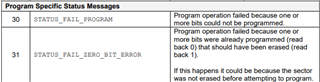
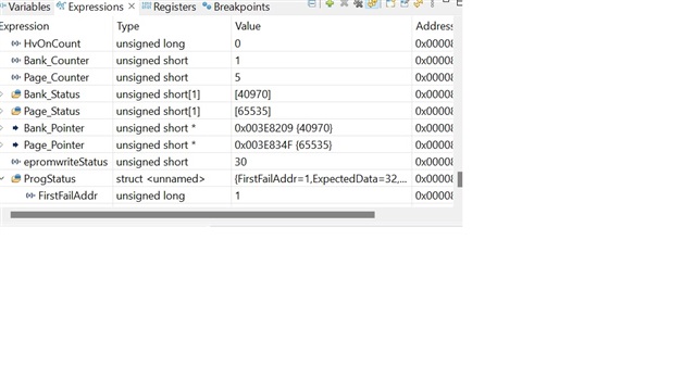
在运行代码时、EEPROM 写入操作前3到6次、然后在状态代码为30或31时失败、此外代码也会崩溃和控制器复位。
附加文件。 如果您能帮助我找到崩溃的原因、请表示感谢。
此致、
Rameshe2e.ti.com/.../0636.F280xx_5F00_EEPROM.ce2e.ti.com/.../4341.F280xx_5F00_EEPROM.he2e.ti.com/.../DSP280x_5F00_MemCopy.c
*
// TI File $Revision: /main/4 $
// Checkin $Date: November 9, 2009   15:09:12 $
//###########################################################################
//
// FILE:	F2808.cmd
//
// TITLE:	Linker Command File For F2808 Device
//
//###########################################################################
// $TI Release: F2803x Support Library v2.01.00.00 $
// $Release Date: Sun Sep 29 07:32:51 CDT 2019 $
// $Copyright:
// Copyright (C) 2009-2019 Texas Instruments Incorporated - http://www.ti.com/
//
// Redistribution and use in source and binary forms, with or without
// modification, are permitted provided that the following conditions
// are met:
//
//   Redistributions of source code must retain the above copyright
//   notice, this list of conditions and the following disclaimer.
//
//   Redistributions in binary form must reproduce the above copyright
//   notice, this list of conditions and the following disclaimer in the
//   documentation and/or other materials provided with the
//   distribution.
//
//   Neither the name of Texas Instruments Incorporated nor the names of
//   its contributors may be used to endorse or promote products derived
//   from this software without specific prior written permission.
//
// THIS SOFTWARE IS PROVIDED BY THE COPYRIGHT HOLDERS AND CONTRIBUTORS
// "AS IS" AND ANY EXPRESS OR IMPLIED WARRANTIES, INCLUDING, BUT NOT
// LIMITED TO, THE IMPLIED WARRANTIES OF MERCHANTABILITY AND FITNESS FOR
// A PARTICULAR PURPOSE ARE DISCLAIMED. IN NO EVENT SHALL THE COPYRIGHT
// OWNER OR CONTRIBUTORS BE LIABLE FOR ANY DIRECT, INDIRECT, INCIDENTAL,
// SPECIAL, EXEMPLARY, OR CONSEQUENTIAL DAMAGES (INCLUDING, BUT NOT
// LIMITED TO, PROCUREMENT OF SUBSTITUTE GOODS OR SERVICES; LOSS OF USE,
// DATA, OR PROFITS; OR BUSINESS INTERRUPTION) HOWEVER CAUSED AND ON ANY
// THEORY OF LIABILITY, WHETHER IN CONTRACT, STRICT LIABILITY, OR TORT
// (INCLUDING NEGLIGENCE OR OTHERWISE) ARISING IN ANY WAY OUT OF THE USE
// OF THIS SOFTWARE, EVEN IF ADVISED OF THE POSSIBILITY OF SUCH DAMAGE.
// $
//###########################################################################
*/

/* ======================================================
// For Code Composer Studio V2.2 and later
// ---------------------------------------
// In addition to this memory linker command file,
// add the header linker command file directly to the project.
// The header linker command file is required to link the
// peripheral structures to the proper locations within
// the memory map.
//
// The header linker files are found in <base>\DSP2803x_Headers\cmd
//
// For BIOS applications add:      DSP2803x_Headers_BIOS.cmd
// For nonBIOS applications add:   DSP2803x_Headers_nonBIOS.cmd
========================================================= */

/* ======================================================
// For Code Composer Studio prior to V2.2
// --------------------------------------
// 1) Use one of the following -l statements to include the
// header linker command file in the project. The header linker
// file is required to link the peripheral structures to the proper
// locations within the memory map                                    */

/* Uncomment this line to include file only for non-BIOS applications */
/* -l DSP2803x_Headers_nonBIOS.cmd */

/* Uncomment this line to include file only for BIOS applications */
/* -l DSP2803x_Headers_BIOS.cmd */

/* 2) In your project add the path to <base>\DSP2803x_headers\cmd to the
   library search path under project->build options, linker tab,
   library search path (-i).
/*========================================================= */

/* Define the memory block start/length for the F28035
   PAGE 0 will be used to organize program sections
   PAGE 1 will be used to organize data sections

   Notes:
         Memory blocks on F2803x are uniform (ie same
         physical memory) in both PAGE 0 and PAGE 1.
         That is the same memory region should not be
         defined for both PAGE 0 and PAGE 1.
         Doing so will result in corruption of program
         and/or data.

         L0 memory block is mirrored - that is
         it can be accessed in high memory or low memory.
         For simplicity only one instance is used in this
         linker file.

         Contiguous SARAM memory blocks or flash sectors can be
         be combined if required to create a larger memory block.
*/

MEMORY
{
PAGE 0:    /* Program Memory */
           /* Memory (RAM/FLASH/OTP) blocks can be moved to PAGE1 for data allocation */
   RAML0       : origin = 0x008000, length = 0x000800     /* on-chip RAM block L0 */
   RAML1       : origin = 0x008800, length = 0x000400     /* on-chip RAM block L1 */
   OTP         : origin = 0x3D7800, length = 0x000400     /* on-chip OTP */
   FLASHH      : origin = 0x3E8000, length = 0x002000     /* on-chip FLASH */
   FLASHG      : origin = 0x3EA000, length = 0x002000     /* on-chip FLASH */
   FLASHF      : origin = 0x3EC000, length = 0x002000     /* on-chip FLASH */
   FLASHE      : origin = 0x3EE000, length = 0x002000     /* on-chip FLASH */
   FLASHD      : origin = 0x3F0000, length = 0x002000     /* on-chip FLASH */
   FLASHC      : origin = 0x3F2000, length = 0x002000     /* on-chip FLASH */
   FLASHA      : origin = 0x3F6000, length = 0x001F80     /* on-chip FLASH */
   CSM_RSVD    : origin = 0x3F7F80, length = 0x000076     /* Part of FLASHA.  Program with all 0x0000 when CSM is in use. */
   BEGIN       : origin = 0x3F7FF6, length = 0x000002     /* Part of FLASHA.  Used for "boot to Flash" bootloader mode. */
   CSM_PWL_P0  : origin = 0x3F7FF8, length = 0x000008     /* Part of FLASHA.  CSM password locations in FLASHA */

   IQTABLES    : origin = 0x3FE000, length = 0x000B50     /* IQ Math Tables in Boot ROM */
   IQTABLES2   : origin = 0x3FEB50, length = 0x00008C     /* IQ Math Tables in Boot ROM */
   IQTABLES3   : origin = 0x3FEBDC, length = 0x0000AA	  /* IQ Math Tables in Boot ROM */

   ROM         : origin = 0x3FF27C, length = 0x000D44     /* Boot ROM */
   RESET       : origin = 0x3FFFC0, length = 0x000002     /* part of boot ROM  */
   VECTORS     : origin = 0x3FFFC2, length = 0x00003E     /* part of boot ROM  */

PAGE 1 :   /* Data Memory */
           /* Memory (RAM/FLASH/OTP) blocks can be moved to PAGE0 for program allocation */
           /* Registers remain on PAGE1                                                  */
   BOOT_RSVD   : origin = 0x000000, length = 0x000050     /* Part of M0, BOOT rom will use this for stack */
   RAMM0       : origin = 0x000050, length = 0x0003B0     /* on-chip RAM block M0 */
   RAMM1       : origin = 0x000400, length = 0x000400     /* on-chip RAM block M1 */
   RAML2       : origin = 0x008C00, length = 0x000400     /* on-chip RAM block L2 */
   RAML3       : origin = 0x009000, length = 0x001000     /* on-chip RAM block L3 */
   FLASHB      : origin = 0x3F4000, length = 0x002000     /* on-chip FLASH */

}

/* Allocate sections to memory blocks.
   Note:
         codestart user defined section in DSP28_CodeStartBranch.asm used to redirect code
                   execution when booting to flash
         ramfuncs  user defined section to store functions that will be copied from Flash into RAM
*/

SECTIONS
{

   /* Allocate program areas: */
   .cinit              : > FLASHA      PAGE = 0
   .pinit              : > FLASHA,     PAGE = 0
 /*  .text               : > FLASHA      PAGE = 0 */
   .text             : >> FLASHD | FLASHC | FLASHA,     PAGE = 0
   codestart           : > BEGIN       PAGE = 0
       Flash28_API:
   {
        -lFlash2803x_API_V100.lib(.econst)
        -lFlash2803x_API_V100.lib(.text)
   }                   LOAD = FLASHA,
                       RUN = RAML0,
                       LOAD_START(_Flash28_API_LoadStart),
                       LOAD_END(_Flash28_API_LoadEnd),
                       RUN_START(_Flash28_API_RunStart),
                       PAGE = 0

   ramfuncs            : LOAD = FLASHD,
                         RUN = RAML0,
                         LOAD_START(_RamfuncsLoadStart),
                         LOAD_END(_RamfuncsLoadEnd),
                         RUN_START(_RamfuncsRunStart),
                         PAGE = 0

   csmpasswds          : > CSM_PWL_P0  PAGE = 0
   csm_rsvd            : > CSM_RSVD    PAGE = 0

   /* Allocate uninitalized data sections: */
 /* .stack              : > RAMM1    PAGE = 1 */  /* change this to Raml3 */
    .stack              : > RAML3    PAGE = 1
 /*     .stack              : >> RAMM1 | RAMM0,   PAGE = 1 8/
 /*     .stack              : > RAMM0       PAGE = 1  */
   .ebss               : > RAML2       PAGE = 1
   .esysmem            : > RAML2       PAGE = 1

   /* Initalized sections go in Flash */
   /* For SDFlash to program these, they must be allocated to page 0 */
   .econst             : > FLASHA      PAGE = 0
   .switch             : > FLASHA      PAGE = 0

   /* Allocate IQ math areas: */
   IQmath              : > FLASHA      PAGE = 0            /* Math Code */
   IQmathTables        : > IQTABLES,   PAGE = 0, TYPE = NOLOAD

  /* Uncomment the section below if calling the IQNexp() or IQexp()
      functions from the IQMath.lib library in order to utilize the
      relevant IQ Math table in Boot ROM (This saves space and Boot ROM
      is 1 wait-state). If this section is not uncommented, IQmathTables2
      will be loaded into other memory (SARAM, Flash, etc.) and will take
      up space, but 0 wait-state is possible.
   */
   /*
   IQmathTables2    : > IQTABLES2, PAGE = 0, TYPE = NOLOAD
   {

              IQmath.lib<IQNexpTable.obj> (IQmathTablesRam)

   }
   */
    /* Uncomment the section below if calling the IQNasin() or IQasin()
       functions from the IQMath.lib library in order to utilize the
       relevant IQ Math table in Boot ROM (This saves space and Boot ROM
       is 1 wait-state). If this section is not uncommented, IQmathTables2
       will be loaded into other memory (SARAM, Flash, etc.) and will take
       up space, but 0 wait-state is possible.
    */
    /*
    IQmathTables3    : > IQTABLES3, PAGE = 0, TYPE = NOLOAD
    {

               IQmath.lib<IQNasinTable.obj> (IQmathTablesRam)

    }
    */

   /* .reset is a standard section used by the compiler.  It contains the */
   /* the address of the start of _c_int00 for C Code.   /*
   /* When using the boot ROM this section and the CPU vector */
   /* table is not needed.  Thus the default type is set here to  */
   /* DSECT  */
   .reset              : > RESET,      PAGE = 0, TYPE = DSECT
   vectors             : > VECTORS     PAGE = 0, TYPE = DSECT

}

/*
//===========================================================================
// End of file.
//===========================================================================
*/