请注意,本文内容源自机器翻译,可能存在语法或其它翻译错误,仅供参考。如需获取准确内容,请参阅链接中的英语原文或自行翻译。
器件型号:TMS320F2800137 主题中讨论的其他器件:C2000WARE、 SysConfig、
e2e.ti.com/.../2023_2D00_10_2D00_05-12_2D00_18_2D00_19.mp4
请尽快解决问题。

This thread has been locked.
If you have a related question, please click the "Ask a related question" button in the top right corner. The newly created question will be automatically linked to this question.
e2e.ti.com/.../2023_2D00_10_2D00_05-12_2D00_18_2D00_19.mp4
请尽快解决问题。
尊敬的所有人:
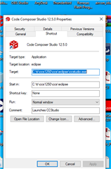
我们安装了最新的 CCS 版本:Code Composer Studio 12.5.0
您在尝试导入其他实验(例如本实验的 controlCARD 版本或其他 F280013x 培训实验)时是否遇到相同的问题? 还是只有这个 ADC 培训实验会给您带来问题?
对于所有具有相同问题的问题、请尽早解决、因为我们的项目因上次 week.e2e.ti.com/.../2023_2D00_10_2D00_06-10_2D00_57_2D00_56.mp4中的此问题而出现延迟
您好!
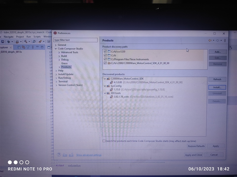
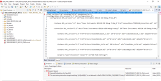
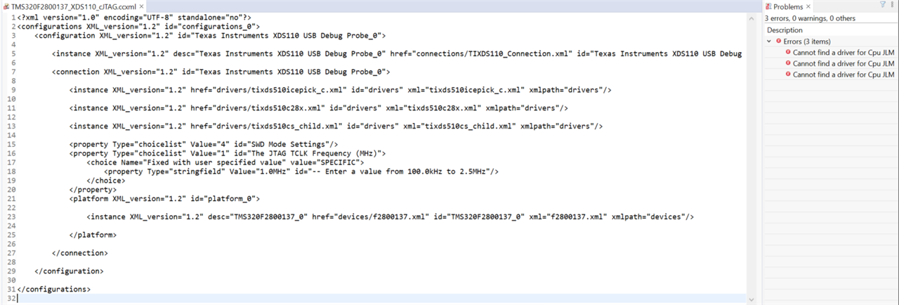
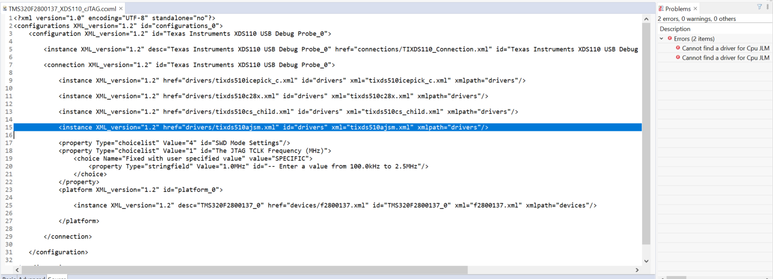
CCS 需要将 C2000Ware 检测为产品。 您可以通过依次单击"CCS"->"Windows"->"Preferences"->"Products"
此时会打开一个列出所有产品的窗口、请参阅以下快照
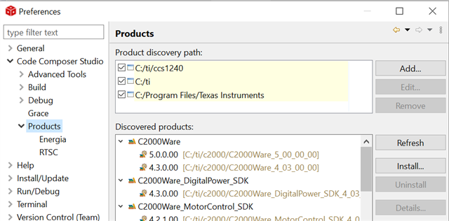
如果 C2000Ware 未列出、请尝试通过此链接 https://www.ti.com/tool/download/C2000WARE 安装 C2000Ware。
然后导入项目。
此致
西达尔特
由于未列出 C2000Ware、因此请尝试通过此链接 https://www.ti.com/tool/download/C2000WARE 安装 C2000Ware 、然后导入工程。
此致
西达尔特
//#############################################################################
//
// FILE: lab_main.c
//
// TITLE: adc lab
//
// C2K ACADEMY URL: dev.ti.com/.../node
//
//! \addtogroup academy_lab_list
//! <h1> Using Analog Subsystems Lab - Sysconfig </h1>
//!
//! The objective of this lab exercise is to become familiar with the
//! programming and operation of the on-chip analog-to-digital converter (ADC).
//! The microcontroller (MCU) will be setup to sample a single ADC input
//! channel at a prescribed sampling rate and store the conversion result in a
//! circular memory buffer. In the second part of this lab exercise, the
//! digital-to-analog converter (DAC) will be explored.
//!
//! \b External \b Connections \n
//!  - Refer to Academy Lab instruction for exact pin for your device/board
//!
//! \b Watch \b Variables \n
//!  - None.
//!
//#############################################################################
// $Copyright:
// Copyright (C) 2022 Texas Instruments Incorporated - http://www.ti.com
//
// Redistribution and use in source and binary forms, with or without
// modification, are permitted provided that the following conditions
// are met:
//
//   Redistributions of source code must retain the above copyright
//   notice, this list of conditions and the following disclaimer.
//
//   Redistributions in binary form must reproduce the above copyright
//   notice, this list of conditions and the following disclaimer in the
//   documentation and/or other materials provided with the
//   distribution.
//
//   Neither the name of Texas Instruments Incorporated nor the names of
//   its contributors may be used to endorse or promote products derived
//   from this software without specific prior written permission.
//
// THIS SOFTWARE IS PROVIDED BY THE COPYRIGHT HOLDERS AND CONTRIBUTORS
// "AS IS" AND ANY EXPRESS OR IMPLIED WARRANTIES, INCLUDING, BUT NOT
// LIMITED TO, THE IMPLIED WARRANTIES OF MERCHANTABILITY AND FITNESS FOR
// A PARTICULAR PURPOSE ARE DISCLAIMED. IN NO EVENT SHALL THE COPYRIGHT
// OWNER OR CONTRIBUTORS BE LIABLE FOR ANY DIRECT, INDIRECT, INCIDENTAL,
// SPECIAL, EXEMPLARY, OR CONSEQUENTIAL DAMAGES (INCLUDING, BUT NOT
// LIMITED TO, PROCUREMENT OF SUBSTITUTE GOODS OR SERVICES; LOSS OF USE,
// DATA, OR PROFITS; OR BUSINESS INTERRUPTION) HOWEVER CAUSED AND ON ANY
// THEORY OF LIABILITY, WHETHER IN CONTRACT, STRICT LIABILITY, OR TORT
// (INCLUDING NEGLIGENCE OR OTHERWISE) ARISING IN ANY WAY OUT OF THE USE
// OF THIS SOFTWARE, EVEN IF ADVISED OF THE POSSIBILITY OF SUCH DAMAGE.
// $
//#############################################################################


//
// Included Files
//
#include "board.h"

//
// Global variables and definitions
//
#define ADC_BUF_LEN         50
uint16_t DEBUG_TOGGLE = 1;    // Used for real-time mode
uint16_t AdcBuf[ADC_BUF_LEN];  // ADC buffer allocation

#ifdef DACB_BASE
uint16_t DacOutput;
uint16_t DacOffset;
uint16_t SINE_ENABLE = 0;

// quadrature look-up table: contains 4 quadrants of sinusoid data points
#define SINE_PTS 25
int QuadratureTable[SINE_PTS] = {
        0x0000,         // [0]  0.0
        0x1FD4,         // [1]  14.4
        0x3DA9,         // [2]  28.8
        0x579E,         // [3]  43.2
        0x6C12,         // [4]  57.6
        0x79BB,         // [5]  72.0
        0x7FBE,         // [6]  86.4
        0x7DBA,         // [7]  100.8
        0x73D0,         // [8]  115.2
        0x629F,         // [9]  129.6
        0x4B3B,         // [10] 144.0
        0x2F1E,         // [11] 158.4
        0x100A,         // [12] 172.8
        0xEFF6,         // [13] 187.2
        0xD0E2,         // [14] 201.6
        0xB4C5,         // [15] 216.0
        0x9D61,         // [16] 230.4
        0x8C30,         // [17] 244.8
        0x8246,         // [18] 259.2
        0x8042,         // [19] 273.6
        0x8645,         // [20] 288.0
        0x93EE,         // [21] 302.4
        0xA862,         // [22] 316.8
        0xC257,         // [23] 331.2
        0xE02C          // [24] 345.6
        };
#endif

//
// Function Declarations
//
__interrupt void INT_myADCA_1_ISR(void);

//
// Main
//
void main(void)
{
    // CPU Initialization
    Device_init();
    Interrupt_initModule();
    Interrupt_initVectorTable();

    // Configure the GPIOs/ADC/PWM through SysConfig generated files
    Board_init();

    // Enable global interrupts and real-time debug
    EINT;
    ERTM;

    // Main Loop
    while(1){}

}

interrupt void INT_myADCA_1_ISR(void)
{
    static uint16_t *AdcBufPtr = AdcBuf;
    uint16_t LED_count = 0;

    // Read the ADC Result
    *AdcBufPtr++ = ADC_readResult(myADCA_RESULT_BASE, myADCA_SOC0);

    // Brute Force the circular buffer
    if (AdcBufPtr == (AdcBuf + ADC_BUF_LEN))
    {
        AdcBufPtr = AdcBuf;
    }

    // Toggle the pin
    if(DEBUG_TOGGLE == 1)
    {
        GPIO_togglePin(myGPIOToggle);
    }

    if(LED_count++ > 25000)                      // Toggle slowly to see the LED blink
    {
        GPIO_togglePin(myBoardLED0_GPIO);                   // Toggle the pin
        LED_count = 0;                           // Reset the counter
    }

#ifdef DACB_BASE
    // Write to DAC-B to create input to ADC-A0
    static uint16_t iQuadratureTable = 0;        // Quadrature table index

    if(SINE_ENABLE == 1)
    {
        DacOutput = DacOffset + ((QuadratureTable[iQuadratureTable++] ^ 0x8000) >> 5);
    }
    else
    {
        DacOutput = DacOffset;
    }
    if(iQuadratureTable > (SINE_PTS - 1))        // Wrap the index
    {
        iQuadratureTable = 0;
    }
    DAC_setShadowValue(myDACB_BASE, DacOutput);
#endif

    Interrupt_clearACKGroup(INT_myADCA_1_INTERRUPT_ACK_GROUP);
    ADC_clearInterruptStatus(myADCA_BASE, ADC_INT_NUMBER1);
} // End of ADC ISR
//
// End of File
//
//#############################################################################
//
// FILE:   device.h
//
// TITLE:  Device setup for examples.
//
//#############################################################################
//
//
// $Copyright:
// Copyright (C) 2023 Texas Instruments Incorporated - http://www.ti.com/
//
// Redistribution and use in source and binary forms, with or without
// modification, are permitted provided that the following conditions
// are met:
//
//   Redistributions of source code must retain the above copyright
//   notice, this list of conditions and the following disclaimer.
//
//   Redistributions in binary form must reproduce the above copyright
//   notice, this list of conditions and the following disclaimer in the
//   documentation and/or other materials provided with the
//   distribution.
//
//   Neither the name of Texas Instruments Incorporated nor the names of
//   its contributors may be used to endorse or promote products derived
//   from this software without specific prior written permission.
//
// THIS SOFTWARE IS PROVIDED BY THE COPYRIGHT HOLDERS AND CONTRIBUTORS
// "AS IS" AND ANY EXPRESS OR IMPLIED WARRANTIES, INCLUDING, BUT NOT
// LIMITED TO, THE IMPLIED WARRANTIES OF MERCHANTABILITY AND FITNESS FOR
// A PARTICULAR PURPOSE ARE DISCLAIMED. IN NO EVENT SHALL THE COPYRIGHT
// OWNER OR CONTRIBUTORS BE LIABLE FOR ANY DIRECT, INDIRECT, INCIDENTAL,
// SPECIAL, EXEMPLARY, OR CONSEQUENTIAL DAMAGES (INCLUDING, BUT NOT
// LIMITED TO, PROCUREMENT OF SUBSTITUTE GOODS OR SERVICES; LOSS OF USE,
// DATA, OR PROFITS; OR BUSINESS INTERRUPTION) HOWEVER CAUSED AND ON ANY
// THEORY OF LIABILITY, WHETHER IN CONTRACT, STRICT LIABILITY, OR TORT
// (INCLUDING NEGLIGENCE OR OTHERWISE) ARISING IN ANY WAY OUT OF THE USE
// OF THIS SOFTWARE, EVEN IF ADVISED OF THE POSSIBILITY OF SUCH DAMAGE.
// $
//#############################################################################

#ifndef __DEVICE_H__
#define __DEVICE_H__

#ifdef __cplusplus
extern "C"
{
#endif

//
// Included Files
//
#include "driverlib.h"

//
// Check for invalid compile flags
//
#if defined(__TMS320C28XX_FPU64__)
#error "Invalid FPU Configuration"
#endif
#if defined(__TMS320C28XX_TMU1__)
#error "Invalid TMU Configuration"
#endif

//*****************************************************************************
//
// Defines for pin numbers
//
//*****************************************************************************
#ifdef _LAUNCHXL_F2800137
//
// LaunchPad
//
//
// LEDs
//
#define DEVICE_GPIO_PIN_LED1        20U             // GPIO number for LED4
#define DEVICE_GPIO_PIN_LED2        22U             // GPIO number for LED5
#define DEVICE_GPIO_CFG_LED1        GPIO_20_GPIO20  // "pinConfig" for LED4
#define DEVICE_GPIO_CFG_LED2        GPIO_22_GPIO22  // "pinConfig" for LED5

//
// CANA
//
#define DEVICE_GPIO_PIN_CANRXA      5U              // GPIO number for CANA RX
#define DEVICE_GPIO_PIN_CANTXA      4U              // GPIO number for CANA TX
#define DEVICE_GPIO_CFG_CANRXA      GPIO_5_CANA_RX  // "pinConfig" for CANA RX
#define DEVICE_GPIO_CFG_CANTXA      GPIO_4_CANA_TX  // "pinConfig" for CANA TX

//
// SCI for USB-to-UART adapter on XDS110 chip
//
#define DEVICE_GPIO_PIN_SCIRXDA     28U             // GPIO number for SCIA RX
#define DEVICE_GPIO_PIN_SCITXDA     29U             // GPIO number for SCIA TX
#define DEVICE_GPIO_CFG_SCIRXDA     GPIO_28_SCIA_RX // "pinConfig" for SCIA RX
#define DEVICE_GPIO_CFG_SCITXDA     GPIO_29_SCIA_TX // "pinConfig" for SCIA TX

//
// I2CA
//
#define DEVICE_GPIO_PIN_SDAA        32U  // GPIO number for I2C SDAA
#define DEVICE_GPIO_PIN_SCLA        33U  // GPIO number for I2C SCLA
#define DEVICE_GPIO_CFG_SDAA        GPIO_32_I2CA_SDA  // "pinConfig" for I2C SDAA
#define DEVICE_GPIO_CFG_SCLA        GPIO_33_I2CA_SCL  // "pinConfig" for I2C SCLA

#define DEVICE_GPIO_PIN_SDAA_2      19U  // GPIO number for I2C SDAA
#define DEVICE_GPIO_PIN_SCLA_2      18U  // GPIO number for I2C SCLA
#define DEVICE_GPIO_CFG_SDAA_2      GPIO_19_I2CA_SDA  // "pinConfig" for I2C SDAA
#define DEVICE_GPIO_CFG_SCLA_2      GPIO_18_I2CA_SCL  // "pinConfig" for I2C SCLA

#define DEVICE_GPIO_PIN_SDAB        28U  // GPIO number for I2C SDAA
#define DEVICE_GPIO_PIN_SCLB        29U  // GPIO number for I2C SCLA
#define DEVICE_GPIO_CFG_SDAB        GPIO_28_I2CB_SDA  // "pinConfig" for I2C SDAA
#define DEVICE_GPIO_CFG_SCLB        GPIO_29_I2CB_SCL  // "pinConfig" for I2C SCLA

//
// SPIA
//
#define DEVICE_GPIO_PIN_SPICLKA     9U   // GPIO number for SPI CLKA
#define DEVICE_GPIO_PIN_SPISIMOA    8U   // GPIO number for SPI SIMOA
#define DEVICE_GPIO_PIN_SPISOMIA    17U  // GPIO number for SPI SOMIA
#define DEVICE_GPIO_PIN_SPISTEA     5U   // GPIO number for SPI STEA
#define DEVICE_GPIO_CFG_SPICLKA     GPIO_9_SPIA_CLK    // "pinConfig" for SPI CLKA
#define DEVICE_GPIO_CFG_SPISIMOA    GPIO_8_SPIA_SIMO   // "pinConfig" for SPI SIMOA
#define DEVICE_GPIO_CFG_SPISOMIA    GPIO_17_SPIA_SOMI  // "pinConfig" for SPI SOMIA
#define DEVICE_GPIO_CFG_SPISTEA     GPIO_5_SPIA_STE    // "pinConfig" for SPI STEA

//
// eQEP1
//
#define DEVICE_GPIO_PIN_EQEP1A      40U  // GPIO number for EQEP 1A
#define DEVICE_GPIO_PIN_EQEP1B      41U  // GPIO number for EQEP 1B
#define DEVICE_GPIO_PIN_EQEP1I      39U  // GPIO number for EQEP 1I
#define DEVICE_GPIO_CFG_EQEP1A      GPIO_40_EQEP1_A  // "pinConfig" for EQEP 1A
#define DEVICE_GPIO_CFG_EQEP1B      GPIO_41_EQEP1_B  // "pinConfig" for EQEP 1B
#define DEVICE_GPIO_CFG_EQEP1I      GPIO_39_EQEP1_INDEX  // "pinConfig" for EQEP 1I

#else
//
// ControlCARD
//

//
// LEDs
//
#define DEVICE_GPIO_PIN_LED1        24U             // GPIO number for LED1
#define DEVICE_GPIO_PIN_LED2        39U             // GPIO number for LED2
#define DEVICE_GPIO_CFG_LED1        GPIO_24_GPIO24  // "pinConfig" for LED1
#define DEVICE_GPIO_CFG_LED2        GPIO_39_GPIO39  // "pinConfig" for LED2

//
// CANA
//
#define DEVICE_GPIO_PIN_CANTXA      32U              // GPIO number for CANTXA
#define DEVICE_GPIO_PIN_CANRXA      33U              // GPIO number for CANRXA
#define DEVICE_GPIO_CFG_CANRXA      GPIO_33_CANA_RX  // "pinConfig" for CANA RX
#define DEVICE_GPIO_CFG_CANTXA      GPIO_32_CANA_TX  // "pinConfig" for CANA TX

//
// SCI for USB-to-UART adapter on FTDI chip
//
#define DEVICE_GPIO_PIN_SCIRXDA     28U             // GPIO number for SCI RX
#define DEVICE_GPIO_PIN_SCITXDA     29U             // GPIO number for SCI TX
#define DEVICE_GPIO_CFG_SCIRXDA     GPIO_28_SCIA_RX // "pinConfig" for SCI RX
#define DEVICE_GPIO_CFG_SCITXDA     GPIO_29_SCIA_TX // "pinConfig" for SCI TX

//
// I2C
//
#define DEVICE_GPIO_PIN_SDAA        32U  // GPIO number for I2C SDAA
#define DEVICE_GPIO_PIN_SCLA        33U  // GPIO number for I2C SCLA
#define DEVICE_GPIO_CFG_SDAA        GPIO_32_I2CA_SDA  // "pinConfig" for I2C SDAA
#define DEVICE_GPIO_CFG_SCLA        GPIO_33_I2CA_SCL  // "pinConfig" for I2C SCLA

//I2CB GPIO pins
#define DEVICE_GPIO_PIN_SDAB    2
#define DEVICE_GPIO_PIN_SCLB    3

#define DEVICE_GPIO_CFG_SDAB GPIO_2_I2CB_SDA
#define DEVICE_GPIO_CFG_SCLB GPIO_3_I2CB_SCL

#endif

//*****************************************************************************
//
// Defines related to clock configuration
//
//*****************************************************************************

//
// To use XTAL as the clock source, uncomment #define USE_PLL_SRC_XTAL,
// and comment the #define USE_PLL_SRC_INTOSC
//
//#define USE_PLL_SRC_XTAL
#define USE_PLL_SRC_INTOSC

//
// To use CPU frequency as 100MHZ, uncomment #define CPU_FRQ_100MHZ,
// and comment the #define CPU_FRQ_120MHZ
//
//#define CPU_FRQ_100MHZ
#define CPU_FRQ_120MHZ

#if defined(USE_PLL_SRC_XTAL)
//
// 20MHz XTAL on controlCARD is used as the PLL source.
// For use with SysCtl_getClock().
//
#define DEVICE_OSCSRC_FREQ          20000000U


#if defined(CPU_FRQ_100MHZ)

//
// Define to pass to SysCtl_setClock(). Will configure the clock as follows:
// PLLSYSCLK = 20MHz (XTAL_OSC) * 30 (IMULT) / (2 (REFDIV) * 3 (ODIV) * 1(SYSDIV))
//
#define DEVICE_SETCLOCK_CFG          (SYSCTL_OSCSRC_XTAL | SYSCTL_IMULT(30) | \
                                      SYSCTL_REFDIV(2) | SYSCTL_ODIV(3) | \
                                      SYSCTL_SYSDIV(1) | SYSCTL_PLL_ENABLE | \
                                      SYSCTL_DCC_BASE_0)

//
// 100MHz SYSCLK frequency based on the above DEVICE_SETCLOCK_CFG. Update the
// code below if a different clock configuration is used!
//
#define DEVICE_SYSCLK_FREQ          ((DEVICE_OSCSRC_FREQ * 30) / (2 * 3 * 1))
#elif defined(CPU_FRQ_120MHZ)

//
// Define to pass to SysCtl_setClock(). Will configure the clock as follows:
// PLLSYSCLK = 20MHz (XTAL_OSC) * 48 (IMULT) / (2 (REFDIV) * 4 (ODIV) * 1(SYSDIV))
//
#define DEVICE_SETCLOCK_CFG          (SYSCTL_OSCSRC_XTAL | SYSCTL_IMULT(48) | \
                                      SYSCTL_REFDIV(2) | SYSCTL_ODIV(4) | \
                                      SYSCTL_SYSDIV(1) | SYSCTL_PLL_ENABLE | \
                                      SYSCTL_DCC_BASE_0)

//
// 120MHz SYSCLK frequency based on the above DEVICE_SETCLOCK_CFG. Update the
// code below if a different clock configuration is used!
//
#define DEVICE_SYSCLK_FREQ          ((DEVICE_OSCSRC_FREQ * 48) / (2 * 4 * 1))
#endif
#elif defined(USE_PLL_SRC_INTOSC)
//
// 10MHz INTOSC on the device is used as the PLL source.
// For use with SysCtl_getClock().
//
#define DEVICE_OSCSRC_FREQ          10000000U
#if defined(CPU_FRQ_100MHZ)
//
// Define to pass to SysCtl_setClock(). Will configure the clock as follows:
// PLLSYSCLK = 10MHz (INT_OSC2) * 30 (IMULT) / (1 (REFDIV) * 3 (ODIV) * 1(SYSDIV))
//
#define DEVICE_SETCLOCK_CFG          (SYSCTL_OSCSRC_OSC2 | SYSCTL_IMULT(30) | \
                                      SYSCTL_REFDIV(1) | SYSCTL_ODIV(3) | \
                                      SYSCTL_SYSDIV(1) | SYSCTL_PLL_ENABLE | \
                                      SYSCTL_DCC_BASE_0)

//
// 100MHz SYSCLK frequency based on the above DEVICE_SETCLOCK_CFG. Update the
// code below if a different clock configuration is used!
//
#define DEVICE_SYSCLK_FREQ          ((DEVICE_OSCSRC_FREQ * 30) / (1 * 3 * 1))
#elif defined(CPU_FRQ_120MHZ)
//
// Define to pass to SysCtl_setClock(). Will configure the clock as follows:
// PLLSYSCLK = 10MHz (INT_OSC2) * 48 (IMULT) / (1 (REFDIV) * 4 (ODIV) * 1(SYSDIV))
//
#define DEVICE_SETCLOCK_CFG          (SYSCTL_OSCSRC_OSC2 | SYSCTL_IMULT(48) | \
                                      SYSCTL_REFDIV(1) | SYSCTL_ODIV(4) | \
                                      SYSCTL_SYSDIV(1) | SYSCTL_PLL_ENABLE | \
                                      SYSCTL_DCC_BASE_0)

//
// 120MHz SYSCLK frequency based on the above DEVICE_SETCLOCK_CFG. Update the
// code below if a different clock configuration is used!
//
#define DEVICE_SYSCLK_FREQ          ((DEVICE_OSCSRC_FREQ * 48) / (1 * 4 * 1))
#endif
#endif

//
// 30MHz (25MHz in case if DEVICE_SYSCLK_FREQ = 100MHz) LSPCLK frequency based on the above DEVICE_SYSCLK_FREQ and a default
// low speed peripheral clock divider of 4. Update the code below if a
// different LSPCLK divider is used!
//
#define DEVICE_LSPCLK_FREQ          (DEVICE_SYSCLK_FREQ / 4)

//*****************************************************************************
//
// Macro to call SysCtl_delay() to achieve a delay in microseconds. The macro
// will convert the desired delay in microseconds to the count value expected
// by the function. \b x is the number of microseconds to delay.
//
//*****************************************************************************
#define DEVICE_DELAY_US(x) SysCtl_delay(((((long double)(x)) / (1000000.0L /  \
                              (long double)DEVICE_SYSCLK_FREQ)) - 9.0L) / 5.0L)

//*****************************************************************************
//
// Defines, Globals, and Header Includes related to Flash Support
//
//*****************************************************************************
#ifdef _FLASH
#include <stddef.h>

#ifndef CMDTOOL
extern uint16_t RamfuncsLoadStart;
extern uint16_t RamfuncsLoadEnd;
extern uint16_t RamfuncsLoadSize;
extern uint16_t RamfuncsRunStart;
extern uint16_t RamfuncsRunEnd;
extern uint16_t RamfuncsRunSize;
#endif

#endif

#define DEVICE_FLASH_WAITSTATES 2

//*****************************************************************************
//
// Function Prototypes
//
//*****************************************************************************
//*****************************************************************************
//
//! \addtogroup device_api
//! @{
//
//*****************************************************************************

//*****************************************************************************
//
//! @brief Function to initialize the device. Primarily initializes system
//!  control to aknown state by disabling the watchdog, setting up the
//!  SYSCLKOUT frequency, and enabling the clocks to the peripherals.
//!
//! \param None.
//! \return None.
//
//*****************************************************************************
extern void Device_init(void);

//*****************************************************************************
//!
//!
//! @brief Function to turn on all peripherals, enabling reads and writes to the
//! peripherals' registers.
//!
//! Note that to reduce power, unused peripherals should be disabled.
//!
//! @param None
//! @return None
//
//*****************************************************************************
extern void Device_enableAllPeripherals(void);
//*****************************************************************************
//!
//!
//! @brief Function to disable pin locks on GPIOs.
//!
//! @param None
//! @return None
//
//*****************************************************************************
extern void Device_initGPIO(void);

//*****************************************************************************
//!
//! @brief Error handling function to be called when an ASSERT is violated
//!
//! @param *filename File name in which the error has occurred
//! @param line Line number within the file
//! @return None
//
//*****************************************************************************
extern void __error__(const char *filename, uint32_t line);

//*****************************************************************************
//
// Close the Doxygen group.
//! @}
//
//*****************************************************************************

#ifdef __cplusplus
}
#endif

#endif // __DEVICE_H__
您好!
更改 SysConfig 配置不会更新 lab_main.c 或 device.h 文件。 它会生成文件 board.c 和 board.h、您可在其中查看在 SysConfig 中完成的更改。
请访问以下链接
https://software-dl.ti.com/C2000/docs/software_guide/c2000_sysconfig.html
视频- https://www.ti.com/video/6304748751001
此致
西达尔特
尊敬的 Siddharth:
请查看所附的 J17、即 TENVI 问题、为什么每次程序进入错误循环/起作用?
e2e.ti.com/.../TENVI_5F00_issue.mp4
请检查并解决此问题。
/*
 * Copyright (c) 2020 Texas Instruments Incorporated - http://www.ti.com
 * All rights reserved.
 *
 * Redistribution and use in source and binary forms, with or without
 * modification, are permitted provided that the following conditions
 * are met:
 *
 * *  Redistributions of source code must retain the above copyright
 *    notice, this list of conditions and the following disclaimer.
 *
 * *  Redistributions in binary form must reproduce the above copyright
 *    notice, this list of conditions and the following disclaimer in the
 *    documentation and/or other materials provided with the distribution.
 *
 * *  Neither the name of Texas Instruments Incorporated nor the names of
 *    its contributors may be used to endorse or promote products derived
 *    from this software without specific prior written permission.
 *
 * THIS SOFTWARE IS PROVIDED BY THE COPYRIGHT HOLDERS AND CONTRIBUTORS "AS IS"
 * AND ANY EXPRESS OR IMPLIED WARRANTIES, INCLUDING, BUT NOT LIMITED TO,
 * THE IMPLIED WARRANTIES OF MERCHANTABILITY AND FITNESS FOR A PARTICULAR
 * PURPOSE ARE DISCLAIMED. IN NO EVENT SHALL THE COPYRIGHT OWNER OR
 * CONTRIBUTORS BE LIABLE FOR ANY DIRECT, INDIRECT, INCIDENTAL, SPECIAL,
 * EXEMPLARY, OR CONSEQUENTIAL DAMAGES (INCLUDING, BUT NOT LIMITED TO,
 * PROCUREMENT OF SUBSTITUTE GOODS OR SERVICES; LOSS OF USE, DATA, OR PROFITS;
 * OR BUSINESS INTERRUPTION) HOWEVER CAUSED AND ON ANY THEORY OF LIABILITY,
 * WHETHER IN CONTRACT, STRICT LIABILITY, OR TORT (INCLUDING NEGLIGENCE OR
 * OTHERWISE) ARISING IN ANY WAY OUT OF THE USE OF THIS SOFTWARE,
 * EVEN IF ADVISED OF THE POSSIBILITY OF SUCH DAMAGE.
 *
 */

#include "board.h"

//*****************************************************************************
//
// Board Configurations
// Initializes the rest of the modules.
// Call this function in your application if you wish to do all module
// initialization.
// If you wish to not use some of the initializations, instead of the
// Board_init use the individual Module_inits
//
//*****************************************************************************
void Board_init()
{
	EALLOW;

	PinMux_init();
	SYNC_init();
	ASYSCTL_init();
	ADC_init();
	EPWM_init();
	GPIO_init();
	INTERRUPT_init();

	EDIS;
}

//*****************************************************************************
//
// PINMUX Configurations
//
//*****************************************************************************
void PinMux_init()
{
	//
	// PinMux for modules assigned to CPU1
	//

	//
	// ANALOG -> temp_ensor Pinmux
	//
	// Analog PinMux for A15/C7
	GPIO_setPinConfig(GPIO_233_GPIO233);
	// AIO -> Analog mode selected
	GPIO_setAnalogMode(233, GPIO_ANALOG_ENABLED);
	// Analog PinMux for A18/C18, GPIO21
	GPIO_setPinConfig(GPIO_21_GPIO21);
	// AGPIO -> Analog mode selected
	GPIO_setAnalogMode(21, GPIO_ANALOG_ENABLED);
	// Analog PinMux for C6, GPIO226
	GPIO_setPinConfig(GPIO_226_GPIO226);
	// AGPIO -> Analog mode selected
	GPIO_setAnalogMode(226, GPIO_ANALOG_ENABLED);
	//
	// EPWM1 -> myEPWM0 Pinmux
	//
	GPIO_setPinConfig(myEPWM0_EPWMA_PIN_CONFIG);
	GPIO_setPadConfig(myEPWM0_EPWMA_GPIO, GPIO_PIN_TYPE_STD);
	GPIO_setQualificationMode(myEPWM0_EPWMA_GPIO, GPIO_QUAL_SYNC);

	GPIO_setPinConfig(myEPWM0_EPWMB_PIN_CONFIG);
	GPIO_setPadConfig(myEPWM0_EPWMB_GPIO, GPIO_PIN_TYPE_STD);
	GPIO_setQualificationMode(myEPWM0_EPWMB_GPIO, GPIO_QUAL_SYNC);

	// GPIO22 -> myBoardLED0_GPIO Pinmux
	GPIO_setPinConfig(GPIO_22_GPIO22);
	// GPIO37/TDO -> myGPIOHigh Pinmux
	GPIO_setPinConfig(GPIO_37_GPIO37);
	// GPIO23 -> myGPIOToggle Pinmux
	GPIO_setPinConfig(GPIO_23_GPIO23);

}

//*****************************************************************************
//
// ADC Configurations
//
//*****************************************************************************
void ADC_init(){
	myADCA_init();
}

void myADCA_init(){
	//
	// ADC Initialization: Write ADC configurations and power up the ADC
	//
	// Configures the ADC module's offset trim
	//
	ADC_setOffsetTrimAll(ADC_REFERENCE_INTERNAL,ADC_REFERENCE_3_3V);
	//
	// Configures the analog-to-digital converter module prescaler.
	//
	ADC_setPrescaler(myADCA_BASE, ADC_CLK_DIV_4_0);
	//
	// Sets the timing of the end-of-conversion pulse
	//
	ADC_setInterruptPulseMode(myADCA_BASE, ADC_PULSE_END_OF_CONV);
	//
	// Powers up the analog-to-digital converter core.
	//
	ADC_enableConverter(myADCA_BASE);
	//
	// Delay for 1ms to allow ADC time to power up
	//
	DEVICE_DELAY_US(5000);
	//
	// SOC Configuration: Setup ADC EPWM channel and trigger settings
	//
	// Disables SOC burst mode.
	//
	ADC_disableBurstMode(myADCA_BASE);
	//
	// Sets the priority mode of the SOCs.
	//
	ADC_setSOCPriority(myADCA_BASE, ADC_PRI_ALL_ROUND_ROBIN);
	//
	// Start of Conversion 0 Configuration
	//
	//
	// Configures a start-of-conversion (SOC) in the ADC and its interrupt SOC trigger.
	// 	  	SOC number		: 0
	//	  	Trigger			: ADC_TRIGGER_EPWM1_SOCA
	//	  	Channel			: ADC_CH_ADCIN18
	//	 	Sample Window	: 20 SYSCLK cycles
	//		Interrupt Trigger: ADC_INT_SOC_TRIGGER_NONE
	//
	ADC_setupSOC(myADCA_BASE, ADC_SOC_NUMBER0, ADC_TRIGGER_EPWM1_SOCA, ADC_CH_ADCIN18, 20U);
	ADC_setInterruptSOCTrigger(myADCA_BASE, ADC_SOC_NUMBER0, ADC_INT_SOC_TRIGGER_NONE);
	//
	// ADC Interrupt 1 Configuration
	// 		Source	: ADC_SOC_NUMBER0
	// 		Interrupt Source: enabled
	// 		Continuous Mode	: disabled
	//
	//
	ADC_setInterruptSource(myADCA_BASE, ADC_INT_NUMBER1, ADC_SOC_NUMBER0);
	ADC_clearInterruptStatus(myADCA_BASE, ADC_INT_NUMBER1);
	ADC_disableContinuousMode(myADCA_BASE, ADC_INT_NUMBER1);
	ADC_enableInterrupt(myADCA_BASE, ADC_INT_NUMBER1);
}

//*****************************************************************************
//
// ASYSCTL Configurations
//
//*****************************************************************************
void ASYSCTL_init(){
	//
	// asysctl initialization
	//
	// Disables the temperature sensor output to the ADC.
	//
	ASysCtl_disableTemperatureSensor();
	//
	// Set the analog voltage reference selection to internal.
	//
	ASysCtl_setAnalogReferenceInternal( ASYSCTL_VREFHI );
	//
	// Set the internal analog voltage reference selection to 1.65V.
	//
	ASysCtl_setAnalogReference1P65( ASYSCTL_VREFHI );
}

//*****************************************************************************
//
// EPWM Configurations
//
//*****************************************************************************
void EPWM_init(){
    EPWM_setClockPrescaler(myEPWM0_BASE, EPWM_CLOCK_DIVIDER_1, EPWM_HSCLOCK_DIVIDER_1);
    EPWM_setTimeBasePeriod(myEPWM0_BASE, 1999);
    EPWM_setTimeBaseCounter(myEPWM0_BASE, 0);
    EPWM_setTimeBaseCounterMode(myEPWM0_BASE, EPWM_COUNTER_MODE_UP);
    EPWM_disablePhaseShiftLoad(myEPWM0_BASE);
    EPWM_setPhaseShift(myEPWM0_BASE, 0);
    EPWM_setCounterCompareValue(myEPWM0_BASE, EPWM_COUNTER_COMPARE_A, 0);
    EPWM_setCounterCompareShadowLoadMode(myEPWM0_BASE, EPWM_COUNTER_COMPARE_A, EPWM_COMP_LOAD_ON_CNTR_ZERO);
    EPWM_setCounterCompareValue(myEPWM0_BASE, EPWM_COUNTER_COMPARE_B, 0);
    EPWM_setCounterCompareShadowLoadMode(myEPWM0_BASE, EPWM_COUNTER_COMPARE_B, EPWM_COMP_LOAD_ON_CNTR_ZERO);
    EPWM_setActionQualifierAction(myEPWM0_BASE, EPWM_AQ_OUTPUT_A, EPWM_AQ_OUTPUT_NO_CHANGE, EPWM_AQ_OUTPUT_ON_TIMEBASE_ZERO);
    EPWM_setActionQualifierAction(myEPWM0_BASE, EPWM_AQ_OUTPUT_A, EPWM_AQ_OUTPUT_NO_CHANGE, EPWM_AQ_OUTPUT_ON_TIMEBASE_PERIOD);
    EPWM_setActionQualifierAction(myEPWM0_BASE, EPWM_AQ_OUTPUT_A, EPWM_AQ_OUTPUT_NO_CHANGE, EPWM_AQ_OUTPUT_ON_TIMEBASE_UP_CMPA);
    EPWM_setActionQualifierAction(myEPWM0_BASE, EPWM_AQ_OUTPUT_A, EPWM_AQ_OUTPUT_NO_CHANGE, EPWM_AQ_OUTPUT_ON_TIMEBASE_DOWN_CMPA);
    EPWM_setActionQualifierAction(myEPWM0_BASE, EPWM_AQ_OUTPUT_A, EPWM_AQ_OUTPUT_NO_CHANGE, EPWM_AQ_OUTPUT_ON_TIMEBASE_UP_CMPB);
    EPWM_setActionQualifierAction(myEPWM0_BASE, EPWM_AQ_OUTPUT_A, EPWM_AQ_OUTPUT_NO_CHANGE, EPWM_AQ_OUTPUT_ON_TIMEBASE_DOWN_CMPB);
    EPWM_setActionQualifierAction(myEPWM0_BASE, EPWM_AQ_OUTPUT_B, EPWM_AQ_OUTPUT_NO_CHANGE, EPWM_AQ_OUTPUT_ON_TIMEBASE_ZERO);
    EPWM_setActionQualifierAction(myEPWM0_BASE, EPWM_AQ_OUTPUT_B, EPWM_AQ_OUTPUT_NO_CHANGE, EPWM_AQ_OUTPUT_ON_TIMEBASE_PERIOD);
    EPWM_setActionQualifierAction(myEPWM0_BASE, EPWM_AQ_OUTPUT_B, EPWM_AQ_OUTPUT_NO_CHANGE, EPWM_AQ_OUTPUT_ON_TIMEBASE_UP_CMPA);
    EPWM_setActionQualifierAction(myEPWM0_BASE, EPWM_AQ_OUTPUT_B, EPWM_AQ_OUTPUT_NO_CHANGE, EPWM_AQ_OUTPUT_ON_TIMEBASE_DOWN_CMPA);
    EPWM_setActionQualifierAction(myEPWM0_BASE, EPWM_AQ_OUTPUT_B, EPWM_AQ_OUTPUT_NO_CHANGE, EPWM_AQ_OUTPUT_ON_TIMEBASE_UP_CMPB);
    EPWM_setActionQualifierAction(myEPWM0_BASE, EPWM_AQ_OUTPUT_B, EPWM_AQ_OUTPUT_NO_CHANGE, EPWM_AQ_OUTPUT_ON_TIMEBASE_DOWN_CMPB);
    EPWM_setRisingEdgeDelayCountShadowLoadMode(myEPWM0_BASE, EPWM_RED_LOAD_ON_CNTR_ZERO);
    EPWM_setFallingEdgeDelayCountShadowLoadMode(myEPWM0_BASE, EPWM_FED_LOAD_ON_CNTR_ZERO);
    EPWM_disableRisingEdgeDelayCountShadowLoadMode(myEPWM0_BASE);
    EPWM_disableFallingEdgeDelayCountShadowLoadMode(myEPWM0_BASE);
    EPWM_enableInterrupt(myEPWM0_BASE);
    EPWM_enableADCTrigger(myEPWM0_BASE, EPWM_SOC_A);
    EPWM_setADCTriggerSource(myEPWM0_BASE, EPWM_SOC_A, EPWM_SOC_TBCTR_PERIOD);
    EPWM_setADCTriggerEventPrescale(myEPWM0_BASE, EPWM_SOC_A, 1);
}

//*****************************************************************************
//
// GPIO Configurations
//
//*****************************************************************************
void GPIO_init(){
	myBoardLED0_GPIO_init();
	myGPIOHigh_init();
	myGPIOToggle_init();
}

void myBoardLED0_GPIO_init(){
	GPIO_setPadConfig(myBoardLED0_GPIO, GPIO_PIN_TYPE_STD);
	GPIO_setQualificationMode(myBoardLED0_GPIO, GPIO_QUAL_SYNC);
	GPIO_setDirectionMode(myBoardLED0_GPIO, GPIO_DIR_MODE_OUT);
}
void myGPIOHigh_init(){
	GPIO_writePin(myGPIOHigh, 1);
	GPIO_setPadConfig(myGPIOHigh, GPIO_PIN_TYPE_STD | GPIO_PIN_TYPE_PULLUP);
	GPIO_setQualificationMode(myGPIOHigh, GPIO_QUAL_SYNC);
	GPIO_setDirectionMode(myGPIOHigh, GPIO_DIR_MODE_OUT);
}
void myGPIOToggle_init(){
	GPIO_writePin(myGPIOToggle, 1);
	GPIO_setPadConfig(myGPIOToggle, GPIO_PIN_TYPE_STD | GPIO_PIN_TYPE_PULLUP);
	GPIO_setQualificationMode(myGPIOToggle, GPIO_QUAL_SYNC);
	GPIO_setDirectionMode(myGPIOToggle, GPIO_DIR_MODE_OUT);
}

//*****************************************************************************
//
// INTERRUPT Configurations
//
//*****************************************************************************
void INTERRUPT_init(){

	// Interrupt Setings for INT_myADCA_1
	Interrupt_register(INT_myADCA_1, &INT_myADCA_1_ISR);
	Interrupt_disable(INT_myADCA_1);
}
//*****************************************************************************
//
// SYNC Scheme Configurations
//
//*****************************************************************************
void SYNC_init(){
	SysCtl_setSyncOutputConfig(SYSCTL_SYNC_OUT_SRC_EPWM1SYNCOUT);
	//
	// SOCA
	//
	SysCtl_enableExtADCSOCSource(0);
	//
	// SOCB
	//
	SysCtl_enableExtADCSOCSource(0);
}
/*
 * Copyright (c) 2020 Texas Instruments Incorporated - http://www.ti.com
 * All rights reserved.
 *
 * Redistribution and use in source and binary forms, with or without
 * modification, are permitted provided that the following conditions
 * are met:
 *
 * *  Redistributions of source code must retain the above copyright
 *    notice, this list of conditions and the following disclaimer.
 *
 * *  Redistributions in binary form must reproduce the above copyright
 *    notice, this list of conditions and the following disclaimer in the
 *    documentation and/or other materials provided with the distribution.
 *
 * *  Neither the name of Texas Instruments Incorporated nor the names of
 *    its contributors may be used to endorse or promote products derived
 *    from this software without specific prior written permission.
 *
 * THIS SOFTWARE IS PROVIDED BY THE COPYRIGHT HOLDERS AND CONTRIBUTORS "AS IS"
 * AND ANY EXPRESS OR IMPLIED WARRANTIES, INCLUDING, BUT NOT LIMITED TO,
 * THE IMPLIED WARRANTIES OF MERCHANTABILITY AND FITNESS FOR A PARTICULAR
 * PURPOSE ARE DISCLAIMED. IN NO EVENT SHALL THE COPYRIGHT OWNER OR
 * CONTRIBUTORS BE LIABLE FOR ANY DIRECT, INDIRECT, INCIDENTAL, SPECIAL,
 * EXEMPLARY, OR CONSEQUENTIAL DAMAGES (INCLUDING, BUT NOT LIMITED TO,
 * PROCUREMENT OF SUBSTITUTE GOODS OR SERVICES; LOSS OF USE, DATA, OR PROFITS;
 * OR BUSINESS INTERRUPTION) HOWEVER CAUSED AND ON ANY THEORY OF LIABILITY,
 * WHETHER IN CONTRACT, STRICT LIABILITY, OR TORT (INCLUDING NEGLIGENCE OR
 * OTHERWISE) ARISING IN ANY WAY OUT OF THE USE OF THIS SOFTWARE,
 * EVEN IF ADVISED OF THE POSSIBILITY OF SUCH DAMAGE.
 *
 */

#ifndef BOARD_H
#define BOARD_H

//*****************************************************************************
//
// If building with a C++ compiler, make all of the definitions in this header
// have a C binding.
//
//*****************************************************************************
#ifdef __cplusplus
extern "C"
{
#endif

//
// Included Files
//

#include "driverlib.h"
#include "device.h"

//*****************************************************************************
//
// PinMux Configurations
//
//*****************************************************************************

//
// ANALOG -> temp_ensor Pinmux
//

//
// EPWM1 -> myEPWM0 Pinmux
//
//
// EPWM1_A - GPIO Settings
//
#define GPIO_PIN_EPWM1_A 0
#define myEPWM0_EPWMA_GPIO 0
#define myEPWM0_EPWMA_PIN_CONFIG GPIO_0_EPWM1_A
//
// EPWM1_B - GPIO Settings
//
#define GPIO_PIN_EPWM1_B 1
#define myEPWM0_EPWMB_GPIO 1
#define myEPWM0_EPWMB_PIN_CONFIG GPIO_1_EPWM1_B
//
// GPIO22 - GPIO Settings
//
#define myBoardLED0_GPIO_GPIO_PIN_CONFIG GPIO_22_GPIO22
//
// GPIO37 - GPIO Settings
//
#define myGPIOHigh_GPIO_PIN_CONFIG GPIO_37_GPIO37
//
// GPIO23 - GPIO Settings
//
#define myGPIOToggle_GPIO_PIN_CONFIG GPIO_23_GPIO23

//*****************************************************************************
//
// ADC Configurations
//
//*****************************************************************************
#define myADCA_BASE ADCC_BASE
#define myADCA_RESULT_BASE ADCCRESULT_BASE
#define myADCA_SOC0 ADC_SOC_NUMBER0
#define myADCA_FORCE_SOC0 ADC_FORCE_SOC0
#define myADCA_SAMPLE_WINDOW_SOC0 166.66666666666669
#define myADCA_TRIGGER_SOURCE_SOC0 ADC_TRIGGER_EPWM1_SOCA
#define myADCA_CHANNEL_SOC0 ADC_CH_ADCIN18
void myADCA_init();


//*****************************************************************************
//
// ASYSCTL Configurations
//
//*****************************************************************************

//*****************************************************************************
//
// EPWM Configurations
//
//*****************************************************************************
#define myEPWM0_BASE EPWM1_BASE
#define myEPWM0_TBPRD 1999
#define myEPWM0_COUNTER_MODE EPWM_COUNTER_MODE_UP
#define myEPWM0_TBPHS 0
#define myEPWM0_CMPA 0
#define myEPWM0_CMPB 0
#define myEPWM0_CMPC 0
#define myEPWM0_CMPD 0
#define myEPWM0_DBRED 0
#define myEPWM0_DBFED 0
#define myEPWM0_TZA_ACTION EPWM_TZ_ACTION_HIGH_Z
#define myEPWM0_TZB_ACTION EPWM_TZ_ACTION_HIGH_Z
#define myEPWM0_INTERRUPT_SOURCE EPWM_INT_TBCTR_DISABLED

//*****************************************************************************
//
// GPIO Configurations
//
//*****************************************************************************
#define myBoardLED0_GPIO 22
void myBoardLED0_GPIO_init();
#define myGPIOHigh 37
void myGPIOHigh_init();
#define myGPIOToggle 23
void myGPIOToggle_init();

//*****************************************************************************
//
// INTERRUPT Configurations
//
//*****************************************************************************

// Interrupt Settings for INT_myADCA_1
#define INT_myADCA_1 INT_ADCC1
#define INT_myADCA_1_INTERRUPT_ACK_GROUP INTERRUPT_ACK_GROUP1
extern __interrupt void INT_myADCA_1_ISR(void);

//*****************************************************************************
//
// SYNC Scheme Configurations
//
//*****************************************************************************

//*****************************************************************************
//
// Board Configurations
//
//*****************************************************************************
void	Board_init();
void	ADC_init();
void	ASYSCTL_init();
void	EPWM_init();
void	GPIO_init();
void	INTERRUPT_init();
void	SYNC_init();
void	PinMux_init();

//*****************************************************************************
//
// Mark the end of the C bindings section for C++ compilers.
//
//*****************************************************************************
#ifdef __cplusplus
}
#endif

#endif  // end of BOARD_H definition
请解决上述视频问题。
请参阅下面的 GPIO.c 文件
//########################################################################### // // FILE: f280013x_gpio.h // // TITLE: Definitions for the GPIO registers. // //########################################################################### // $Copyright: // Copyright (C) 2023 Texas Instruments Incorporated - http://www.ti.com/ // // Redistribution and use in source and binary forms, with or without // modification, are permitted provided that the following conditions // are met: // // Redistributions of source code must retain the above copyright // notice, this list of conditions and the following disclaimer. // // Redistributions in binary form must reproduce the above copyright // notice, this list of conditions and the following disclaimer in the // documentation and/or other materials provided with the // distribution. // // Neither the name of Texas Instruments Incorporated nor the names of // its contributors may be used to endorse or promote products derived // from this software without specific prior written permission. // // THIS SOFTWARE IS PROVIDED BY THE COPYRIGHT HOLDERS AND CONTRIBUTORS // "AS IS" AND ANY EXPRESS OR IMPLIED WARRANTIES, INCLUDING, BUT NOT // LIMITED TO, THE IMPLIED WARRANTIES OF MERCHANTABILITY AND FITNESS FOR // A PARTICULAR PURPOSE ARE DISCLAIMED. IN NO EVENT SHALL THE COPYRIGHT // OWNER OR CONTRIBUTORS BE LIABLE FOR ANY DIRECT, INDIRECT, INCIDENTAL, // SPECIAL, EXEMPLARY, OR CONSEQUENTIAL DAMAGES (INCLUDING, BUT NOT // LIMITED TO, PROCUREMENT OF SUBSTITUTE GOODS OR SERVICES; LOSS OF USE, // DATA, OR PROFITS; OR BUSINESS INTERRUPTION) HOWEVER CAUSED AND ON ANY // THEORY OF LIABILITY, WHETHER IN CONTRACT, STRICT LIABILITY, OR TORT // (INCLUDING NEGLIGENCE OR OTHERWISE) ARISING IN ANY WAY OUT OF THE USE // OF THIS SOFTWARE, EVEN IF ADVISED OF THE POSSIBILITY OF SUCH DAMAGE. // $ //########################################################################### #ifndef F280013X_GPIO_H #define F280013X_GPIO_H #ifdef __cplusplus extern "C" { #endif //--------------------------------------------------------------------------- // GPIO Individual Register Bit Definitions: struct GPACTRL_BITS { // bits description Uint16 QUALPRD0:8; // 7:0 Qualification sampling period for GPIO0 to GPIO7 Uint16 QUALPRD1:8; // 15:8 Qualification sampling period for GPIO8 to GPIO15 Uint16 QUALPRD2:8; // 23:16 Qualification sampling period for GPIO16 to GPIO23 Uint16 QUALPRD3:8; // 31:24 Qualification sampling period for GPIO24 to GPIO31 }; union GPACTRL_REG { Uint32 all; struct GPACTRL_BITS bit; }; struct GPAQSEL1_BITS { // bits description Uint16 GPIO0:2; // 1:0 Select input qualification type for GPIO0 Uint16 GPIO1:2; // 3:2 Select input qualification type for GPIO1 Uint16 GPIO2:2; // 5:4 Select input qualification type for GPIO2 Uint16 GPIO3:2; // 7:6 Select input qualification type for GPIO3 Uint16 GPIO4:2; // 9:8 Select input qualification type for GPIO4 Uint16 GPIO5:2; // 11:10 Select input qualification type for GPIO5 Uint16 GPIO6:2; // 13:12 Select input qualification type for GPIO6 Uint16 GPIO7:2; // 15:14 Select input qualification type for GPIO7 Uint16 GPIO8:2; // 17:16 Select input qualification type for GPIO8 Uint16 GPIO9:2; // 19:18 Select input qualification type for GPIO9 Uint16 GPIO10:2; // 21:20 Select input qualification type for GPIO10 Uint16 GPIO11:2; // 23:22 Select input qualification type for GPIO11 Uint16 GPIO12:2; // 25:24 Select input qualification type for GPIO12 Uint16 GPIO13:2; // 27:26 Select input qualification type for GPIO13 Uint16 rsvd1:2; // 29:28 Reserved Uint16 rsvd2:2; // 31:30 Reserved }; union GPAQSEL1_REG { Uint32 all; struct GPAQSEL1_BITS bit; }; struct GPAQSEL2_BITS { // bits description Uint16 GPIO16:2; // 1:0 Select input qualification type for GPIO16 Uint16 GPIO17:2; // 3:2 Select input qualification type for GPIO17 Uint16 GPIO18:2; // 5:4 Select input qualification type for GPIO18 Uint16 GPIO19:2; // 7:6 Select input qualification type for GPIO19 Uint16 GPIO20:2; // 9:8 Select input qualification type for GPIO20 Uint16 GPIO21:2; // 11:10 Select input qualification type for GPIO21 Uint16 GPIO22:2; // 13:12 Select input qualification type for GPIO22 Uint16 GPIO23:2; // 15:14 Select input qualification type for GPIO23 Uint16 GPIO24:2; // 17:16 Select input qualification type for GPIO24 Uint16 rsvd1:2; // 19:18 Reserved Uint16 rsvd2:2; // 21:20 Reserved Uint16 rsvd3:2; // 23:22 Reserved Uint16 GPIO28:2; // 25:24 Select input qualification type for GPIO28 Uint16 GPIO29:2; // 27:26 Select input qualification type for GPIO29 Uint16 rsvd4:2; // 29:28 Reserved Uint16 rsvd5:2; // 31:30 Reserved }; union GPAQSEL2_REG { Uint32 all; struct GPAQSEL2_BITS bit; }; struct GPAMUX1_BITS { // bits description Uint16 GPIO0:2; // 1:0 Defines pin-muxing selection for GPIO0 Uint16 GPIO1:2; // 3:2 Defines pin-muxing selection for GPIO1 Uint16 GPIO2:2; // 5:4 Defines pin-muxing selection for GPIO2 Uint16 GPIO3:2; // 7:6 Defines pin-muxing selection for GPIO3 Uint16 GPIO4:2; // 9:8 Defines pin-muxing selection for GPIO4 Uint16 GPIO5:2; // 11:10 Defines pin-muxing selection for GPIO5 Uint16 GPIO6:2; // 13:12 Defines pin-muxing selection for GPIO6 Uint16 GPIO7:2; // 15:14 Defines pin-muxing selection for GPIO7 Uint16 GPIO8:2; // 17:16 Defines pin-muxing selection for GPIO8 Uint16 GPIO9:2; // 19:18 Defines pin-muxing selection for GPIO9 Uint16 GPIO10:2; // 21:20 Defines pin-muxing selection for GPIO10 Uint16 GPIO11:2; // 23:22 Defines pin-muxing selection for GPIO11 Uint16 GPIO12:2; // 25:24 Defines pin-muxing selection for GPIO12 Uint16 GPIO13:2; // 27:26 Defines pin-muxing selection for GPIO13 Uint16 rsvd1:2; // 29:28 Reserved Uint16 rsvd2:2; // 31:30 Reserved }; union GPAMUX1_REG { Uint32 all; struct GPAMUX1_BITS bit; }; struct GPAMUX2_BITS { // bits description Uint16 GPIO16:2; // 1:0 Defines pin-muxing selection for GPIO16 Uint16 GPIO17:2; // 3:2 Defines pin-muxing selection for GPIO17 Uint16 GPIO18:2; // 5:4 Defines pin-muxing selection for GPIO18 Uint16 GPIO19:2; // 7:6 Defines pin-muxing selection for GPIO19 Uint16 GPIO20:2; // 9:8 Defines pin-muxing selection for GPIO20 Uint16 GPIO21:2; // 11:10 Defines pin-muxing selection for GPIO21 Uint16 GPIO22:2; // 13:12 Defines pin-muxing selection for GPIO22 Uint16 GPIO23:2; // 15:14 Defines pin-muxing selection for GPIO23 Uint16 GPIO24:2; // 17:16 Defines pin-muxing selection for GPIO24 Uint16 rsvd1:2; // 19:18 Reserved Uint16 rsvd2:2; // 21:20 Reserved Uint16 rsvd3:2; // 23:22 Reserved Uint16 GPIO28:2; // 25:24 Defines pin-muxing selection for GPIO28 Uint16 GPIO29:2; // 27:26 Defines pin-muxing selection for GPIO29 Uint16 rsvd4:2; // 29:28 Reserved Uint16 rsvd5:2; // 31:30 Reserved }; union GPAMUX2_REG { Uint32 all; struct GPAMUX2_BITS bit; }; struct GPADIR_BITS { // bits description Uint16 GPIO0:1; // 0 Defines direction for this pin in GPIO mode Uint16 GPIO1:1; // 1 Defines direction for this pin in GPIO mode Uint16 GPIO2:1; // 2 Defines direction for this pin in GPIO mode Uint16 GPIO3:1; // 3 Defines direction for this pin in GPIO mode Uint16 GPIO4:1; // 4 Defines direction for this pin in GPIO mode Uint16 GPIO5:1; // 5 Defines direction for this pin in GPIO mode Uint16 GPIO6:1; // 6 Defines direction for this pin in GPIO mode Uint16 GPIO7:1; // 7 Defines direction for this pin in GPIO mode Uint16 GPIO8:1; // 8 Defines direction for this pin in GPIO mode Uint16 GPIO9:1; // 9 Defines direction for this pin in GPIO mode Uint16 GPIO10:1; // 10 Defines direction for this pin in GPIO mode Uint16 GPIO11:1; // 11 Defines direction for this pin in GPIO mode Uint16 GPIO12:1; // 12 Defines direction for this pin in GPIO mode Uint16 GPIO13:1; // 13 Defines direction for this pin in GPIO mode Uint16 rsvd1:1; // 14 Reserved Uint16 rsvd2:1; // 15 Reserved Uint16 GPIO16:1; // 16 Defines direction for this pin in GPIO mode Uint16 GPIO17:1; // 17 Defines direction for this pin in GPIO mode Uint16 GPIO18:1; // 18 Defines direction for this pin in GPIO mode Uint16 GPIO19:1; // 19 Defines direction for this pin in GPIO mode Uint16 GPIO20:1; // 20 Defines direction for this pin in GPIO mode Uint16 GPIO21:1; // 21 Defines direction for this pin in GPIO mode Uint16 GPIO22:1; // 22 Defines direction for this pin in GPIO mode Uint16 GPIO23:1; // 23 Defines direction for this pin in GPIO mode Uint16 GPIO24:1; // 24 Defines direction for this pin in GPIO mode Uint16 rsvd3:1; // 25 Reserved Uint16 rsvd4:1; // 26 Reserved Uint16 rsvd5:1; // 27 Reserved Uint16 GPIO28:1; // 28 Defines direction for this pin in GPIO mode Uint16 GPIO29:1; // 29 Defines direction for this pin in GPIO mode Uint16 rsvd6:1; // 30 Reserved Uint16 rsvd7:1; // 31 Reserved }; union GPADIR_REG { Uint32 all; struct GPADIR_BITS bit; }; struct GPAPUD_BITS { // bits description Uint16 GPIO0:1; // 0 Pull-Up Disable control for this pin Uint16 GPIO1:1; // 1 Pull-Up Disable control for this pin Uint16 GPIO2:1; // 2 Pull-Up Disable control for this pin Uint16 GPIO3:1; // 3 Pull-Up Disable control for this pin Uint16 GPIO4:1; // 4 Pull-Up Disable control for this pin Uint16 GPIO5:1; // 5 Pull-Up Disable control for this pin Uint16 GPIO6:1; // 6 Pull-Up Disable control for this pin Uint16 GPIO7:1; // 7 Pull-Up Disable control for this pin Uint16 GPIO8:1; // 8 Pull-Up Disable control for this pin Uint16 GPIO9:1; // 9 Pull-Up Disable control for this pin Uint16 GPIO10:1; // 10 Pull-Up Disable control for this pin Uint16 GPIO11:1; // 11 Pull-Up Disable control for this pin Uint16 GPIO12:1; // 12 Pull-Up Disable control for this pin Uint16 GPIO13:1; // 13 Pull-Up Disable control for this pin Uint16 rsvd1:1; // 14 Reserved Uint16 rsvd2:1; // 15 Reserved Uint16 GPIO16:1; // 16 Pull-Up Disable control for this pin Uint16 GPIO17:1; // 17 Pull-Up Disable control for this pin Uint16 GPIO18:1; // 18 Pull-Up Disable control for this pin Uint16 GPIO19:1; // 19 Pull-Up Disable control for this pin Uint16 GPIO20:1; // 20 Pull-Up Disable control for this pin Uint16 GPIO21:1; // 21 Pull-Up Disable control for this pin Uint16 GPIO22:1; // 22 Pull-Up Disable control for this pin Uint16 GPIO23:1; // 23 Pull-Up Disable control for this pin Uint16 GPIO24:1; // 24 Pull-Up Disable control for this pin Uint16 rsvd3:1; // 25 Reserved Uint16 rsvd4:1; // 26 Reserved Uint16 rsvd5:1; // 27 Reserved Uint16 GPIO28:1; // 28 Pull-Up Disable control for this pin Uint16 GPIO29:1; // 29 Pull-Up Disable control for this pin Uint16 rsvd6:1; // 30 Reserved Uint16 rsvd7:1; // 31 Reserved }; union GPAPUD_REG { Uint32 all; struct GPAPUD_BITS bit; }; struct GPAINV_BITS { // bits description Uint16 GPIO0:1; // 0 Input inversion control for this pin Uint16 GPIO1:1; // 1 Input inversion control for this pin Uint16 GPIO2:1; // 2 Input inversion control for this pin Uint16 GPIO3:1; // 3 Input inversion control for this pin Uint16 GPIO4:1; // 4 Input inversion control for this pin Uint16 GPIO5:1; // 5 Input inversion control for this pin Uint16 GPIO6:1; // 6 Input inversion control for this pin Uint16 GPIO7:1; // 7 Input inversion control for this pin Uint16 GPIO8:1; // 8 Input inversion control for this pin Uint16 GPIO9:1; // 9 Input inversion control for this pin Uint16 GPIO10:1; // 10 Input inversion control for this pin Uint16 GPIO11:1; // 11 Input inversion control for this pin Uint16 GPIO12:1; // 12 Input inversion control for this pin Uint16 GPIO13:1; // 13 Input inversion control for this pin Uint16 rsvd1:1; // 14 Reserved Uint16 rsvd2:1; // 15 Reserved Uint16 GPIO16:1; // 16 Input inversion control for this pin Uint16 GPIO17:1; // 17 Input inversion control for this pin Uint16 GPIO18:1; // 18 Input inversion control for this pin Uint16 GPIO19:1; // 19 Input inversion control for this pin Uint16 GPIO20:1; // 20 Input inversion control for this pin Uint16 GPIO21:1; // 21 Input inversion control for this pin Uint16 GPIO22:1; // 22 Input inversion control for this pin Uint16 GPIO23:1; // 23 Input inversion control for this pin Uint16 GPIO24:1; // 24 Input inversion control for this pin Uint16 rsvd3:1; // 25 Reserved Uint16 rsvd4:1; // 26 Reserved Uint16 rsvd5:1; // 27 Reserved Uint16 GPIO28:1; // 28 Input inversion control for this pin Uint16 GPIO29:1; // 29 Input inversion control for this pin Uint16 rsvd6:1; // 30 Reserved Uint16 rsvd7:1; // 31 Reserved }; union GPAINV_REG { Uint32 all; struct GPAINV_BITS bit; }; struct GPAODR_BITS { // bits description Uint16 GPIO0:1; // 0 Outpout Open-Drain control for this pin Uint16 GPIO1:1; // 1 Outpout Open-Drain control for this pin Uint16 GPIO2:1; // 2 Outpout Open-Drain control for this pin Uint16 GPIO3:1; // 3 Outpout Open-Drain control for this pin Uint16 GPIO4:1; // 4 Outpout Open-Drain control for this pin Uint16 GPIO5:1; // 5 Outpout Open-Drain control for this pin Uint16 GPIO6:1; // 6 Outpout Open-Drain control for this pin Uint16 GPIO7:1; // 7 Outpout Open-Drain control for this pin Uint16 GPIO8:1; // 8 Outpout Open-Drain control for this pin Uint16 GPIO9:1; // 9 Outpout Open-Drain control for this pin Uint16 GPIO10:1; // 10 Outpout Open-Drain control for this pin Uint16 GPIO11:1; // 11 Outpout Open-Drain control for this pin Uint16 GPIO12:1; // 12 Outpout Open-Drain control for this pin Uint16 GPIO13:1; // 13 Outpout Open-Drain control for this pin Uint16 rsvd1:1; // 14 Reserved Uint16 rsvd2:1; // 15 Reserved Uint16 GPIO16:1; // 16 Outpout Open-Drain control for this pin Uint16 GPIO17:1; // 17 Outpout Open-Drain control for this pin Uint16 GPIO18:1; // 18 Outpout Open-Drain control for this pin Uint16 GPIO19:1; // 19 Outpout Open-Drain control for this pin Uint16 GPIO20:1; // 20 Outpout Open-Drain control for this pin Uint16 GPIO21:1; // 21 Outpout Open-Drain control for this pin Uint16 GPIO22:1; // 22 Outpout Open-Drain control for this pin Uint16 GPIO23:1; // 23 Outpout Open-Drain control for this pin Uint16 GPIO24:1; // 24 Outpout Open-Drain control for this pin Uint16 rsvd3:1; // 25 Reserved Uint16 rsvd4:1; // 26 Reserved Uint16 rsvd5:1; // 27 Reserved Uint16 GPIO28:1; // 28 Outpout Open-Drain control for this pin Uint16 GPIO29:1; // 29 Outpout Open-Drain control for this pin Uint16 rsvd6:1; // 30 Reserved Uint16 rsvd7:1; // 31 Reserved }; union GPAODR_REG { Uint32 all; struct GPAODR_BITS bit; }; struct GPAAMSEL_BITS { // bits description Uint16 rsvd1:1; // 0 Reserved Uint16 rsvd2:1; // 1 Reserved Uint16 rsvd3:1; // 2 Reserved Uint16 rsvd4:1; // 3 Reserved Uint16 rsvd5:1; // 4 Reserved Uint16 rsvd6:1; // 5 Reserved Uint16 rsvd7:1; // 6 Reserved Uint16 rsvd8:1; // 7 Reserved Uint16 rsvd9:1; // 8 Reserved Uint16 rsvd10:1; // 9 Reserved Uint16 rsvd11:1; // 10 Reserved Uint16 rsvd12:1; // 11 Reserved Uint16 GPIO12:1; // 12 Analog Mode select for this pin Uint16 GPIO13:1; // 13 Analog Mode select for this pin Uint16 rsvd13:1; // 14 Reserved Uint16 rsvd14:1; // 15 Reserved Uint16 rsvd15:1; // 16 Reserved Uint16 rsvd16:1; // 17 Reserved Uint16 rsvd17:1; // 18 Reserved Uint16 rsvd18:1; // 19 Reserved Uint16 GPIO20:1; // 20 Analog Mode select for this pin Uint16 GPIO21:1; // 21 Analog Mode select for this pin Uint16 rsvd19:1; // 22 Reserved Uint16 rsvd20:1; // 23 Reserved Uint16 rsvd21:1; // 24 Reserved Uint16 rsvd22:1; // 25 Reserved Uint16 rsvd23:1; // 26 Reserved Uint16 rsvd24:1; // 27 Reserved Uint16 GPIO28:1; // 28 Analog Mode select for this pin Uint16 rsvd25:1; // 29 Reserved Uint16 rsvd26:1; // 30 Reserved Uint16 rsvd27:1; // 31 Reserved }; union GPAAMSEL_REG { Uint32 all; struct GPAAMSEL_BITS bit; }; struct GPAGMUX1_BITS { // bits description Uint16 GPIO0:2; // 1:0 Defines pin-muxing selection for GPIO0 Uint16 GPIO1:2; // 3:2 Defines pin-muxing selection for GPIO1 Uint16 GPIO2:2; // 5:4 Defines pin-muxing selection for GPIO2 Uint16 GPIO3:2; // 7:6 Defines pin-muxing selection for GPIO3 Uint16 GPIO4:2; // 9:8 Defines pin-muxing selection for GPIO4 Uint16 GPIO5:2; // 11:10 Defines pin-muxing selection for GPIO5 Uint16 GPIO6:2; // 13:12 Defines pin-muxing selection for GPIO6 Uint16 GPIO7:2; // 15:14 Defines pin-muxing selection for GPIO7 Uint16 GPIO8:2; // 17:16 Defines pin-muxing selection for GPIO8 Uint16 GPIO9:2; // 19:18 Defines pin-muxing selection for GPIO9 Uint16 GPIO10:2; // 21:20 Defines pin-muxing selection for GPIO10 Uint16 GPIO11:2; // 23:22 Defines pin-muxing selection for GPIO11 Uint16 GPIO12:2; // 25:24 Defines pin-muxing selection for GPIO12 Uint16 GPIO13:2; // 27:26 Defines pin-muxing selection for GPIO13 Uint16 rsvd1:2; // 29:28 Reserved Uint16 rsvd2:2; // 31:30 Reserved }; union GPAGMUX1_REG { Uint32 all; struct GPAGMUX1_BITS bit; }; struct GPAGMUX2_BITS { // bits description Uint16 GPIO16:2; // 1:0 Defines pin-muxing selection for GPIO16 Uint16 GPIO17:2; // 3:2 Defines pin-muxing selection for GPIO17 Uint16 GPIO18:2; // 5:4 Defines pin-muxing selection for GPIO18 Uint16 GPIO19:2; // 7:6 Defines pin-muxing selection for GPIO19 Uint16 GPIO20:2; // 9:8 Defines pin-muxing selection for GPIO20 Uint16 GPIO21:2; // 11:10 Defines pin-muxing selection for GPIO21 Uint16 GPIO22:2; // 13:12 Defines pin-muxing selection for GPIO22 Uint16 GPIO23:2; // 15:14 Defines pin-muxing selection for GPIO23 Uint16 GPIO24:2; // 17:16 Defines pin-muxing selection for GPIO24 Uint16 rsvd1:2; // 19:18 Reserved Uint16 rsvd2:2; // 21:20 Reserved Uint16 rsvd3:2; // 23:22 Reserved Uint16 GPIO28:2; // 25:24 Defines pin-muxing selection for GPIO28 Uint16 GPIO29:2; // 27:26 Defines pin-muxing selection for GPIO29 Uint16 rsvd4:2; // 29:28 Reserved Uint16 rsvd5:2; // 31:30 Reserved }; union GPAGMUX2_REG { Uint32 all; struct GPAGMUX2_BITS bit; }; struct GPALOCK_BITS { // bits description Uint16 GPIO0:1; // 0 Configuration Lock bit for this pin Uint16 GPIO1:1; // 1 Configuration Lock bit for this pin Uint16 GPIO2:1; // 2 Configuration Lock bit for this pin Uint16 GPIO3:1; // 3 Configuration Lock bit for this pin Uint16 GPIO4:1; // 4 Configuration Lock bit for this pin Uint16 GPIO5:1; // 5 Configuration Lock bit for this pin Uint16 GPIO6:1; // 6 Configuration Lock bit for this pin Uint16 GPIO7:1; // 7 Configuration Lock bit for this pin Uint16 GPIO8:1; // 8 Configuration Lock bit for this pin Uint16 GPIO9:1; // 9 Configuration Lock bit for this pin Uint16 GPIO10:1; // 10 Configuration Lock bit for this pin Uint16 GPIO11:1; // 11 Configuration Lock bit for this pin Uint16 GPIO12:1; // 12 Configuration Lock bit for this pin Uint16 GPIO13:1; // 13 Configuration Lock bit for this pin Uint16 rsvd1:1; // 14 Reserved Uint16 rsvd2:1; // 15 Reserved Uint16 GPIO16:1; // 16 Configuration Lock bit for this pin Uint16 GPIO17:1; // 17 Configuration Lock bit for this pin Uint16 GPIO18:1; // 18 Configuration Lock bit for this pin Uint16 GPIO19:1; // 19 Configuration Lock bit for this pin Uint16 GPIO20:1; // 20 Configuration Lock bit for this pin Uint16 GPIO21:1; // 21 Configuration Lock bit for this pin Uint16 GPIO22:1; // 22 Configuration Lock bit for this pin Uint16 GPIO23:1; // 23 Configuration Lock bit for this pin Uint16 GPIO24:1; // 24 Configuration Lock bit for this pin Uint16 rsvd3:1; // 25 Reserved Uint16 rsvd4:1; // 26 Reserved Uint16 rsvd5:1; // 27 Reserved Uint16 GPIO28:1; // 28 Configuration Lock bit for this pin Uint16 GPIO29:1; // 29 Configuration Lock bit for this pin Uint16 rsvd6:1; // 30 Reserved Uint16 rsvd7:1; // 31 Reserved }; union GPALOCK_REG { Uint32 all; struct GPALOCK_BITS bit; }; struct GPACR_BITS { // bits description Uint16 GPIO0:1; // 0 Configuration lock commit bit for this pin Uint16 GPIO1:1; // 1 Configuration lock commit bit for this pin Uint16 GPIO2:1; // 2 Configuration lock commit bit for this pin Uint16 GPIO3:1; // 3 Configuration lock commit bit for this pin Uint16 GPIO4:1; // 4 Configuration lock commit bit for this pin Uint16 GPIO5:1; // 5 Configuration lock commit bit for this pin Uint16 GPIO6:1; // 6 Configuration lock commit bit for this pin Uint16 GPIO7:1; // 7 Configuration lock commit bit for this pin Uint16 GPIO8:1; // 8 Configuration lock commit bit for this pin Uint16 GPIO9:1; // 9 Configuration lock commit bit for this pin Uint16 GPIO10:1; // 10 Configuration lock commit bit for this pin Uint16 GPIO11:1; // 11 Configuration lock commit bit for this pin Uint16 GPIO12:1; // 12 Configuration lock commit bit for this pin Uint16 GPIO13:1; // 13 Configuration lock commit bit for this pin Uint16 rsvd1:1; // 14 Reserved Uint16 rsvd2:1; // 15 Reserved Uint16 GPIO16:1; // 16 Configuration lock commit bit for this pin Uint16 GPIO17:1; // 17 Configuration lock commit bit for this pin Uint16 GPIO18:1; // 18 Configuration lock commit bit for this pin Uint16 GPIO19:1; // 19 Configuration lock commit bit for this pin Uint16 GPIO20:1; // 20 Configuration lock commit bit for this pin Uint16 GPIO21:1; // 21 Configuration lock commit bit for this pin Uint16 GPIO22:1; // 22 Configuration lock commit bit for this pin Uint16 GPIO23:1; // 23 Configuration lock commit bit for this pin Uint16 GPIO24:1; // 24 Configuration lock commit bit for this pin Uint16 rsvd3:1; // 25 Reserved Uint16 rsvd4:1; // 26 Reserved Uint16 rsvd5:1; // 27 Reserved Uint16 GPIO28:1; // 28 Configuration lock commit bit for this pin Uint16 GPIO29:1; // 29 Configuration lock commit bit for this pin Uint16 rsvd6:1; // 30 Reserved Uint16 rsvd7:1; // 31 Reserved }; union GPACR_REG { Uint32 all; struct GPACR_BITS bit; }; struct GPBCTRL_BITS { // bits description Uint16 QUALPRD0:8; // 7:0 Qualification sampling period for GPIO32 to GPIO39 Uint16 QUALPRD1:8; // 15:8 Qualification sampling period for GPIO40 to GPIO47 Uint16 rsvd1:8; // 23:16 Reserved Uint16 rsvd2:8; // 31:24 Reserved }; union GPBCTRL_REG { Uint32 all; struct GPBCTRL_BITS bit; }; struct GPBQSEL1_BITS { // bits description Uint16 GPIO32:2; // 1:0 Select input qualification type for GPIO32 Uint16 GPIO33:2; // 3:2 Select input qualification type for GPIO33 Uint16 rsvd1:2; // 5:4 Reserved Uint16 GPIO35:2; // 7:6 Select input qualification type for GPIO35 Uint16 rsvd2:2; // 9:8 Reserved Uint16 GPIO37:2; // 11:10 Select input qualification type for GPIO37 Uint16 rsvd3:2; // 13:12 Reserved Uint16 GPIO39:2; // 15:14 Select input qualification type for GPIO39 Uint16 GPIO40:2; // 17:16 Select input qualification type for GPIO40 Uint16 GPIO41:2; // 19:18 Select input qualification type for GPIO41 Uint16 rsvd4:2; // 21:20 Reserved Uint16 rsvd5:2; // 23:22 Reserved Uint16 rsvd6:2; // 25:24 Reserved Uint16 rsvd7:2; // 27:26 Reserved Uint16 rsvd8:2; // 29:28 Reserved Uint16 rsvd9:2; // 31:30 Reserved }; union GPBQSEL1_REG { Uint32 all; struct GPBQSEL1_BITS bit; }; struct GPBMUX1_BITS { // bits description Uint16 GPIO32:2; // 1:0 Defines pin-muxing selection for GPIO32 Uint16 GPIO33:2; // 3:2 Defines pin-muxing selection for GPIO33 Uint16 rsvd1:2; // 5:4 Reserved Uint16 GPIO35:2; // 7:6 Defines pin-muxing selection for GPIO35 Uint16 rsvd2:2; // 9:8 Reserved Uint16 GPIO37:2; // 11:10 Defines pin-muxing selection for GPIO37 Uint16 rsvd3:2; // 13:12 Reserved Uint16 GPIO39:2; // 15:14 Defines pin-muxing selection for GPIO39 Uint16 GPIO40:2; // 17:16 Defines pin-muxing selection for GPIO40 Uint16 GPIO41:2; // 19:18 Defines pin-muxing selection for GPIO41 Uint16 rsvd4:2; // 21:20 Reserved Uint16 rsvd5:2; // 23:22 Reserved Uint16 rsvd6:2; // 25:24 Reserved Uint16 rsvd7:2; // 27:26 Reserved Uint16 rsvd8:2; // 29:28 Reserved Uint16 rsvd9:2; // 31:30 Reserved }; union GPBMUX1_REG { Uint32 all; struct GPBMUX1_BITS bit; }; struct GPBDIR_BITS { // bits description Uint16 GPIO32:1; // 0 Defines direction for this pin in GPIO mode Uint16 GPIO33:1; // 1 Defines direction for this pin in GPIO mode Uint16 rsvd1:1; // 2 Reserved Uint16 GPIO35:1; // 3 Defines direction for this pin in GPIO mode Uint16 rsvd2:1; // 4 Reserved Uint16 GPIO37:1; // 5 Defines direction for this pin in GPIO mode Uint16 rsvd3:1; // 6 Reserved Uint16 GPIO39:1; // 7 Defines direction for this pin in GPIO mode Uint16 GPIO40:1; // 8 Defines direction for this pin in GPIO mode Uint16 GPIO41:1; // 9 Defines direction for this pin in GPIO mode Uint16 rsvd4:1; // 10 Reserved Uint16 rsvd5:1; // 11 Reserved Uint16 rsvd6:1; // 12 Reserved Uint16 rsvd7:1; // 13 Reserved Uint16 rsvd8:1; // 14 Reserved Uint16 rsvd9:1; // 15 Reserved Uint16 rsvd10:1; // 16 Reserved Uint16 rsvd11:1; // 17 Reserved Uint16 rsvd12:1; // 18 Reserved Uint16 rsvd13:1; // 19 Reserved Uint16 rsvd14:1; // 20 Reserved Uint16 rsvd15:1; // 21 Reserved Uint16 rsvd16:1; // 22 Reserved Uint16 rsvd17:1; // 23 Reserved Uint16 rsvd18:1; // 24 Reserved Uint16 rsvd19:1; // 25 Reserved Uint16 rsvd20:1; // 26 Reserved Uint16 rsvd21:1; // 27 Reserved Uint16 rsvd22:1; // 28 Reserved Uint16 rsvd23:1; // 29 Reserved Uint16 rsvd24:1; // 30 Reserved Uint16 rsvd25:1; // 31 Reserved }; union GPBDIR_REG { Uint32 all; struct GPBDIR_BITS bit; }; struct GPBPUD_BITS { // bits description Uint16 GPIO32:1; // 0 Pull-Up Disable control for this pin Uint16 GPIO33:1; // 1 Pull-Up Disable control for this pin Uint16 rsvd1:1; // 2 Reserved Uint16 GPIO35:1; // 3 Pull-Up Disable control for this pin Uint16 rsvd2:1; // 4 Reserved Uint16 GPIO37:1; // 5 Pull-Up Disable control for this pin Uint16 rsvd3:1; // 6 Reserved Uint16 GPIO39:1; // 7 Pull-Up Disable control for this pin Uint16 GPIO40:1; // 8 Pull-Up Disable control for this pin Uint16 GPIO41:1; // 9 Pull-Up Disable control for this pin Uint16 rsvd4:1; // 10 Reserved Uint16 rsvd5:1; // 11 Reserved Uint16 rsvd6:1; // 12 Reserved Uint16 rsvd7:1; // 13 Reserved Uint16 rsvd8:1; // 14 Reserved Uint16 rsvd9:1; // 15 Reserved Uint16 rsvd10:1; // 16 Reserved Uint16 rsvd11:1; // 17 Reserved Uint16 rsvd12:1; // 18 Reserved Uint16 rsvd13:1; // 19 Reserved Uint16 rsvd14:1; // 20 Reserved Uint16 rsvd15:1; // 21 Reserved Uint16 rsvd16:1; // 22 Reserved Uint16 rsvd17:1; // 23 Reserved Uint16 rsvd18:1; // 24 Reserved Uint16 rsvd19:1; // 25 Reserved Uint16 rsvd20:1; // 26 Reserved Uint16 rsvd21:1; // 27 Reserved Uint16 rsvd22:1; // 28 Reserved Uint16 rsvd23:1; // 29 Reserved Uint16 rsvd24:1; // 30 Reserved Uint16 rsvd25:1; // 31 Reserved }; union GPBPUD_REG { Uint32 all; struct GPBPUD_BITS bit; }; struct GPBINV_BITS { // bits description Uint16 GPIO32:1; // 0 Input inversion control for this pin Uint16 GPIO33:1; // 1 Input inversion control for this pin Uint16 rsvd1:1; // 2 Reserved Uint16 GPIO35:1; // 3 Input inversion control for this pin Uint16 rsvd2:1; // 4 Reserved Uint16 GPIO37:1; // 5 Input inversion control for this pin Uint16 rsvd3:1; // 6 Reserved Uint16 GPIO39:1; // 7 Input inversion control for this pin Uint16 GPIO40:1; // 8 Input inversion control for this pin Uint16 GPIO41:1; // 9 Input inversion control for this pin Uint16 rsvd4:1; // 10 Reserved Uint16 rsvd5:1; // 11 Reserved Uint16 rsvd6:1; // 12 Reserved Uint16 rsvd7:1; // 13 Reserved Uint16 rsvd8:1; // 14 Reserved Uint16 rsvd9:1; // 15 Reserved Uint16 rsvd10:1; // 16 Reserved Uint16 rsvd11:1; // 17 Reserved Uint16 rsvd12:1; // 18 Reserved Uint16 rsvd13:1; // 19 Reserved Uint16 rsvd14:1; // 20 Reserved Uint16 rsvd15:1; // 21 Reserved Uint16 rsvd16:1; // 22 Reserved Uint16 rsvd17:1; // 23 Reserved Uint16 rsvd18:1; // 24 Reserved Uint16 rsvd19:1; // 25 Reserved Uint16 rsvd20:1; // 26 Reserved Uint16 rsvd21:1; // 27 Reserved Uint16 rsvd22:1; // 28 Reserved Uint16 rsvd23:1; // 29 Reserved Uint16 rsvd24:1; // 30 Reserved Uint16 rsvd25:1; // 31 Reserved }; union GPBINV_REG { Uint32 all; struct GPBINV_BITS bit; }; struct GPBODR_BITS { // bits description Uint16 GPIO32:1; // 0 Outpout Open-Drain control for this pin Uint16 GPIO33:1; // 1 Outpout Open-Drain control for this pin Uint16 rsvd1:1; // 2 Reserved Uint16 GPIO35:1; // 3 Outpout Open-Drain control for this pin Uint16 rsvd2:1; // 4 Reserved Uint16 GPIO37:1; // 5 Outpout Open-Drain control for this pin Uint16 rsvd3:1; // 6 Reserved Uint16 GPIO39:1; // 7 Outpout Open-Drain control for this pin Uint16 GPIO40:1; // 8 Outpout Open-Drain control for this pin Uint16 GPIO41:1; // 9 Outpout Open-Drain control for this pin Uint16 rsvd4:1; // 10 Reserved Uint16 rsvd5:1; // 11 Reserved Uint16 rsvd6:1; // 12 Reserved Uint16 rsvd7:1; // 13 Reserved Uint16 rsvd8:1; // 14 Reserved Uint16 rsvd9:1; // 15 Reserved Uint16 rsvd10:1; // 16 Reserved Uint16 rsvd11:1; // 17 Reserved Uint16 rsvd12:1; // 18 Reserved Uint16 rsvd13:1; // 19 Reserved Uint16 rsvd14:1; // 20 Reserved Uint16 rsvd15:1; // 21 Reserved Uint16 rsvd16:1; // 22 Reserved Uint16 rsvd17:1; // 23 Reserved Uint16 rsvd18:1; // 24 Reserved Uint16 rsvd19:1; // 25 Reserved Uint16 rsvd20:1; // 26 Reserved Uint16 rsvd21:1; // 27 Reserved Uint16 rsvd22:1; // 28 Reserved Uint16 rsvd23:1; // 29 Reserved Uint16 rsvd24:1; // 30 Reserved Uint16 rsvd25:1; // 31 Reserved }; union GPBODR_REG { Uint32 all; struct GPBODR_BITS bit; }; struct GPBGMUX1_BITS { // bits description Uint16 GPIO32:2; // 1:0 Defines pin-muxing selection for GPIO32 Uint16 GPIO33:2; // 3:2 Defines pin-muxing selection for GPIO33 Uint16 rsvd1:2; // 5:4 Reserved Uint16 GPIO35:2; // 7:6 Defines pin-muxing selection for GPIO35 Uint16 rsvd2:2; // 9:8 Reserved Uint16 GPIO37:2; // 11:10 Defines pin-muxing selection for GPIO37 Uint16 rsvd3:2; // 13:12 Reserved Uint16 GPIO39:2; // 15:14 Defines pin-muxing selection for GPIO39 Uint16 GPIO40:2; // 17:16 Defines pin-muxing selection for GPIO40 Uint16 GPIO41:2; // 19:18 Defines pin-muxing selection for GPIO41 Uint16 rsvd4:2; // 21:20 Reserved Uint16 rsvd5:2; // 23:22 Reserved Uint16 rsvd6:2; // 25:24 Reserved Uint16 rsvd7:2; // 27:26 Reserved Uint16 rsvd8:2; // 29:28 Reserved Uint16 rsvd9:2; // 31:30 Reserved }; union GPBGMUX1_REG { Uint32 all; struct GPBGMUX1_BITS bit; }; struct GPBLOCK_BITS { // bits description Uint16 GPIO32:1; // 0 Configuration Lock bit for this pin Uint16 GPIO33:1; // 1 Configuration Lock bit for this pin Uint16 rsvd1:1; // 2 Reserved Uint16 GPIO35:1; // 3 Configuration Lock bit for this pin Uint16 rsvd2:1; // 4 Reserved Uint16 GPIO37:1; // 5 Configuration Lock bit for this pin Uint16 rsvd3:1; // 6 Reserved Uint16 GPIO39:1; // 7 Configuration Lock bit for this pin Uint16 GPIO40:1; // 8 Configuration Lock bit for this pin Uint16 GPIO41:1; // 9 Configuration Lock bit for this pin Uint16 rsvd4:1; // 10 Reserved Uint16 rsvd5:1; // 11 Reserved Uint16 rsvd6:1; // 12 Reserved Uint16 rsvd7:1; // 13 Reserved Uint16 rsvd8:1; // 14 Reserved Uint16 rsvd9:1; // 15 Reserved Uint16 rsvd10:1; // 16 Reserved Uint16 rsvd11:1; // 17 Reserved Uint16 rsvd12:1; // 18 Reserved Uint16 rsvd13:1; // 19 Reserved Uint16 rsvd14:1; // 20 Reserved Uint16 rsvd15:1; // 21 Reserved Uint16 rsvd16:1; // 22 Reserved Uint16 rsvd17:1; // 23 Reserved Uint16 rsvd18:1; // 24 Reserved Uint16 rsvd19:1; // 25 Reserved Uint16 rsvd20:1; // 26 Reserved Uint16 rsvd21:1; // 27 Reserved Uint16 rsvd22:1; // 28 Reserved Uint16 rsvd23:1; // 29 Reserved Uint16 rsvd24:1; // 30 Reserved Uint16 rsvd25:1; // 31 Reserved }; union GPBLOCK_REG { Uint32 all; struct GPBLOCK_BITS bit; }; struct GPBCR_BITS { // bits description Uint16 GPIO32:1; // 0 Configuration lock commit bit for this pin Uint16 GPIO33:1; // 1 Configuration lock commit bit for this pin Uint16 rsvd1:1; // 2 Reserved Uint16 GPIO35:1; // 3 Configuration lock commit bit for this pin Uint16 rsvd2:1; // 4 Reserved Uint16 GPIO37:1; // 5 Configuration lock commit bit for this pin Uint16 rsvd3:1; // 6 Reserved Uint16 GPIO39:1; // 7 Configuration lock commit bit for this pin Uint16 GPIO40:1; // 8 Configuration lock commit bit for this pin Uint16 GPIO41:1; // 9 Configuration lock commit bit for this pin Uint16 rsvd4:1; // 10 Reserved Uint16 rsvd5:1; // 11 Reserved Uint16 rsvd6:1; // 12 Reserved Uint16 rsvd7:1; // 13 Reserved Uint16 rsvd8:1; // 14 Reserved Uint16 rsvd9:1; // 15 Reserved Uint16 rsvd10:1; // 16 Reserved Uint16 rsvd11:1; // 17 Reserved Uint16 rsvd12:1; // 18 Reserved Uint16 rsvd13:1; // 19 Reserved Uint16 rsvd14:1; // 20 Reserved Uint16 rsvd15:1; // 21 Reserved Uint16 rsvd16:1; // 22 Reserved Uint16 rsvd17:1; // 23 Reserved Uint16 rsvd18:1; // 24 Reserved Uint16 rsvd19:1; // 25 Reserved Uint16 rsvd20:1; // 26 Reserved Uint16 rsvd21:1; // 27 Reserved Uint16 rsvd22:1; // 28 Reserved Uint16 rsvd23:1; // 29 Reserved Uint16 rsvd24:1; // 30 Reserved Uint16 rsvd25:1; // 31 Reserved }; union GPBCR_REG { Uint32 all; struct GPBCR_BITS bit; }; struct GPHCTRL_BITS { // bits description Uint16 QUALPRD0:8; // 7:0 Qualification sampling period for GPIO224 to GPIO231 Uint16 QUALPRD1:8; // 15:8 Qualification sampling period for GPIO232 to GPIO239 Uint16 QUALPRD2:8; // 23:16 Qualification sampling period for GPIO240 to GPIO247 Uint16 rsvd1:8; // 31:24 Reserved }; union GPHCTRL_REG { Uint32 all; struct GPHCTRL_BITS bit; }; struct GPHQSEL1_BITS { // bits description Uint16 GPIO224:2; // 1:0 Select input qualification type for this GPIO Pin Uint16 GPIO225:2; // 3:2 Select input qualification type for this GPIO Pin Uint16 GPIO226:2; // 5:4 Select input qualification type for this GPIO Pin Uint16 GPIO227:2; // 7:6 Select input qualification type for this GPIO Pin Uint16 GPIO228:2; // 9:8 Select input qualification type for this GPIO Pin Uint16 rsvd1:2; // 11:10 Reserved Uint16 GPIO230:2; // 13:12 Select input qualification type for this GPIO Pin Uint16 GPIO231:2; // 15:14 Select input qualification type for this GPIO Pin Uint16 GPIO232:2; // 17:16 Select input qualification type for this GPIO Pin Uint16 GPIO233:2; // 19:18 Select input qualification type for this GPIO Pin Uint16 rsvd2:2; // 21:20 Reserved Uint16 rsvd3:2; // 23:22 Reserved Uint16 rsvd4:2; // 25:24 Reserved Uint16 GPIO237:2; // 27:26 Select input qualification type for this GPIO Pin Uint16 GPIO238:2; // 29:28 Select input qualification type for this GPIO Pin Uint16 GPIO239:2; // 31:30 Select input qualification type for this GPIO Pin }; union GPHQSEL1_REG { Uint32 all; struct GPHQSEL1_BITS bit; }; struct GPHQSEL2_BITS { // bits description Uint16 rsvd1:2; // 1:0 Reserved Uint16 GPIO241:2; // 3:2 Select input qualification type for this GPIO Pin Uint16 GPIO242:2; // 5:4 Select input qualification type for this GPIO Pin Uint16 rsvd2:2; // 7:6 Reserved Uint16 GPIO244:2; // 9:8 Select input qualification type for this GPIO Pin Uint16 GPIO245:2; // 11:10 Select input qualification type for this GPIO Pin Uint16 rsvd3:2; // 13:12 Reserved Uint16 rsvd4:2; // 15:14 Reserved Uint16 rsvd5:2; // 17:16 Reserved Uint16 rsvd6:2; // 19:18 Reserved Uint16 rsvd7:2; // 21:20 Reserved Uint16 rsvd8:2; // 23:22 Reserved Uint16 rsvd9:2; // 25:24 Reserved Uint16 rsvd10:2; // 27:26 Reserved Uint16 rsvd11:2; // 29:28 Reserved Uint16 rsvd12:2; // 31:30 Reserved }; union GPHQSEL2_REG { Uint32 all; struct GPHQSEL2_BITS bit; }; struct GPHMUX1_BITS { // bits description Uint16 GPIO224:2; // 1:0 Defines pin-muxing selection for GPIO224 Uint16 rsvd1:2; // 3:2 Reserved Uint16 GPIO226:2; // 5:4 Defines pin-muxing selection for GPIO226 Uint16 GPIO227:2; // 7:6 Defines pin-muxing selection for GPIO227 Uint16 GPIO228:2; // 9:8 Defines pin-muxing selection for GPIO228 Uint16 rsvd2:2; // 11:10 Reserved Uint16 GPIO230:2; // 13:12 Defines pin-muxing selection for GPIO230 Uint16 rsvd3:2; // 15:14 Reserved Uint16 rsvd4:2; // 17:16 Reserved Uint16 rsvd5:2; // 19:18 Reserved Uint16 rsvd6:2; // 21:20 Reserved Uint16 rsvd7:2; // 23:22 Reserved Uint16 rsvd8:2; // 25:24 Reserved Uint16 rsvd9:2; // 27:26 Reserved Uint16 rsvd10:2; // 29:28 Reserved Uint16 rsvd11:2; // 31:30 Reserved }; union GPHMUX1_REG { Uint32 all; struct GPHMUX1_BITS bit; }; struct GPHMUX2_BITS { // bits description Uint16 rsvd1:2; // 1:0 Reserved Uint16 rsvd2:2; // 3:2 Reserved Uint16 GPIO242:2; // 5:4 Defines pin-muxing selection for GPIO242 Uint16 rsvd3:2; // 7:6 Reserved Uint16 rsvd4:2; // 9:8 Reserved Uint16 rsvd5:2; // 11:10 Reserved Uint16 rsvd6:2; // 13:12 Reserved Uint16 rsvd7:2; // 15:14 Reserved Uint16 rsvd8:2; // 17:16 Reserved Uint16 rsvd9:2; // 19:18 Reserved Uint16 rsvd10:2; // 21:20 Reserved Uint16 rsvd11:2; // 23:22 Reserved Uint16 rsvd12:2; // 25:24 Reserved Uint16 rsvd13:2; // 27:26 Reserved Uint16 rsvd14:2; // 29:28 Reserved Uint16 rsvd15:2; // 31:30 Reserved }; union GPHMUX2_REG { Uint32 all; struct GPHMUX2_BITS bit; }; struct GPHDIR_BITS { // bits description Uint16 GPIO224:1; // 0 Defines direction for this pin in GPIO mode Uint16 rsvd1:1; // 1 Reserved Uint16 GPIO226:1; // 2 Defines direction for this pin in GPIO mode Uint16 GPIO227:1; // 3 Defines direction for this pin in GPIO mode Uint16 GPIO228:1; // 4 Defines direction for this pin in GPIO mode Uint16 rsvd2:1; // 5 Reserved Uint16 GPIO230:1; // 6 Defines direction for this pin in GPIO mode Uint16 rsvd3:1; // 7 Reserved Uint16 rsvd4:1; // 8 Reserved Uint16 rsvd5:1; // 9 Reserved Uint16 rsvd6:1; // 10 Reserved Uint16 rsvd7:1; // 11 Reserved Uint16 rsvd8:1; // 12 Reserved Uint16 rsvd9:1; // 13 Reserved Uint16 rsvd10:1; // 14 Reserved Uint16 rsvd11:1; // 15 Reserved Uint16 rsvd12:1; // 16 Reserved Uint16 rsvd13:1; // 17 Reserved Uint16 GPIO242:1; // 18 Defines direction for this pin in GPIO mode Uint16 rsvd14:1; // 19 Reserved Uint16 rsvd15:1; // 20 Reserved Uint16 rsvd16:1; // 21 Reserved Uint16 rsvd17:1; // 22 Reserved Uint16 rsvd18:1; // 23 Reserved Uint16 rsvd19:1; // 24 Reserved Uint16 rsvd20:1; // 25 Reserved Uint16 rsvd21:1; // 26 Reserved Uint16 rsvd22:1; // 27 Reserved Uint16 rsvd23:1; // 28 Reserved Uint16 rsvd24:1; // 29 Reserved Uint16 rsvd25:1; // 30 Reserved Uint16 rsvd26:1; // 31 Reserved }; union GPHDIR_REG { Uint32 all; struct GPHDIR_BITS bit; }; struct GPHPUD_BITS { // bits description Uint16 GPIO224:1; // 0 Pull-Up Disable control for this pin Uint16 GPIO225:1; // 1 Pull-Up Disable control for this pin Uint16 GPIO226:1; // 2 Pull-Up Disable control for this pin Uint16 GPIO227:1; // 3 Pull-Up Disable control for this pin Uint16 GPIO228:1; // 4 Pull-Up Disable control for this pin Uint16 rsvd1:1; // 5 Reserved Uint16 GPIO230:1; // 6 Pull-Up Disable control for this pin Uint16 GPIO231:1; // 7 Pull-Up Disable control for this pin Uint16 GPIO232:1; // 8 Pull-Up Disable control for this pin Uint16 GPIO233:1; // 9 Pull-Up Disable control for this pin Uint16 rsvd2:1; // 10 Reserved Uint16 rsvd3:1; // 11 Reserved Uint16 rsvd4:1; // 12 Reserved Uint16 GPIO237:1; // 13 Pull-Up Disable control for this pin Uint16 GPIO238:1; // 14 Pull-Up Disable control for this pin Uint16 GPIO239:1; // 15 Pull-Up Disable control for this pin Uint16 rsvd5:1; // 16 Reserved Uint16 GPIO241:1; // 17 Pull-Up Disable control for this pin Uint16 GPIO242:1; // 18 Pull-Up Disable control for this pin Uint16 rsvd6:1; // 19 Reserved Uint16 GPIO244:1; // 20 Pull-Up Disable control for this pin Uint16 GPIO245:1; // 21 Pull-Up Disable control for this pin Uint16 rsvd7:1; // 22 Reserved Uint16 rsvd8:1; // 23 Reserved Uint16 rsvd9:1; // 24 Reserved Uint16 rsvd10:1; // 25 Reserved Uint16 rsvd11:1; // 26 Reserved Uint16 rsvd12:1; // 27 Reserved Uint16 rsvd13:1; // 28 Reserved Uint16 rsvd14:1; // 29 Reserved Uint16 rsvd15:1; // 30 Reserved Uint16 rsvd16:1; // 31 Reserved }; union GPHPUD_REG { Uint32 all; struct GPHPUD_BITS bit; }; struct GPHINV_BITS { // bits description Uint16 GPIO224:1; // 0 Input inversion control for this pin Uint16 GPIO225:1; // 1 Input inversion control for this pin Uint16 GPIO226:1; // 2 Input inversion control for this pin Uint16 GPIO227:1; // 3 Input inversion control for this pin Uint16 GPIO228:1; // 4 Input inversion control for this pin Uint16 rsvd1:1; // 5 Reserved Uint16 GPIO230:1; // 6 Input inversion control for this pin Uint16 GPIO231:1; // 7 Input inversion control for this pin Uint16 GPIO232:1; // 8 Input inversion control for this pin Uint16 GPIO233:1; // 9 Input inversion control for this pin Uint16 rsvd2:1; // 10 Reserved Uint16 rsvd3:1; // 11 Reserved Uint16 rsvd4:1; // 12 Reserved Uint16 GPIO237:1; // 13 Input inversion control for this pin Uint16 GPIO238:1; // 14 Input inversion control for this pin Uint16 GPIO239:1; // 15 Input inversion control for this pin Uint16 rsvd5:1; // 16 Reserved Uint16 GPIO241:1; // 17 Input inversion control for this pin Uint16 GPIO242:1; // 18 Input inversion control for this pin Uint16 rsvd6:1; // 19 Reserved Uint16 GPIO244:1; // 20 Input inversion control for this pin Uint16 GPIO245:1; // 21 Input inversion control for this pin Uint16 rsvd7:1; // 22 Reserved Uint16 rsvd8:1; // 23 Reserved Uint16 rsvd9:1; // 24 Reserved Uint16 rsvd10:1; // 25 Reserved Uint16 rsvd11:1; // 26 Reserved Uint16 rsvd12:1; // 27 Reserved Uint16 rsvd13:1; // 28 Reserved Uint16 rsvd14:1; // 29 Reserved Uint16 rsvd15:1; // 30 Reserved Uint16 rsvd16:1; // 31 Reserved }; union GPHINV_REG { Uint32 all; struct GPHINV_BITS bit; }; struct GPHODR_BITS { // bits description Uint16 GPIO224:1; // 0 Outpout Open-Drain control for this pin Uint16 rsvd1:1; // 1 Reserved Uint16 GPIO226:1; // 2 Outpout Open-Drain control for this pin Uint16 GPIO227:1; // 3 Outpout Open-Drain control for this pin Uint16 GPIO228:1; // 4 Outpout Open-Drain control for this pin Uint16 rsvd2:1; // 5 Reserved Uint16 GPIO230:1; // 6 Outpout Open-Drain control for this pin Uint16 rsvd3:1; // 7 Reserved Uint16 rsvd4:1; // 8 Reserved Uint16 rsvd5:1; // 9 Reserved Uint16 rsvd6:1; // 10 Reserved Uint16 rsvd7:1; // 11 Reserved Uint16 rsvd8:1; // 12 Reserved Uint16 rsvd9:1; // 13 Reserved Uint16 rsvd10:1; // 14 Reserved Uint16 rsvd11:1; // 15 Reserved Uint16 rsvd12:1; // 16 Reserved Uint16 rsvd13:1; // 17 Reserved Uint16 GPIO242:1; // 18 Outpout Open-Drain control for this pin Uint16 rsvd14:1; // 19 Reserved Uint16 rsvd15:1; // 20 Reserved Uint16 rsvd16:1; // 21 Reserved Uint16 rsvd17:1; // 22 Reserved Uint16 rsvd18:1; // 23 Reserved Uint16 rsvd19:1; // 24 Reserved Uint16 rsvd20:1; // 25 Reserved Uint16 rsvd21:1; // 26 Reserved Uint16 rsvd22:1; // 27 Reserved Uint16 rsvd23:1; // 28 Reserved Uint16 rsvd24:1; // 29 Reserved Uint16 rsvd25:1; // 30 Reserved Uint16 rsvd26:1; // 31 Reserved }; union GPHODR_REG { Uint32 all; struct GPHODR_BITS bit; }; struct GPHAMSEL_BITS { // bits description Uint16 GPIO224:1; // 0 Analog Mode select for this pin Uint16 GPIO225:1; // 1 Analog Mode select for this pin Uint16 GPIO226:1; // 2 Analog Mode select for this pin Uint16 GPIO227:1; // 3 Analog Mode select for this pin Uint16 GPIO228:1; // 4 Analog Mode select for this pin Uint16 rsvd1:1; // 5 Reserved Uint16 GPIO230:1; // 6 Analog Mode select for this pin Uint16 GPIO231:1; // 7 Analog Mode select for this pin Uint16 GPIO232:1; // 8 Analog Mode select for this pin Uint16 GPIO233:1; // 9 Analog Mode select for this pin Uint16 rsvd2:1; // 10 Reserved Uint16 rsvd3:1; // 11 Reserved Uint16 rsvd4:1; // 12 Reserved Uint16 GPIO237:1; // 13 Analog Mode select for this pin Uint16 GPIO238:1; // 14 Analog Mode select for this pin Uint16 GPIO239:1; // 15 Analog Mode select for this pin Uint16 rsvd5:1; // 16 Reserved Uint16 GPIO241:1; // 17 Analog Mode select for this pin Uint16 GPIO242:1; // 18 Analog Mode select for this pin Uint16 rsvd6:1; // 19 Reserved Uint16 GPIO244:1; // 20 Analog Mode select for this pin Uint16 GPIO245:1; // 21 Analog Mode select for this pin Uint16 rsvd7:1; // 22 Reserved Uint16 rsvd8:1; // 23 Reserved Uint16 rsvd9:1; // 24 Reserved Uint16 rsvd10:1; // 25 Reserved Uint16 rsvd11:1; // 26 Reserved Uint16 rsvd12:1; // 27 Reserved Uint16 rsvd13:1; // 28 Reserved Uint16 rsvd14:1; // 29 Reserved Uint16 rsvd15:1; // 30 Reserved Uint16 rsvd16:1; // 31 Reserved }; union GPHAMSEL_REG { Uint32 all; struct GPHAMSEL_BITS bit; }; struct GPHGMUX1_BITS { // bits description Uint16 GPIO224:2; // 1:0 Defines pin-muxing selection for GPIO224 Uint16 rsvd1:2; // 3:2 Reserved Uint16 GPIO226:2; // 5:4 Defines pin-muxing selection for GPIO226 Uint16 GPIO227:2; // 7:6 Defines pin-muxing selection for GPIO227 Uint16 GPIO228:2; // 9:8 Defines pin-muxing selection for GPIO228 Uint16 rsvd2:2; // 11:10 Reserved Uint16 GPIO230:2; // 13:12 Defines pin-muxing selection for GPIO230 Uint16 rsvd3:2; // 15:14 Reserved Uint16 rsvd4:2; // 17:16 Reserved Uint16 rsvd5:2; // 19:18 Reserved Uint16 rsvd6:2; // 21:20 Reserved Uint16 rsvd7:2; // 23:22 Reserved Uint16 rsvd8:2; // 25:24 Reserved Uint16 rsvd9:2; // 27:26 Reserved Uint16 rsvd10:2; // 29:28 Reserved Uint16 rsvd11:2; // 31:30 Reserved }; union GPHGMUX1_REG { Uint32 all; struct GPHGMUX1_BITS bit; }; struct GPHGMUX2_BITS { // bits description Uint16 rsvd1:2; // 1:0 Reserved Uint16 rsvd2:2; // 3:2 Reserved Uint16 GPIO242:2; // 5:4 Defines pin-muxing selection for GPIO242 Uint16 rsvd3:2; // 7:6 Reserved Uint16 rsvd4:2; // 9:8 Reserved Uint16 rsvd5:2; // 11:10 Reserved Uint16 rsvd6:2; // 13:12 Reserved Uint16 rsvd7:2; // 15:14 Reserved Uint16 rsvd8:2; // 17:16 Reserved Uint16 rsvd9:2; // 19:18 Reserved Uint16 rsvd10:2; // 21:20 Reserved Uint16 rsvd11:2; // 23:22 Reserved Uint16 rsvd12:2; // 25:24 Reserved Uint16 rsvd13:2; // 27:26 Reserved Uint16 rsvd14:2; // 29:28 Reserved Uint16 rsvd15:2; // 31:30 Reserved }; union GPHGMUX2_REG { Uint32 all; struct GPHGMUX2_BITS bit; }; struct GPHLOCK_BITS { // bits description Uint16 GPIO224:1; // 0 Configuration Lock bit for this pin Uint16 GPIO225:1; // 1 Configuration Lock bit for this pin Uint16 GPIO226:1; // 2 Configuration Lock bit for this pin Uint16 GPIO227:1; // 3 Configuration Lock bit for this pin Uint16 GPIO228:1; // 4 Configuration Lock bit for this pin Uint16 rsvd1:1; // 5 Reserved Uint16 GPIO230:1; // 6 Configuration Lock bit for this pin Uint16 GPIO231:1; // 7 Configuration Lock bit for this pin Uint16 GPIO232:1; // 8 Configuration Lock bit for this pin Uint16 GPIO233:1; // 9 Configuration Lock bit for this pin Uint16 rsvd2:1; // 10 Reserved Uint16 rsvd3:1; // 11 Reserved Uint16 rsvd4:1; // 12 Reserved Uint16 GPIO237:1; // 13 Configuration Lock bit for this pin Uint16 GPIO238:1; // 14 Configuration Lock bit for this pin Uint16 GPIO239:1; // 15 Configuration Lock bit for this pin Uint16 rsvd5:1; // 16 Reserved Uint16 GPIO241:1; // 17 Configuration Lock bit for this pin Uint16 GPIO242:1; // 18 Configuration Lock bit for this pin Uint16 rsvd6:1; // 19 Reserved Uint16 GPIO244:1; // 20 Configuration Lock bit for this pin Uint16 GPIO245:1; // 21 Configuration Lock bit for this pin Uint16 rsvd7:1; // 22 Reserved Uint16 rsvd8:1; // 23 Reserved Uint16 rsvd9:1; // 24 Reserved Uint16 rsvd10:1; // 25 Reserved Uint16 rsvd11:1; // 26 Reserved Uint16 rsvd12:1; // 27 Reserved Uint16 rsvd13:1; // 28 Reserved Uint16 rsvd14:1; // 29 Reserved Uint16 rsvd15:1; // 30 Reserved Uint16 rsvd16:1; // 31 Reserved }; union GPHLOCK_REG { Uint32 all; struct GPHLOCK_BITS bit; }; struct GPHCR_BITS { // bits description Uint16 GPIO224:1; // 0 Configuration lock commit bit for this pin Uint16 GPIO225:1; // 1 Configuration lock commit bit for this pin Uint16 GPIO226:1; // 2 Configuration lock commit bit for this pin Uint16 GPIO227:1; // 3 Configuration lock commit bit for this pin Uint16 GPIO228:1; // 4 Configuration lock commit bit for this pin Uint16 rsvd1:1; // 5 Reserved Uint16 GPIO230:1; // 6 Configuration lock commit bit for this pin Uint16 GPIO231:1; // 7 Configuration lock commit bit for this pin Uint16 GPIO232:1; // 8 Configuration lock commit bit for this pin Uint16 GPIO233:1; // 9 Configuration lock commit bit for this pin Uint16 rsvd2:1; // 10 Reserved Uint16 rsvd3:1; // 11 Reserved Uint16 rsvd4:1; // 12 Reserved Uint16 GPIO237:1; // 13 Configuration lock commit bit for this pin Uint16 GPIO238:1; // 14 Configuration lock commit bit for this pin Uint16 GPIO239:1; // 15 Configuration lock commit bit for this pin Uint16 rsvd5:1; // 16 Reserved Uint16 GPIO241:1; // 17 Configuration lock commit bit for this pin Uint16 GPIO242:1; // 18 Configuration lock commit bit for this pin Uint16 rsvd6:1; // 19 Reserved Uint16 GPIO244:1; // 20 Configuration lock commit bit for this pin Uint16 GPIO245:1; // 21 Configuration lock commit bit for this pin Uint16 rsvd7:1; // 22 Reserved Uint16 rsvd8:1; // 23 Reserved Uint16 rsvd9:1; // 24 Reserved Uint16 rsvd10:1; // 25 Reserved Uint16 rsvd11:1; // 26 Reserved Uint16 rsvd12:1; // 27 Reserved Uint16 rsvd13:1; // 28 Reserved Uint16 rsvd14:1; // 29 Reserved Uint16 rsvd15:1; // 30 Reserved Uint16 rsvd16:1; // 31 Reserved }; union GPHCR_REG { Uint32 all; struct GPHCR_BITS bit; }; struct GPIO_CTRL_REGS { union GPACTRL_REG GPACTRL; // GPIO A Qualification Sampling Period Control (GPIO0 to 31) union GPAQSEL1_REG GPAQSEL1; // GPIO A Qualifier Select 1 Register (GPIO0 to 15) union GPAQSEL2_REG GPAQSEL2; // GPIO A Qualifier Select 2 Register (GPIO16 to 31) union GPAMUX1_REG GPAMUX1; // GPIO A Mux 1 Register (GPIO0 to 15) union GPAMUX2_REG GPAMUX2; // GPIO A Mux 2 Register (GPIO16 to 31) union GPADIR_REG GPADIR; // GPIO A Direction Register (GPIO0 to 31) union GPAPUD_REG GPAPUD; // GPIO A Pull Up Disable Register (GPIO0 to 31) Uint16 rsvd1[2]; // Reserved union GPAINV_REG GPAINV; // GPIO A Input Polarity Invert Registers (GPIO0 to 31) union GPAODR_REG GPAODR; // GPIO A Open Drain Output Register (GPIO0 to GPIO31) union GPAAMSEL_REG GPAAMSEL; // GPIO A Analog Mode Select register (GPIO0 to GPIO31) Uint16 rsvd2[10]; // Reserved union GPAGMUX1_REG GPAGMUX1; // GPIO A Peripheral Group Mux (GPIO0 to 15) union GPAGMUX2_REG GPAGMUX2; // GPIO A Peripheral Group Mux (GPIO16 to 31) Uint16 rsvd3[24]; // Reserved union GPALOCK_REG GPALOCK; // GPIO A Lock Configuration Register (GPIO0 to 31) union GPACR_REG GPACR; // GPIO A Lock Commit Register (GPIO0 to 31) union GPBCTRL_REG GPBCTRL; // GPIO B Qualification Sampling Period Control (GPIO32 to 63) union GPBQSEL1_REG GPBQSEL1; // GPIO B Qualifier Select 1 Register (GPIO32 to 47) Uint16 rsvd4[2]; // Reserved union GPBMUX1_REG GPBMUX1; // GPIO B Mux 1 Register (GPIO32 to 47) Uint16 rsvd5[2]; // Reserved union GPBDIR_REG GPBDIR; // GPIO B Direction Register (GPIO32 to 63) union GPBPUD_REG GPBPUD; // GPIO B Pull Up Disable Register (GPIO32 to 63) Uint16 rsvd6[2]; // Reserved union GPBINV_REG GPBINV; // GPIO B Input Polarity Invert Registers (GPIO32 to 63) union GPBODR_REG GPBODR; // GPIO B Open Drain Output Register (GPIO32 to GPIO63) Uint16 rsvd7[12]; // Reserved union GPBGMUX1_REG GPBGMUX1; // GPIO B Peripheral Group Mux (GPIO32 to 47) Uint16 rsvd8[26]; // Reserved union GPBLOCK_REG GPBLOCK; // GPIO B Lock Configuration Register (GPIO32 to 63) union GPBCR_REG GPBCR; // GPIO B Lock Commit Register (GPIO32 to 63) Uint16 rsvd9[320]; // Reserved union GPHCTRL_REG GPHCTRL; // GPIO H Qualification Sampling Period Control (GPIO224 to 255) union GPHQSEL1_REG GPHQSEL1; // GPIO H Qualifier Select 1 Register (GPIO224 to 239) union GPHQSEL2_REG GPHQSEL2; // GPIO H Qualifier Select 2 Register (GPIO240 to 255) union GPHMUX1_REG GPHMUX1; // GPIO H Mux 1 Register (GPIO224 to 239) union GPHMUX2_REG GPHMUX2; // GPIO H Mux 2 Register (GPIO240 to 255) union GPHDIR_REG GPHDIR; // GPIO H Direction Register (GPIO224 to 255) union GPHPUD_REG GPHPUD; // GPIO H Pull Up Disable Register (GPIO224 to 255) Uint16 rsvd10[2]; // Reserved union GPHINV_REG GPHINV; // GPIO H Input Polarity Invert Registers (GPIO224 to 255) union GPHODR_REG GPHODR; // GPIO H Open Drain Output Register (GPIO224 to GPIO255) union GPHAMSEL_REG GPHAMSEL; // GPIO H Analog Mode Select register (GPIO224 to GPIO255) Uint16 rsvd11[10]; // Reserved union GPHGMUX1_REG GPHGMUX1; // GPIO H Peripheral Group Mux (GPIO224 to 239) union GPHGMUX2_REG GPHGMUX2; // GPIO H Peripheral Group Mux (GPIO240 to 255) Uint16 rsvd12[24]; // Reserved union GPHLOCK_REG GPHLOCK; // GPIO H Lock Configuration Register (GPIO224 to 255) union GPHCR_REG GPHCR; // GPIO H Lock Commit Register (GPIO224 to 255) }; struct GPADAT_BITS { // bits description Uint16 GPIO0:1; // 0 Data Register for this pin Uint16 GPIO1:1; // 1 Data Register for this pin Uint16 GPIO2:1; // 2 Data Register for this pin Uint16 GPIO3:1; // 3 Data Register for this pin Uint16 GPIO4:1; // 4 Data Register for this pin Uint16 GPIO5:1; // 5 Data Register for this pin Uint16 GPIO6:1; // 6 Data Register for this pin Uint16 GPIO7:1; // 7 Data Register for this pin Uint16 GPIO8:1; // 8 Data Register for this pin Uint16 GPIO9:1; // 9 Data Register for this pin Uint16 GPIO10:1; // 10 Data Register for this pin Uint16 GPIO11:1; // 11 Data Register for this pin Uint16 GPIO12:1; // 12 Data Register for this pin Uint16 GPIO13:1; // 13 Data Register for this pin Uint16 rsvd1:1; // 14 Reserved Uint16 rsvd2:1; // 15 Reserved Uint16 GPIO16:1; // 16 Data Register for this pin Uint16 GPIO17:1; // 17 Data Register for this pin Uint16 GPIO18:1; // 18 Data Register for this pin Uint16 GPIO19:1; // 19 Data Register for this pin Uint16 GPIO20:1; // 20 Data Register for this pin Uint16 GPIO21:1; // 21 Data Register for this pin Uint16 GPIO22:1; // 22 Data Register for this pin Uint16 GPIO23:1; // 23 Data Register for this pin Uint16 GPIO24:1; // 24 Data Register for this pin Uint16 rsvd3:1; // 25 Reserved Uint16 rsvd4:1; // 26 Reserved Uint16 rsvd5:1; // 27 Reserved Uint16 GPIO28:1; // 28 Data Register for this pin Uint16 GPIO29:1; // 29 Data Register for this pin Uint16 rsvd6:1; // 30 Reserved Uint16 rsvd7:1; // 31 Reserved }; union GPADAT_REG { Uint32 all; struct GPADAT_BITS bit; }; struct GPASET_BITS { // bits description Uint16 GPIO0:1; // 0 Output Set bit for this pin Uint16 GPIO1:1; // 1 Output Set bit for this pin Uint16 GPIO2:1; // 2 Output Set bit for this pin Uint16 GPIO3:1; // 3 Output Set bit for this pin Uint16 GPIO4:1; // 4 Output Set bit for this pin Uint16 GPIO5:1; // 5 Output Set bit for this pin Uint16 GPIO6:1; // 6 Output Set bit for this pin Uint16 GPIO7:1; // 7 Output Set bit for this pin Uint16 GPIO8:1; // 8 Output Set bit for this pin Uint16 GPIO9:1; // 9 Output Set bit for this pin Uint16 GPIO10:1; // 10 Output Set bit for this pin Uint16 GPIO11:1; // 11 Output Set bit for this pin Uint16 GPIO12:1; // 12 Output Set bit for this pin Uint16 GPIO13:1; // 13 Output Set bit for this pin Uint16 rsvd1:1; // 14 Reserved Uint16 rsvd2:1; // 15 Reserved Uint16 GPIO16:1; // 16 Output Set bit for this pin Uint16 GPIO17:1; // 17 Output Set bit for this pin Uint16 GPIO18:1; // 18 Output Set bit for this pin Uint16 GPIO19:1; // 19 Output Set bit for this pin Uint16 GPIO20:1; // 20 Output Set bit for this pin Uint16 GPIO21:1; // 21 Output Set bit for this pin Uint16 GPIO22:1; // 22 Output Set bit for this pin Uint16 GPIO23:1; // 23 Output Set bit for this pin Uint16 GPIO24:1; // 24 Output Set bit for this pin Uint16 rsvd3:1; // 25 Reserved Uint16 rsvd4:1; // 26 Reserved Uint16 rsvd5:1; // 27 Reserved Uint16 GPIO28:1; // 28 Output Set bit for this pin Uint16 GPIO29:1; // 29 Output Set bit for this pin Uint16 rsvd6:1; // 30 Reserved Uint16 rsvd7:1; // 31 Reserved }; union GPASET_REG { Uint32 all; struct GPASET_BITS bit; }; struct GPACLEAR_BITS { // bits description Uint16 GPIO0:1; // 0 Output Clear bit for this pin Uint16 GPIO1:1; // 1 Output Clear bit for this pin Uint16 GPIO2:1; // 2 Output Clear bit for this pin Uint16 GPIO3:1; // 3 Output Clear bit for this pin Uint16 GPIO4:1; // 4 Output Clear bit for this pin Uint16 GPIO5:1; // 5 Output Clear bit for this pin Uint16 GPIO6:1; // 6 Output Clear bit for this pin Uint16 GPIO7:1; // 7 Output Clear bit for this pin Uint16 GPIO8:1; // 8 Output Clear bit for this pin Uint16 GPIO9:1; // 9 Output Clear bit for this pin Uint16 GPIO10:1; // 10 Output Clear bit for this pin Uint16 GPIO11:1; // 11 Output Clear bit for this pin Uint16 GPIO12:1; // 12 Output Clear bit for this pin Uint16 GPIO13:1; // 13 Output Clear bit for this pin Uint16 rsvd1:1; // 14 Reserved Uint16 rsvd2:1; // 15 Reserved Uint16 GPIO16:1; // 16 Output Clear bit for this pin Uint16 GPIO17:1; // 17 Output Clear bit for this pin Uint16 GPIO18:1; // 18 Output Clear bit for this pin Uint16 GPIO19:1; // 19 Output Clear bit for this pin Uint16 GPIO20:1; // 20 Output Clear bit for this pin Uint16 GPIO21:1; // 21 Output Clear bit for this pin Uint16 GPIO22:1; // 22 Output Clear bit for this pin Uint16 GPIO23:1; // 23 Output Clear bit for this pin Uint16 GPIO24:1; // 24 Output Clear bit for this pin Uint16 rsvd3:1; // 25 Reserved Uint16 rsvd4:1; // 26 Reserved Uint16 rsvd5:1; // 27 Reserved Uint16 GPIO28:1; // 28 Output Clear bit for this pin Uint16 GPIO29:1; // 29 Output Clear bit for this pin Uint16 rsvd6:1; // 30 Reserved Uint16 rsvd7:1; // 31 Reserved }; union GPACLEAR_REG { Uint32 all; struct GPACLEAR_BITS bit; }; struct GPATOGGLE_BITS { // bits description Uint16 GPIO0:1; // 0 Output Toggle bit for this pin Uint16 GPIO1:1; // 1 Output Toggle bit for this pin Uint16 GPIO2:1; // 2 Output Toggle bit for this pin Uint16 GPIO3:1; // 3 Output Toggle bit for this pin Uint16 GPIO4:1; // 4 Output Toggle bit for this pin Uint16 GPIO5:1; // 5 Output Toggle bit for this pin Uint16 GPIO6:1; // 6 Output Toggle bit for this pin Uint16 GPIO7:1; // 7 Output Toggle bit for this pin Uint16 GPIO8:1; // 8 Output Toggle bit for this pin Uint16 GPIO9:1; // 9 Output Toggle bit for this pin Uint16 GPIO10:1; // 10 Output Toggle bit for this pin Uint16 GPIO11:1; // 11 Output Toggle bit for this pin Uint16 GPIO12:1; // 12 Output Toggle bit for this pin Uint16 GPIO13:1; // 13 Output Toggle bit for this pin Uint16 rsvd1:1; // 14 Reserved Uint16 rsvd2:1; // 15 Reserved Uint16 GPIO16:1; // 16 Output Toggle bit for this pin Uint16 GPIO17:1; // 17 Output Toggle bit for this pin Uint16 GPIO18:1; // 18 Output Toggle bit for this pin Uint16 GPIO19:1; // 19 Output Toggle bit for this pin Uint16 GPIO20:1; // 20 Output Toggle bit for this pin Uint16 GPIO21:1; // 21 Output Toggle bit for this pin Uint16 GPIO22:1; // 22 Output Toggle bit for this pin Uint16 GPIO23:1; // 23 Output Toggle bit for this pin Uint16 GPIO24:1; // 24 Output Toggle bit for this pin Uint16 rsvd3:1; // 25 Reserved Uint16 rsvd4:1; // 26 Reserved Uint16 rsvd5:1; // 27 Reserved Uint16 GPIO28:1; // 28 Output Toggle bit for this pin Uint16 GPIO29:1; // 29 Output Toggle bit for this pin Uint16 rsvd6:1; // 30 Reserved Uint16 rsvd7:1; // 31 Reserved }; union GPATOGGLE_REG { Uint32 all; struct GPATOGGLE_BITS bit; }; struct GPBDAT_BITS { // bits description Uint16 GPIO32:1; // 0 Data Register for this pin Uint16 GPIO33:1; // 1 Data Register for this pin Uint16 rsvd1:1; // 2 Reserved Uint16 GPIO35:1; // 3 Data Register for this pin Uint16 rsvd2:1; // 4 Reserved Uint16 GPIO37:1; // 5 Data Register for this pin Uint16 rsvd3:1; // 6 Reserved Uint16 GPIO39:1; // 7 Data Register for this pin Uint16 GPIO40:1; // 8 Data Register for this pin Uint16 GPIO41:1; // 9 Data Register for this pin Uint16 rsvd4:1; // 10 Reserved Uint16 rsvd5:1; // 11 Reserved Uint16 rsvd6:1; // 12 Reserved Uint16 rsvd7:1; // 13 Reserved Uint16 rsvd8:1; // 14 Reserved Uint16 rsvd9:1; // 15 Reserved Uint16 rsvd10:1; // 16 Reserved Uint16 rsvd11:1; // 17 Reserved Uint16 rsvd12:1; // 18 Reserved Uint16 rsvd13:1; // 19 Reserved Uint16 rsvd14:1; // 20 Reserved Uint16 rsvd15:1; // 21 Reserved Uint16 rsvd16:1; // 22 Reserved Uint16 rsvd17:1; // 23 Reserved Uint16 rsvd18:1; // 24 Reserved Uint16 rsvd19:1; // 25 Reserved Uint16 rsvd20:1; // 26 Reserved Uint16 rsvd21:1; // 27 Reserved Uint16 rsvd22:1; // 28 Reserved Uint16 rsvd23:1; // 29 Reserved Uint16 rsvd24:1; // 30 Reserved Uint16 rsvd25:1; // 31 Reserved }; union GPBDAT_REG { Uint32 all; struct GPBDAT_BITS bit; }; struct GPBSET_BITS { // bits description Uint16 GPIO32:1; // 0 Output Set bit for this pin Uint16 GPIO33:1; // 1 Output Set bit for this pin Uint16 rsvd1:1; // 2 Reserved Uint16 GPIO35:1; // 3 Output Set bit for this pin Uint16 rsvd2:1; // 4 Reserved Uint16 GPIO37:1; // 5 Output Set bit for this pin Uint16 rsvd3:1; // 6 Reserved Uint16 GPIO39:1; // 7 Output Set bit for this pin Uint16 GPIO40:1; // 8 Output Set bit for this pin Uint16 GPIO41:1; // 9 Output Set bit for this pin Uint16 rsvd4:1; // 10 Reserved Uint16 rsvd5:1; // 11 Reserved Uint16 rsvd6:1; // 12 Reserved Uint16 rsvd7:1; // 13 Reserved Uint16 rsvd8:1; // 14 Reserved Uint16 rsvd9:1; // 15 Reserved Uint16 rsvd10:1; // 16 Reserved Uint16 rsvd11:1; // 17 Reserved Uint16 rsvd12:1; // 18 Reserved Uint16 rsvd13:1; // 19 Reserved Uint16 rsvd14:1; // 20 Reserved Uint16 rsvd15:1; // 21 Reserved Uint16 rsvd16:1; // 22 Reserved Uint16 rsvd17:1; // 23 Reserved Uint16 rsvd18:1; // 24 Reserved Uint16 rsvd19:1; // 25 Reserved Uint16 rsvd20:1; // 26 Reserved Uint16 rsvd21:1; // 27 Reserved Uint16 rsvd22:1; // 28 Reserved Uint16 rsvd23:1; // 29 Reserved Uint16 rsvd24:1; // 30 Reserved Uint16 rsvd25:1; // 31 Reserved }; union GPBSET_REG { Uint32 all; struct GPBSET_BITS bit; }; struct GPBCLEAR_BITS { // bits description Uint16 GPIO32:1; // 0 Output Clear bit for this pin Uint16 GPIO33:1; // 1 Output Clear bit for this pin Uint16 rsvd1:1; // 2 Reserved Uint16 GPIO35:1; // 3 Output Clear bit for this pin Uint16 rsvd2:1; // 4 Reserved Uint16 GPIO37:1; // 5 Output Clear bit for this pin Uint16 rsvd3:1; // 6 Reserved Uint16 GPIO39:1; // 7 Output Clear bit for this pin Uint16 GPIO40:1; // 8 Output Clear bit for this pin Uint16 GPIO41:1; // 9 Output Clear bit for this pin Uint16 rsvd4:1; // 10 Reserved Uint16 rsvd5:1; // 11 Reserved Uint16 rsvd6:1; // 12 Reserved Uint16 rsvd7:1; // 13 Reserved Uint16 rsvd8:1; // 14 Reserved Uint16 rsvd9:1; // 15 Reserved Uint16 rsvd10:1; // 16 Reserved Uint16 rsvd11:1; // 17 Reserved Uint16 rsvd12:1; // 18 Reserved Uint16 rsvd13:1; // 19 Reserved Uint16 rsvd14:1; // 20 Reserved Uint16 rsvd15:1; // 21 Reserved Uint16 rsvd16:1; // 22 Reserved Uint16 rsvd17:1; // 23 Reserved Uint16 rsvd18:1; // 24 Reserved Uint16 rsvd19:1; // 25 Reserved Uint16 rsvd20:1; // 26 Reserved Uint16 rsvd21:1; // 27 Reserved Uint16 rsvd22:1; // 28 Reserved Uint16 rsvd23:1; // 29 Reserved Uint16 rsvd24:1; // 30 Reserved Uint16 rsvd25:1; // 31 Reserved }; union GPBCLEAR_REG { Uint32 all; struct GPBCLEAR_BITS bit; }; struct GPBTOGGLE_BITS { // bits description Uint16 GPIO32:1; // 0 Output Toggle bit for this pin Uint16 GPIO33:1; // 1 Output Toggle bit for this pin Uint16 rsvd1:1; // 2 Reserved Uint16 GPIO35:1; // 3 Output Toggle bit for this pin Uint16 rsvd2:1; // 4 Reserved Uint16 GPIO37:1; // 5 Output Toggle bit for this pin Uint16 rsvd3:1; // 6 Reserved Uint16 GPIO39:1; // 7 Output Toggle bit for this pin Uint16 GPIO40:1; // 8 Output Toggle bit for this pin Uint16 GPIO41:1; // 9 Output Toggle bit for this pin Uint16 rsvd4:1; // 10 Reserved Uint16 rsvd5:1; // 11 Reserved Uint16 rsvd6:1; // 12 Reserved Uint16 rsvd7:1; // 13 Reserved Uint16 rsvd8:1; // 14 Reserved Uint16 rsvd9:1; // 15 Reserved Uint16 rsvd10:1; // 16 Reserved Uint16 rsvd11:1; // 17 Reserved Uint16 rsvd12:1; // 18 Reserved Uint16 rsvd13:1; // 19 Reserved Uint16 rsvd14:1; // 20 Reserved Uint16 rsvd15:1; // 21 Reserved Uint16 rsvd16:1; // 22 Reserved Uint16 rsvd17:1; // 23 Reserved Uint16 rsvd18:1; // 24 Reserved Uint16 rsvd19:1; // 25 Reserved Uint16 rsvd20:1; // 26 Reserved Uint16 rsvd21:1; // 27 Reserved Uint16 rsvd22:1; // 28 Reserved Uint16 rsvd23:1; // 29 Reserved Uint16 rsvd24:1; // 30 Reserved Uint16 rsvd25:1; // 31 Reserved }; union GPBTOGGLE_REG { Uint32 all; struct GPBTOGGLE_BITS bit; }; struct GPHDAT_BITS { // bits description Uint16 GPIO224:1; // 0 Data Register for this pin Uint16 GPIO225:1; // 1 Data Register for this pin Uint16 GPIO226:1; // 2 Data Register for this pin Uint16 GPIO227:1; // 3 Data Register for this pin Uint16 GPIO228:1; // 4 Data Register for this pin Uint16 rsvd1:1; // 5 Reserved Uint16 GPIO230:1; // 6 Data Register for this pin Uint16 GPIO231:1; // 7 Data Register for this pin Uint16 GPIO232:1; // 8 Data Register for this pin Uint16 GPIO233:1; // 9 Data Register for this pin Uint16 rsvd2:1; // 10 Reserved Uint16 rsvd3:1; // 11 Reserved Uint16 rsvd4:1; // 12 Reserved Uint16 GPIO237:1; // 13 Data Register for this pin Uint16 GPIO238:1; // 14 Data Register for this pin Uint16 GPIO239:1; // 15 Data Register for this pin Uint16 rsvd5:1; // 16 Reserved Uint16 GPIO241:1; // 17 Data Register for this pin Uint16 GPIO242:1; // 18 Data Register for this pin Uint16 rsvd6:1; // 19 Reserved Uint16 GPIO244:1; // 20 Data Register for this pin Uint16 GPIO245:1; // 21 Data Register for this pin Uint16 rsvd7:1; // 22 Reserved Uint16 rsvd8:1; // 23 Reserved Uint16 rsvd9:1; // 24 Reserved Uint16 rsvd10:1; // 25 Reserved Uint16 rsvd11:1; // 26 Reserved Uint16 rsvd12:1; // 27 Reserved Uint16 rsvd13:1; // 28 Reserved Uint16 rsvd14:1; // 29 Reserved Uint16 rsvd15:1; // 30 Reserved Uint16 rsvd16:1; // 31 Reserved }; union GPHDAT_REG { Uint32 all; struct GPHDAT_BITS bit; }; struct GPHSET_BITS { // bits description Uint16 GPIO224:1; // 0 Output Set bit for this pin Uint16 rsvd1:1; // 1 Reserved Uint16 GPIO226:1; // 2 Output Set bit for this pin Uint16 GPIO227:1; // 3 Output Set bit for this pin Uint16 GPIO228:1; // 4 Output Set bit for this pin Uint16 rsvd2:1; // 5 Reserved Uint16 GPIO230:1; // 6 Output Set bit for this pin Uint16 rsvd3:1; // 7 Reserved Uint16 rsvd4:1; // 8 Reserved Uint16 rsvd5:1; // 9 Reserved Uint16 rsvd6:1; // 10 Reserved Uint16 rsvd7:1; // 11 Reserved Uint16 rsvd8:1; // 12 Reserved Uint16 rsvd9:1; // 13 Reserved Uint16 rsvd10:1; // 14 Reserved Uint16 rsvd11:1; // 15 Reserved Uint16 rsvd12:1; // 16 Reserved Uint16 rsvd13:1; // 17 Reserved Uint16 GPIO242:1; // 18 Output Set bit for this pin Uint16 rsvd14:1; // 19 Reserved Uint16 rsvd15:1; // 20 Reserved Uint16 rsvd16:1; // 21 Reserved Uint16 rsvd17:1; // 22 Reserved Uint16 rsvd18:1; // 23 Reserved Uint16 rsvd19:1; // 24 Reserved Uint16 rsvd20:1; // 25 Reserved Uint16 rsvd21:1; // 26 Reserved Uint16 rsvd22:1; // 27 Reserved Uint16 rsvd23:1; // 28 Reserved Uint16 rsvd24:1; // 29 Reserved Uint16 rsvd25:1; // 30 Reserved Uint16 rsvd26:1; // 31 Reserved }; union GPHSET_REG { Uint32 all; struct GPHSET_BITS bit; }; struct GPHCLEAR_BITS { // bits description Uint16 GPIO224:1; // 0 Output Clear bit for this pin Uint16 rsvd1:1; // 1 Reserved Uint16 GPIO226:1; // 2 Output Clear bit for this pin Uint16 GPIO227:1; // 3 Output Clear bit for this pin Uint16 GPIO228:1; // 4 Output Clear bit for this pin Uint16 rsvd2:1; // 5 Reserved Uint16 GPIO230:1; // 6 Output Clear bit for this pin Uint16 rsvd3:1; // 7 Reserved Uint16 rsvd4:1; // 8 Reserved Uint16 rsvd5:1; // 9 Reserved Uint16 rsvd6:1; // 10 Reserved Uint16 rsvd7:1; // 11 Reserved Uint16 rsvd8:1; // 12 Reserved Uint16 rsvd9:1; // 13 Reserved Uint16 rsvd10:1; // 14 Reserved Uint16 rsvd11:1; // 15 Reserved Uint16 rsvd12:1; // 16 Reserved Uint16 rsvd13:1; // 17 Reserved Uint16 GPIO242:1; // 18 Output Clear bit for this pin Uint16 rsvd14:1; // 19 Reserved Uint16 rsvd15:1; // 20 Reserved Uint16 rsvd16:1; // 21 Reserved Uint16 rsvd17:1; // 22 Reserved Uint16 rsvd18:1; // 23 Reserved Uint16 rsvd19:1; // 24 Reserved Uint16 rsvd20:1; // 25 Reserved Uint16 rsvd21:1; // 26 Reserved Uint16 rsvd22:1; // 27 Reserved Uint16 rsvd23:1; // 28 Reserved Uint16 rsvd24:1; // 29 Reserved Uint16 rsvd25:1; // 30 Reserved Uint16 rsvd26:1; // 31 Reserved }; union GPHCLEAR_REG { Uint32 all; struct GPHCLEAR_BITS bit; }; struct GPHTOGGLE_BITS { // bits description Uint16 GPIO224:1; // 0 Output Toggle bit for this pin Uint16 rsvd1:1; // 1 Reserved Uint16 GPIO226:1; // 2 Output Toggle bit for this pin Uint16 GPIO227:1; // 3 Output Toggle bit for this pin Uint16 GPIO228:1; // 4 Output Toggle bit for this pin Uint16 rsvd2:1; // 5 Reserved Uint16 GPIO230:1; // 6 Output Toggle bit for this pin Uint16 rsvd3:1; // 7 Reserved Uint16 rsvd4:1; // 8 Reserved Uint16 rsvd5:1; // 9 Reserved Uint16 rsvd6:1; // 10 Reserved Uint16 rsvd7:1; // 11 Reserved Uint16 rsvd8:1; // 12 Reserved Uint16 rsvd9:1; // 13 Reserved Uint16 rsvd10:1; // 14 Reserved Uint16 rsvd11:1; // 15 Reserved Uint16 rsvd12:1; // 16 Reserved Uint16 rsvd13:1; // 17 Reserved Uint16 GPIO242:1; // 18 Output Toggle bit for this pin Uint16 rsvd14:1; // 19 Reserved Uint16 rsvd15:1; // 20 Reserved Uint16 rsvd16:1; // 21 Reserved Uint16 rsvd17:1; // 22 Reserved Uint16 rsvd18:1; // 23 Reserved Uint16 rsvd19:1; // 24 Reserved Uint16 rsvd20:1; // 25 Reserved Uint16 rsvd21:1; // 26 Reserved Uint16 rsvd22:1; // 27 Reserved Uint16 rsvd23:1; // 28 Reserved Uint16 rsvd24:1; // 29 Reserved Uint16 rsvd25:1; // 30 Reserved Uint16 rsvd26:1; // 31 Reserved }; union GPHTOGGLE_REG { Uint32 all; struct GPHTOGGLE_BITS bit; }; struct GPIO_DATA_REGS { union GPADAT_REG GPADAT; // GPIO A Data Register (GPIO0 to 31) union GPASET_REG GPASET; // GPIO A Data Set Register (GPIO0 to 31) union GPACLEAR_REG GPACLEAR; // GPIO A Data Clear Register (GPIO0 to 31) union GPATOGGLE_REG GPATOGGLE; // GPIO A Data Toggle Register (GPIO0 to 31) union GPBDAT_REG GPBDAT; // GPIO B Data Register (GPIO32 to 63) union GPBSET_REG GPBSET; // GPIO B Data Set Register (GPIO32 to 63) union GPBCLEAR_REG GPBCLEAR; // GPIO B Data Clear Register (GPIO32 to 63) union GPBTOGGLE_REG GPBTOGGLE; // GPIO B Data Toggle Register (GPIO32 to 63) Uint16 rsvd1[40]; // Reserved union GPHDAT_REG GPHDAT; // GPIO H Data Register (GPIO224 to 255) union GPHSET_REG GPHSET; // GPIO H Data Set Register (GPIO224 to 255) union GPHCLEAR_REG GPHCLEAR; // GPIO H Data Clear Register (GPIO224 to 255) union GPHTOGGLE_REG GPHTOGGLE; // GPIO H Data Toggle Register (GPIO224 to 255) }; struct GPIO_DATA_READ_REGS { Uint32 GPADAT_R; // GPIO A Data Read Register Uint32 GPBDAT_R; // GPIO B Data Read Register Uint16 rsvd1[10]; // Reserved Uint32 GPHDAT_R; // GPIO H Data Read Register }; //--------------------------------------------------------------------------- // GPIO External References & Function Declarations: // extern volatile struct GPIO_CTRL_REGS GpioCtrlRegs; extern volatile struct GPIO_DATA_REGS GpioDataRegs; extern volatile struct GPIO_DATA_READ_REGS GpioDataReadRegs; #ifdef __cplusplus } #endif /* extern "C" */ #endif //=========================================================================== // End of file. //===========================================================================
尊敬的 Babaji:
看起来您附加了 gpio.h 文件而不是 GPIO.c 文件。 如果您打开 GPIO.c 文件 文件的位置位于目录 ti\c2000\C2000Ware_5_00_00_00\driverlib\f280013x\driverlib 中、请转到您看到"GPIO_setAnalogMode"的断言条件的位置。 最近发现了一个错误、其中列出了 PIN、我怀疑此处可能存在此问题。
请确保 断言如下所示。 这将确保置位条件中包含引脚233:
尊敬的先生:
我们必须按照以下方式合并3个 ADC 传感器。
1.TEMP_EVAP:C6./CMP3 引脚编号:7
2.TEMP_ENVI:A18/C18引脚编号:28
3.TEMP_PIPE:A15/C7引脚编号:10
此外、请查看随附的压缩格式完整代码、并选中"建议哪里有问题???"
Babaji,
程序运行到 ESTOP0的原因是 电路板初始化中的"GPIO_setAnalogMode (233、GPIO_ANALOG_ENABLED);"。 出现这种情况是因为在断言函数中未定义 AIO233时、它正在尝试初始化该函数、正如我上一个回复中所述的断言所示。 此错误是一个已知问题、我们将对其进行跟踪、以便我们可以在下一个版本中修复。 同时、您可以如上所述更改声明、或 将 C:\ti\cc2000\C2000Ware_5_00_00_pred\driverlib\f280013x\driverlib 中的 GPIO.c 文件替换为附加的更正后的 GPIO.c 文件。
此致、
艾里森
尊敬的 Babaji:
更正 GPIO.c 文件后、还应在 CCS 中打开 f280013x_driverlib.lib 工程并构建此工程、以便通过 CCS 将更正后的 driverlib 用于您的器件。 为此、您可以将工程从 C:\ti\c2000\c2000\C2000Ware_5_00_00\driverlib\f280013x\driverlib\ccs 导入 CCS 并构建工程(在进行构建之前、我会再次检查以确保 GPIO.c 文件包含前面更正的断言)。 我通过这样做确认了这一点、您的程序之后运行正常。
此致、
艾里森
您好,Babaji,
我最近亲自看到过此 JLM 驱动程序问题-我确定了原因、并已提交错误报告以修复 F28002x 器件的一个非常类似的问题。 我已经验证了 F280013x 的问题并提交了另一个报告。
同时、要解决此问题、请单击 CCXML 文件底部的"来源"。 一行中应有多行以:
<instance XML version="1.2" href=
添加以下行:
<instance XML_version="1.2" href="drivers/tixds510ajsm.xml" id="drivers" xml="tixds510ajsm.xml" xmlpath="drivers"/>
我已验证此操作是否解决了此问题。
此致、
杰森·奥斯博尔恩