If you have a related question, please click the "Ask a related question" button in the top right corner. The newly created question will be automatically linked to this question.
// Behavioral model for the Texas Instruments ADS7952 ADC
// Not a cycle-accurate model, but provides basic functionality for simulation.

`timescale 1ns / 1ps

module ADS7952_model (
    inout SDO,
    input CS,
    input SCLK,
    input SDI,

    inout [3:0] GPIO
);

    // Internal state
    reg [15:0] shift_reg;
    reg [ 3:0] bit_count;
    reg        sdo_oe;
    reg [11:0] adc_mem [11:0]; // Memory for 12 channels
    reg [ 3:0] current_channel;
    reg        auto_mode;

    // GPIO registers
    reg [ 3:0] gpio_dir; // 0 = input, 1 = output
    reg [ 3:0] gpio_out;

    // GPIO output enables
    assign GPIO[0] = gpio_dir[0] ? gpio_out[0] : 1'bz;
    assign GPIO[1] = gpio_dir[1] ? gpio_out[1] : 1'bz;
    assign GPIO[2] = gpio_dir[2] ? gpio_out[2] : 1'bz;
    assign GPIO[3] = gpio_dir[3] ? gpio_out[3] : 1'bz;

    // Initialize memory and registers
    integer i;
    initial begin
        for ( i = 0; i < 12; i = i + 1 ) begin
            adc_mem[i]  <= i * 256;
        end
        current_channel <= 0;
        auto_mode       <= 0;
        sdo_oe          <= 1'b0;
        bit_count       <= 0;

        // Default GPIO to input
        gpio_dir        <= 4'b0000;
        gpio_out        <= 4'b0000;
    end

    assign SDO = sdo_oe ? shift_reg[15] : 1'bz;

    always @(negedge CS) begin
        // Start of a new transaction
        bit_count <= 0;
        sdo_oe    <= 1'b1;

        // Load the shift register with the result of the previous conversion
        shift_reg <= { adc_mem[current_channel], 4'b0000 };
    end

    always @(posedge CS) begin
        // End of transaction
        sdo_oe <= 1'b0;

        // Decode the command received on SDI
        case (shift_reg[15:12])
            4'b1000: begin // Manual mode channel select
                auto_mode       <= 0;
                current_channel <= shift_reg[11:8];
            end

            4'b1010: begin // Auto-1 mode
                auto_mode       <= 1;
            end

            4'b0100: begin // GPIO programming
                gpio_dir        <= shift_reg[9:6];
                gpio_out        <= shift_reg[5:2];
            end
            // Other modes are not implemented in this simple model
        endcase

        // In auto mode, increment channel after each conversion
        if (auto_mode) begin
            current_channel     <= (current_channel == 11) ? 0 : current_channel + 1;
        end
    end

    always @(posedge SCLK) begin
        if (!CS) begin
            // Shift data in on SDI and out on SDO
            shift_reg <= { shift_reg[14:0], SDI };
            bit_count <= bit_count + 1;
        end
    end

endmodule
// Behavioral model for the Texas Instruments ADS7952 ADC
// Modified to better reflect the one-frame delay for manual mode programming as per the datasheet.
`timescale 1ns / 1ps
module ADS7952_model (
output SDO,
input CS,
input SCLK,
input SDI,
input [ 3:0] GPIO, // inout
input [11:0] adc_in[11:0]
);
// Internal state
reg [15:0] shift_reg;
reg [ 3:0] bit_count;
reg SDO_out;
reg sdo_oe;
reg [ 3:0] mux_channl_requested; // in the end of transaction we know what channel to sample after delay
reg [ 3:0] mux_channl_delay; // save the requested channel
reg [ 3:0] mux_channl_ready2send; // CS pos edg -> move the mux_channl_delay here
reg auto_mode;
// GPIO registers
reg [ 3:0] gpio_dir; // 0 = input, 1 = output
reg [ 3:0] gpio_out;
// GPIO output enables
assign GPIO[0] = gpio_dir[0] ? gpio_out[0] : 1'bz;
assign GPIO[1] = gpio_dir[1] ? gpio_out[1] : 1'bz;
assign GPIO[2] = gpio_dir[2] ? gpio_out[2] : 1'bz;
assign GPIO[3] = gpio_dir[3] ? gpio_out[3] : 1'bz;
assign SDO = sdo_oe ? SDO_out : 1'bz;
// Initialize memory and registers
integer i;
initial begin
auto_mode <= 0;
sdo_oe <= 1'b0;
shift_reg <= 16'd0;
bit_count <= 0;
// Default GPIO to input
gpio_dir <= 4'b0000; // All inputs
gpio_out <= 4'b0000;
#1;
mux_channl_requested <= 4'hB;
mux_channl_delay <= 4'hB;
mux_channl_ready2send <= 4'hB;
end
// At the start of a transaction, load the shift register with the result
// of the *previous* conversion cycle (for the current_channel).
always @(negedge CS) begin
// Start of a new transaction
bit_count <= 0;
sdo_oe <= 1'b1;
// Load the shift register with the result of the previous conversion
shift_reg <= { mux_channl_ready2send, adc_in[ mux_channl_ready2send ] };
SDO_out <= mux_channl_ready2send[3]; // put shift_reg's msb on the output line
// requested -> mux delay
mux_channl_delay <= mux_channl_requested;
end
// At the end of a transaction, decode the command that was just received
// and set up the state for the *next* transaction.
always @(posedge CS) begin
// End of transaction
sdo_oe <= 1'b0;
SDO_out <= 1'b1;
// next ADC step
// mux delay -> ready
mux_channl_ready2send <= mux_channl_delay;
// Decode the command received on SDI
case (shift_reg[15:12])
4'b0001: begin // Manual Mode (DI15-12 = 0001)
auto_mode <= 0;
// DI11 = 1 enables programming of ‘range and GPIO’
if ( 1'b1 == shift_reg[11 ] ) begin
mux_channl_requested <= shift_reg[10:7]; // DI10-7 = binary address of channel
// shift_reg[ 6 ]; // 0 = Vref 1 = 2*Vref
// shift_reg[ 5 ]; // 1 = power down
// shift_reg[ 4 ]; // in next transaction 0 = output samples channel 1 = output GPIO
gpio_out <= shift_reg[ 3:0];
end
end
// Other modes (like Auto-1) would need to be defined based on their DI15-12 patterns
// If no other patterns are defined, they would fall into a default case.
default: begin
// Handle unimplemented or reserved commands
end
endcase
// After decoding, update the current_channel for the next conversion cycle.
// if (auto_mode) begin
// In auto mode, channel increments after each conversion.
// The programmed_channel is ignored.
// current_channel <= (current_channel == 11) ? 0 : current_channel + 1;
// end else begin
// In manual mode, the next channel to be converted is the one we just programmed.
// current_channel <= programmed_channel;
// end
end
always @(posedge SCLK) begin
if (!CS) begin
// Shift data in on SDI and out on SDO
shift_reg <= { shift_reg[14:0], SDI };
bit_count <= bit_count + 1;
end
end
always @(negedge SCLK) begin
if (!CS) begin
if ( sdo_oe ) begin
SDO_out <= shift_reg[15];
end else begin
SDO_out <= 1'b1;
end;
end
end
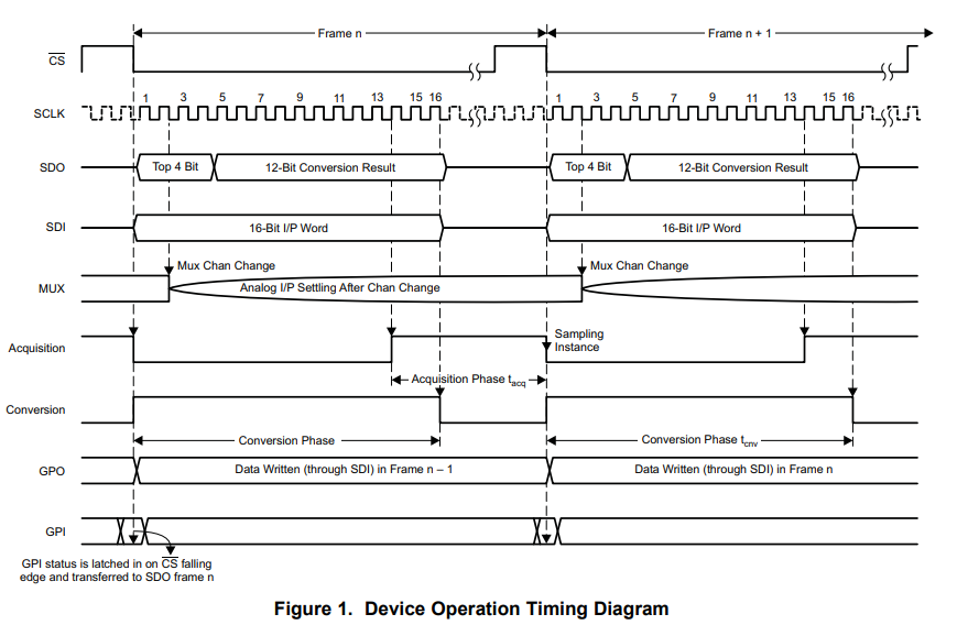
endmodule