This thread has been locked.

If you have a related question, please click the "Ask a related question" button in the top right corner. The newly created question will be automatically linked to this question.

[参考译文] SM73201:使用 Arduino 读取 ADC 时出现问题

Guru**** 2378660 points
请注意,本文内容源自机器翻译,可能存在语法或其它翻译错误,仅供参考。如需获取准确内容,请参阅链接中的英语原文或自行翻译。

https://e2e.ti.com/support/data-converters-group/data-converters/f/data-converters-forum/870682/sm73201-problem-to-read-adc-by-using-arduino

器件型号:SM73201

您好!

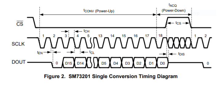
我正在尝试 使用 Arduino 读取 ADC SM 73201。 根据数据表、它是二进制补码二进制文件、您可以给我一些提示、告诉我如何读取 ADC 值并转换为电压。 我的基准电压为2.048。

谢谢

Ahmed

  • 请注意,本文内容源自机器翻译,可能存在语法或其它翻译错误,仅供参考。如需获取准确内容,请参阅链接中的英语原文或自行翻译。

    您好、Ahmed、

    欢迎访问 TI E2E 社区。

    首先、由于您使用的是2.048V 基准电压、因此满量程输入范围将是-2.048V 至+2.048V 差分电压。  如果您按照数据表中的图30连接单端输入的输入、并将负输入(引脚3)设置为2.048V、然后正输入(引脚2)为0V、则 ADC 看到的差分电压将读数为-2.048V 或负满量程。  正输入为4.096V 时、ADC 看到的差分电压读数将为+2.048V 或正满量程。

    对于 SPI 通信、您需要使用 IO 引脚将/CS 拉低(当/CS 拉低时、SCLK 应为高电平)、然后提供18个 SCLK 以获得完整的16b 转换结果。  前两位被丢弃、MSB (二进制补码读数的符号位)将在第三个 SCLK 下降沿启动、并可在第三个 SCLK 上升沿由主机 MCU 捕获。

    一旦您获得小数范围为-32768至+32767的16b 有符号整数(代码)、您就可以按如下方式计算输入电压:

    Vinput = code/32768*Vref

    对于十进制代码10、000、输入电压将为 Vin=10000/32768*2.048V=+0.625V。  相对于接地测量时、ADC 输入端的实际电压为-IN=+2.048V 和+IN=+2.673V。

    此致、
    Keith Nicholas
    精密 ADC 应用

  • 请注意,本文内容源自机器翻译,可能存在语法或其它翻译错误,仅供参考。如需获取准确内容,请参阅链接中的英语原文或自行翻译。

    Nicholas、您好!

    感谢您的详细回答。 我将尝试使用您的指令并使用我的代码来联系您。

    此致

    Ahmed

  • 请注意,本文内容源自机器翻译,可能存在语法或其它翻译错误,仅供参考。如需获取准确内容,请参阅链接中的英语原文或自行翻译。

    Nicholas、您好!

    请查看下面的代码、但我在串行端口上没有看到任何内容。 我正在使用 Arduino Micro 32U4控制器。 实际上、我想读取步长为30uV 的0至1mV 信号。 我已经完成了我的硬件部分并尝试使用编程进行读取。 接下来、我将对 CS 使用多路复用器74HC154、并通过使用单一 Arduino 读取12个差分 ADC。 在这方面需要您的帮助、并指导我如何在您以前读 ADC 时创建单/双时钟脉冲延迟。

    Ahmed

    #include <SPI.h>

    /* SPI Pins used:
      MISO = 11
      SCK = 9
      CS = 27
      */


    const int CS = 27; //Chip select output. Controls the slave device

    int adcValue=0;//This is the value in the ADC output register
    byte dummyByte;//Byte that does nothing but allows the conversion cycle to complete.
    byte upperByte;//Most significant BIT
    byte lowerByte;//Least significant BIT


    void setup(){
     SPI.begin();//Enables the SPI interface
     SPI.setDataMode(SPI_MODE0);
      pinMode(adcCS, OUTPUT);

       Serial.begin(9600);

     
    //Reset cycle for the ADC. Initializes the chip on power up. Occurs only 1 time.  
    digitalWrite (CS, LOW);
    dummyByte = SPI.transfer(0); // Initialization/Reset clocks
    digitalWrite (CS,  HIGH);
     
    }
     
     void loop(){
       // read out data from prior conversion, provide clocks for next conversion

    digitalWrite (CS, LOW); //Enables SPI
    upperByte = SPI.transfer(0);  // read one byte of result back
    lowerByte = SPI.transfer(0);  // read one byte of result back
    dummyByte = SPI.transfer(0); // finish providing 18 clocks to complete conversion
    digitalWrite (CS,  HIGH); //Disables SPI
    adcValue = (upperByte<<8) + lowerByte; // Moves the upperByte to the left, then adds
                                     //the lowerByte.  Combining the two equals the adcValue.


    Serial.println(adcValue, DEC);//Prints the ADC Value to Serial port.
    float voltage = adcvalue * (2.048 / 65535.0);
    Serial.println(voltage);//Prints the ADC Value to Serial port.
                                     

       delay(250);
    }
  • 请注意,本文内容源自机器翻译,可能存在语法或其它翻译错误,仅供参考。如需获取准确内容,请参阅链接中的英语原文或自行翻译。

    您好、Ahmed、

    我不精通 Arduino,但如果我遵循以上代码,则需要按以下方式进行修改。

    结果的6个 MSB 将位于 UpperByte 中、低字节中接下来的8位以及 dummyByte 中的2个 LSB。

    对于 UpperByte、您需要向左移动10、而不是8。  低位字节需要向左移位2、而 dummyByte 需要向右移位6。  然后、您将合并(或)所有三个值以获得最终结果。  如果 adcValue 为32b 整数、则需要强制上部16位为0、因为 ADC 的第一个位输出是浮动的、并且可能随机读回为0或1。


    此致、

    Keith