Other Parts Discussed in Thread: LP-MSP430FR2476, TCAN4550
请注意,本文内容源自机器翻译,可能存在语法或其它翻译错误,仅供参考。如需获取准确内容,请参阅链接中的英语原文或自行翻译。
部件号:LP-MSP430FR2476 “线程: TCAN4550”中讨论的其它部件
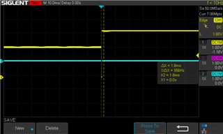
我正在尝试将 TCAN4550项目用于 LP-MSP430FR2476引脚。 我不确定 SPI 设置是否正确。 我没有看到 SPI CS 在范围上激活。 欣赏指针。 SPI 的时钟源为16 MHz。
#include <msp430.h>
#include "globals.h"
#include "clock~.h"
#define SPI_MOSI_PORT GPIO_PORT_P3
#define SPI_MOSI_PIN GPIO_PIN2
#define SPI_MISO_PORT GPIO_PORT_P3
#define SPI_MISO_PIN GPIO_PIN6
#define SPI_CLK_PORT GPIO_PORT_P3
#define SPI_CLK_PIN GPIO_PIN5
#define SPI_CS_PORT GPIO_PORT_P2
#define SPI_CS_PIN GPIO_PIN7
#define SPI_SELECT_FUNCTION GPIO_PRIMARY_MODULE_FUNCTION
volatile uint8_t TCAN_Int_Cnt = 0; // A variable used to keep track of interrupts the MCAN Interrupt pin
void init_spi_peripheral(){
GPIO_setAsPeripheralModuleFunctionOutputPin(SPI_MOSI_PORT, SPI_MOSI_PIN, SPI_SELECT_FUNCTION);
GPIO_setAsPeripheralModuleFunctionInputPin(SPI_MISO_PORT, SPI_MISO_PIN, SPI_SELECT_FUNCTION);
GPIO_setAsPeripheralModuleFunctionOutputPin(SPI_CLK_PORT, SPI_CLK_PIN, SPI_SELECT_FUNCTION);
GPIO_setAsPeripheralModuleFunctionOutputPin(SPI_CS_PORT, SPI_CS_PIN, SPI_SELECT_FUNCTION);
//Initialize Master
EUSCI_B_SPI_initMasterParam param = {0};
param.selectClockSource = EUSCI_B_SPI_CLOCKSOURCE_SMCLK;
param.clockSourceFrequency = CS_getSMCLK();
param.desiredSpiClock = 2000000;
param.msbFirst=EUSCI_B_SPI_MSB_FIRST;
param.clockPhase=EUSCI_B_SPI_PHASE_DATA_CAPTURED_ONFIRST_CHANGED_ON_NEXT;
param.clockPolarity=EUSCI_B_SPI_CLOCKPOLARITY_INACTIVITY_LOW;
param.spiMode=EUSCI_B_SPI_4PIN_UCxSTE_ACTIVE_HIGH;
EUSCI_B_SPI_initMaster(EUSCI_B1_BASE, ¶m);
EUSCI_B_SPI_select4PinFunctionality(EUSCI_B1_BASE,0x00);
EUSCI_B_SPI_enable(EUSCI_B1_BASE);
}
/**
* Initialize system clocks
*/
static void init_clock(void) {
// Configure one FRAM waitstate as required by the device datasheet for MCLK
// operation beyond 8MHz _before_ configuring the clock system.
FRAMCtl_configureWaitStateControl(FRAMCTL_ACCESS_TIME_CYCLES_1);
//Set DCO FLL reference = REFO
CS_initClockSignal(CS_FLLREF, CS_REFOCLK_SELECT, CS_CLOCK_DIVIDER_1);
//Set ACLK = REFO
CS_initClockSignal(CS_ACLK, CS_REFOCLK_SELECT, CS_CLOCK_DIVIDER_1);
CS_initFLLParam param = {0};
//Set Ratio/Desired MCLK Frequency, initialize DCO, save trim values
CS_initFLLCalculateTrim(CS_MCLK_DESIRED_FREQUENCY_IN_KHZ, CS_MCLK_FLLREF_RATIO, ¶m);
//Set MCLK = REFO
CS_initClockSignal(CS_MCLK, CS_REFOCLK_SELECT, CS_CLOCK_DIVIDER_1);
//Set SMCLK = DCO
CS_initClockSignal(CS_SMCLK, CS_DCOCLKDIV_SELECT, CS_CLOCK_DIVIDER_1);
//Clear all OSC fault flag
CS_clearAllOscFlagsWithTimeout(1000);
}
/*
* Configure the TCAN4550
*/
void
init_can(void)
{
TCAN4x5x_Device_ClearSPIERR(); // Clear any SPI ERR flags that might be set as a result of our pin mux changing during MCU startup
/* Step one attempt to clear all interrupts */
TCAN4x5x_Device_Interrupt_Enable dev_ie = {0}; // Initialize to 0 to all bits are set to 0.
TCAN4x5x_Device_ConfigureInterruptEnable(&dev_ie); // Disable all non-MCAN related interrupts for simplicity
TCAN4x5x_Device_Interrupts dev_ir = {0}; // Setup a new MCAN IR object for easy interrupt checking
TCAN4x5x_Device_ReadInterrupts(&dev_ir); // Request that the struct be updated with current DEVICE (not MCAN) interrupt values
if (dev_ir.PWRON) // If the Power On interrupt flag is set
TCAN4x5x_Device_ClearInterrupts(&dev_ir); // Clear it because if it's not cleared within ~4 minutes, it goes to sleep
/* Configure the CAN bus speeds */
TCAN4x5x_MCAN_Nominal_Timing_Simple TCANNomTiming = {0}; // 500k arbitration with a 40 MHz crystal ((40E6 / 2) / (32 + 8) = 500E3)
TCANNomTiming.NominalBitRatePrescaler = 2;
TCANNomTiming.NominalTqBeforeSamplePoint = 32;
TCANNomTiming.NominalTqAfterSamplePoint = 8;
TCAN4x5x_MCAN_Data_Timing_Simple TCANDataTiming = {0}; // 2 Mbps CAN FD with a 40 MHz crystal (40E6 / (15 + 5) = 2E6)
TCANDataTiming.DataBitRatePrescaler = 1;
TCANDataTiming.DataTqBeforeSamplePoint = 15;
TCANDataTiming.DataTqAfterSamplePoint = 5;
/* Configure the MCAN core settings */
TCAN4x5x_MCAN_CCCR_Config cccrConfig = {0}; // Remember to initialize to 0, or you'll get random garbage!
cccrConfig.FDOE = 1; // CAN FD mode enable
cccrConfig.BRSE = 1; // CAN FD Bit rate switch enable
/* Configure the default CAN packet filtering settings */
TCAN4x5x_MCAN_Global_Filter_Configuration gfc = {0};
gfc.RRFE = 1; // Reject remote frames (TCAN4x5x doesn't support this)
gfc.RRFS = 1; // Reject remote frames (TCAN4x5x doesn't support this)
gfc.ANFE = TCAN4x5x_GFC_ACCEPT_INTO_RXFIFO0; // Default behavior if incoming message doesn't match a filter is to accept into RXFIO0 for extended ID messages (29 bit IDs)
gfc.ANFS = TCAN4x5x_GFC_ACCEPT_INTO_RXFIFO0; // Default behavior if incoming message doesn't match a filter is to accept into RXFIO0 for standard ID messages (11 bit IDs)
/* ************************************************************************
* In the next configuration block, we will set the MCAN core up to have:
* - 1 SID filter element
* - 1 XID Filter element
* - 5 RX FIFO 0 elements
* - RX FIFO 0 supports data payloads up to 64 bytes
* - RX FIFO 1 and RX Buffer will not have any elements, but we still set their data payload sizes, even though it's not required
* - No TX Event FIFOs
* - 2 Transmit buffers supporting up to 64 bytes of data payload
*/
TCAN4x5x_MRAM_Config MRAMConfiguration = {0};
MRAMConfiguration.SIDNumElements = 1; // Standard ID number of elements, you MUST have a filter written to MRAM for each element defined
MRAMConfiguration.XIDNumElements = 1; // Extended ID number of elements, you MUST have a filter written to MRAM for each element defined
MRAMConfiguration.Rx0NumElements = 5; // RX0 Number of elements
MRAMConfiguration.Rx0ElementSize = MRAM_64_Byte_Data; // RX0 data payload size
MRAMConfiguration.Rx1NumElements = 0; // RX1 number of elements
MRAMConfiguration.Rx1ElementSize = MRAM_64_Byte_Data; // RX1 data payload size
MRAMConfiguration.RxBufNumElements = 0; // RX buffer number of elements
MRAMConfiguration.RxBufElementSize = MRAM_64_Byte_Data; // RX buffer data payload size
MRAMConfiguration.TxEventFIFONumElements = 0; // TX Event FIFO number of elements
MRAMConfiguration.TxBufferNumElements = 2; // TX buffer number of elements
MRAMConfiguration.TxBufferElementSize = MRAM_64_Byte_Data; // TX buffer data payload size
/* Configure the MCAN core with the settings above, the changes in this block are write protected registers, *
* so it makes the most sense to do them all at once, so we only unlock and lock once */
TCAN4x5x_MCAN_EnableProtectedRegisters(); // Start by making protected registers accessible
TCAN4x5x_MCAN_ConfigureCCCRRegister(&cccrConfig); // Enable FD mode and Bit rate switching
TCAN4x5x_MCAN_ConfigureGlobalFilter(&gfc); // Configure the global filter configuration (Default CAN message behavior)
TCAN4x5x_MCAN_ConfigureNominalTiming_Simple(&TCANNomTiming);// Setup nominal/arbitration bit timing
TCAN4x5x_MCAN_ConfigureDataTiming_Simple(&TCANDataTiming); // Setup CAN FD timing
TCAN4x5x_MRAM_Clear(); // Clear all of MRAM (Writes 0's to all of it)
TCAN4x5x_MRAM_Configure(&MRAMConfiguration); // Set up the applicable registers related to MRAM configuration
TCAN4x5x_MCAN_DisableProtectedRegisters(); // Disable protected write and take device out of INIT mode
/* Set the interrupts we want to enable for MCAN */
TCAN4x5x_MCAN_Interrupt_Enable mcan_ie = {0}; // Remember to initialize to 0, or you'll get random garbage!
mcan_ie.RF0NE = 1; // RX FIFO 0 new message interrupt enable
TCAN4x5x_MCAN_ConfigureInterruptEnable(&mcan_ie); // Enable the appropriate registers
/* Setup filters, this filter will mark any message with ID 0x055 as a priority message */
TCAN4x5x_MCAN_SID_Filter SID_ID = {0};
SID_ID.SFT = TCAN4x5x_SID_SFT_CLASSIC; // SFT: Standard filter type. Configured as a classic filter
SID_ID.SFEC = TCAN4x5x_SID_SFEC_PRIORITYSTORERX0; // Standard filter element configuration, store it in RX fifo 0 as a priority message
SID_ID.SFID1 = 0x055; // SFID1 (Classic mode Filter)
SID_ID.SFID2 = 0x7FF; // SFID2 (Classic mode Mask)
TCAN4x5x_MCAN_WriteSIDFilter(0, &SID_ID); // Write to the MRAM
/* Store ID 0x12345678 as a priority message */
TCAN4x5x_MCAN_XID_Filter XID_ID = {0};
XID_ID.EFT = TCAN4x5x_XID_EFT_CLASSIC; // EFT
XID_ID.EFEC = TCAN4x5x_XID_EFEC_PRIORITYSTORERX0; // EFEC
XID_ID.EFID1 = 0x12345678; // EFID1 (Classic mode filter)
XID_ID.EFID2 = 0x1FFFFFFF; // EFID2 (Classic mode mask)
TCAN4x5x_MCAN_WriteXIDFilter(0, &XID_ID); // Write to the MRAM
/* Configure the TCAN4550 Non-CAN-related functions */
TCAN4x5x_DEV_CONFIG devConfig = {0}; // Remember to initialize to 0, or you'll get random garbage!
devConfig.SWE_DIS = 0; // Keep Sleep Wake Error Enabled (it's a disable bit, not an enable)
devConfig.DEVICE_RESET = 0; // Not requesting a software reset
devConfig.WD_EN = 0; // Watchdog disabled
devConfig.nWKRQ_CONFIG = 0; // Mirror INH function (default)
devConfig.INH_DIS = 0; // INH enabled (default)
devConfig.GPIO1_GPO_CONFIG = TCAN4x5x_DEV_CONFIG_GPO1_MCAN_INT1; // MCAN nINT 1 (default)
devConfig.FAIL_SAFE_EN = 0; // Failsafe disabled (default)
devConfig.GPIO1_CONFIG = TCAN4x5x_DEV_CONFIG_GPIO1_CONFIG_GPO; // GPIO set as GPO (Default)
devConfig.WD_ACTION = TCAN4x5x_DEV_CONFIG_WDT_ACTION_nINT; // Watchdog set an interrupt (default)
devConfig.WD_BIT_RESET = 0; // Don't reset the watchdog
devConfig.nWKRQ_VOLTAGE = 0; // Set nWKRQ to internal voltage rail (default)
devConfig.GPO2_CONFIG = TCAN4x5x_DEV_CONFIG_GPO2_NO_ACTION; // GPO2 has no behavior (default)
devConfig.CLK_REF = 1; // Input crystal is a 40 MHz crystal (default)
devConfig.WAKE_CONFIG = TCAN4x5x_DEV_CONFIG_WAKE_BOTH_EDGES;// Wake pin can be triggered by either edge (default)
TCAN4x5x_Device_Configure(&devConfig); // Configure the device with the above configuration
TCAN4x5x_Device_SetMode(TCAN4x5x_DEVICE_MODE_NORMAL); // Set to normal mode, since configuration is done. This line turns on the transceiver
TCAN4x5x_MCAN_ClearInterruptsAll(); // Resets all MCAN interrupts (does NOT include any SPIERR interrupts)
}
/*
* GPIO Initialization
*/
void
init_gpio()
{
GPIO_setAsOutputPin( GPIO_PORT_P1, GPIO_PIN_ALL8);
GPIO_setAsOutputPin( GPIO_PORT_P2, GPIO_PIN_ALL8);
GPIO_setAsOutputPin( GPIO_PORT_P3, GPIO_PIN_ALL8);
GPIO_setAsOutputPin( GPIO_PORT_P4, GPIO_PIN_ALL8);
GPIO_setAsOutputPin( GPIO_PORT_P5, GPIO_PIN_ALL8);
GPIO_setAsOutputPin( GPIO_PORT_P6, GPIO_PIN0 | GPIO_PIN1 | GPIO_PIN2);
// Set all GPIO pins to output low to prevent floating input and reduce power consumption
GPIO_setOutputLowOnPin(GPIO_PORT_P1, GPIO_PIN_ALL8);
GPIO_setOutputHighOnPin(GPIO_PORT_P2, GPIO_PIN_ALL8);
GPIO_setOutputLowOnPin(GPIO_PORT_P3, GPIO_PIN_ALL8);
GPIO_setOutputLowOnPin(GPIO_PORT_P4, GPIO_PIN_ALL8);
GPIO_setOutputLowOnPin(GPIO_PORT_P5, GPIO_PIN_ALL8);
GPIO_setOutputLowOnPin(GPIO_PORT_P6, GPIO_PIN0 | GPIO_PIN1 | GPIO_PIN2);
// Configure P4.2 input for CAN interrupt
GPIO_setAsInputPinWithPullUpResistor(GPIO_PORT_P4, GPIO_PIN2);
GPIO_selectInterruptEdge(GPIO_PORT_P4, GPIO_PIN2, GPIO_HIGH_TO_LOW_TRANSITION);
GPIO_clearInterrupt(GPIO_PORT_P4, GPIO_PIN2);
GPIO_enableInterrupt(GPIO_PORT_P4, GPIO_PIN2);
GPIO_setOutputHighOnPin(GPIO_PORT_P4, GPIO_PIN1); //MCU P4.1 CAN reset pin
// Disable the GPIO power-on default high-impedance mode
// to activate previously configured port settings
PMM_unlockLPM5();
}
/**
* main.c
*/
int main(void)
{
WDTCTL = WDTPW | WDTHOLD; // stop watchdog timer
init_gpio(); // Set up GPIOs for SPI and TCAN4550 connections
init_clock(); // Set up the system clocks for 16 MHz (on the MSP430)
init_spi_peripheral(); // Initialize the SPI hardware module for 2 MHz SPI
GPIO_clearInterrupt(GPIO_PORT_P4, GPIO_PIN2); // Clear any interrupts on pin 4.2 before we enable global interrupts
__enable_interrupt();
init_can(); // Run the main MCAN configuration sequence. The bulk of the configuration is in this!
/* Define the CAN message we want to send*/
TCAN4x5x_MCAN_TX_Header header = {0}; // Remember to initialize to 0, or you'll get random garbage!
uint8_t data[4] = {0x55, 0x66, 0x77, 0x88}; // Define the data payload
header.DLC = MCAN_DLC_4B; // Set the DLC to be equal to or less than the data payload (it is ok to pass a 64 byte data array into the WriteTXFIFO function if your DLC is 8 bytes, only the first 8 bytes will be read)
header.id = 0x144; // Set the ID
header.FDF = 1; // CAN FD frame enabled
header.BRS = 1; // Bit rate switch enabled
header.EFC = 0;
header.MM = 0;
header.RTR = 0;
header.XTD = 0; // We are not using an extended ID in this example
header.ESI = 0; // Error state indicator
TCAN4x5x_MCAN_WriteTXBuffer(0, &header, data); // This function actually writes the header and data payload to the TCAN's MRAM in the specified TX queue number. It returns the bit necessary to write to TXBAR,
// but does not necessarily require you to use it. In this example, we won't, so that we can send the data queued up at a later point.
/* Let's make a different CAN message */
data[0] = 0x11;
data[1] = 0x22;
data[2] = 0x33;
data[3] = 0x44; // Define the data payload
header.DLC = MCAN_DLC_4B; // Set the DLC to be equal to or less than the data payload (it is ok to pass a 64 byte data array into the WriteTXFIFO function if your DLC is 8 bytes, only the first 8 bytes will be read)
header.id = 0x123; // Set the ID
header.FDF = 1; // CAN FD frame enabled
header.BRS = 1; // Bit rate switch enabled
header.EFC = 0;
header.MM = 0;
header.RTR = 0;
header.XTD = 0; // We are not using an extended ID in this example
header.ESI = 0; // Error state indicator
TCAN4x5x_MCAN_WriteTXBuffer(1, &header, data); // This line writes the data and header to TX FIFO 1
TCAN4x5x_MCAN_TransmitBufferContents(1); // Request that TX Buffer 1 be transmitted
TCAN4x5x_MCAN_TransmitBufferContents(0); // Now we can send the TX FIFO element 0 data that we had queued up earlier but didn't send.
while (1)
{
TCAN4x5x_MCAN_TransmitBufferContents(0); // Now we can send the TX FIFO element 0 data that we had queued up earlier but didn't send.
__delay_cycles(16000000);
if (TCAN_Int_Cnt > 0 )
{
TCAN_Int_Cnt--;
TCAN4x5x_Device_Interrupts dev_ir = {0}; // Define a new Device IR object for device (non-CAN) interrupt checking
TCAN4x5x_MCAN_Interrupts mcan_ir = {0}; // Setup a new MCAN IR object for easy interrupt checking
TCAN4x5x_Device_ReadInterrupts(&dev_ir); // Read the device interrupt register
TCAN4x5x_MCAN_ReadInterrupts(&mcan_ir); // Read the interrupt register
if (dev_ir.SPIERR) // If the SPIERR flag is set
TCAN4x5x_Device_ClearSPIERR(); // Clear the SPIERR flag
if (mcan_ir.RF0N) // If a new message in RX FIFO 0
{
TCAN4x5x_MCAN_RX_Header MsgHeader = {0}; // Initialize to 0 or you'll get garbage
uint8_t numBytes = 0; // Used since the ReadNextFIFO function will return how many bytes of data were read
uint8_t dataPayload[64] = {0}; // Used to store the received data
TCAN4x5x_MCAN_ClearInterrupts(&mcan_ir); // Clear any of the interrupt bits that are set.
numBytes = TCAN4x5x_MCAN_ReadNextFIFO( RXFIFO0, &MsgHeader, dataPayload); // This will read the next element in the RX FIFO 0
// numBytes will have the number of bytes it transfered in it. Or you can decode the DLC value in MsgHeader.DLC
// The data is now in dataPayload[], and message specific information is in the MsgHeader struct.
if (MsgHeader.id == 0x0AA) // Example of how you can do an action based off a received address
{
// Do something
}
}
}
}
}
//******************************************************************************
//
//This is the PORT2_VECTOR interrupt vector service routine
//
//******************************************************************************
#if defined(__TI_COMPILER_VERSION__) || defined(__IAR_SYSTEMS_ICC__)
#pragma vector=PORT4_VECTOR
__interrupt
#elif defined(__GNUC__)
__attribute__((interrupt(PORT4_VECTOR)))
#endif
void P4_ISR (void)
{
TCAN_Int_Cnt++;
GPIO_clearInterrupt (GPIO_PORT_P4, GPIO_PIN2);
// Toggle P1.0 output
GPIO_toggleOutputOnPin (GPIO_PORT_P1, GPIO_PIN0);
GPIO_setOutputHighOnPin(GPIO_PORT_P3, GPIO_PIN1);
}