This thread has been locked.

If you have a related question, please click the "Ask a related question" button in the top right corner. The newly created question will be automatically linked to this question.

[参考译文] MSP430F5659:LPM4低功耗模式电流消耗帮助。

Guru**** 2482105 points
Other Parts Discussed in Thread: MSP430F5659

请注意,本文内容源自机器翻译,可能存在语法或其它翻译错误,仅供参考。如需获取准确内容,请参阅链接中的英语原文或自行翻译。

https://e2e.ti.com/support/microcontrollers/msp-low-power-microcontrollers-group/msp430/f/msp-low-power-microcontroller-forum/1256029/msp430f5659-help-with-lpm4-low-power-mode-current-draw

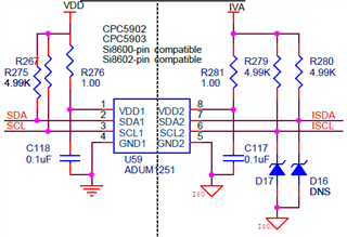
器件型号:MSP430F5659

目前、我们填充了 MSP430F5659上的每个端口、这可能是我将微控制器置于低功耗模式(LPM4状态)时、我们无法理解为什么会有显著的电流消耗。 当微控制器进入低功耗模式时、它消耗大约533uA 的电流。 它最初是从1.148 mA 获得的、但我通过发出以下命令"DAC12_1DAT = 0;"、将微控制器的值更改为"0"、从而降低了电流消耗。  下图是 MSP430F5659的布局、后跟将微控制器置于低功耗模式的主代码。 我注意到的一种奇怪现象是、当微控制器在低功耗模式下启动、等待中断退出低功耗模式时、微控制器消耗大约55uA 的电流。 首次上电和下电时、其低功耗模式约为550uA。 所以在未加电的情况下启动低功耗模式与微退出低功耗模式、然后重新置于低功耗模式之间似乎存在差异。 我已经在器件退出低功耗模式后删除了源代码、以隔离额外关断电流的来源。 这似乎来自加电功能、但将微控制器置于低功耗模式的大部分主代码应可缓解最初在加电功能中运行的任何问题。  


// Entering Low-Power Mode

P1IFG = 0;  // clear any pending interrupts
HW_CLEAR_SOURCE_READ_INTERRUPT;
HW_CLEAR_CHRG_ADAPT_INTERRUPT_FLAG;
DAC12_1DAT = 0;

HW_SSR_DRIVE_STRENGTH_LOW;      // Lower the drive strength from ports (P3.2, P8.7, P8.4, P7.4)

_EINT();

DISABLE_WATCHDOG; 		// WDTCTL = WDTPW + WDTHOLD;  // disable Watchdog
WriteFlash(EZ_CHECKS);

// Port Configuration
P1DIR = 0xFF;
P1OUT = 0x00;
P1IE = 0x00;  //Port1 is not interruptable.
P1IES = 0x00;  //Interrupt on low-to-high.
P1SEL = 0x00;  //No functions on port1.

P2DIR = 0xFF;  //Port2 is output selected.
P2OUT = 0x00;
P2IE = 0x00;  //Port2 is not interruptable.
P2IES = 0x00;  //Interrupt on low-to-high.
P2SEL = 0x00;  //No functions on port2.

P3DIR = 0xFF;
P3OUT = 0x00;
P3SEL = 0x00;  //No functions on port3.
P3IES = 0x00;  //Interrupt on low-to-high.
P3SEL = 0x00;  //No functions on port1.

P4DIR = 0xFF;  //Port4 is output selected.
P4OUT = 0x00;
P4SEL = 0x00;  //No functions on port4.

P5DIR = 0xFF;  //Port5 is output selected.
P5OUT = 0x00;
P5SEL = 0x00;  //No functions on port5.
 
P6DIR = 0xFF;  //Port6 is output selected.                      
P6OUT = 0x00;
P6SEL = 0x00;  //No functions on port6.
 
P7DIR = 0xFF;  //Port7 is output selected, power control		
P7OUT = 0x00;
P7SEL = 0x00;  //No functions on port7.
 
P8DIR = 0xFF;
P8OUT = 0x00;
P8SEL = 0x00;  //No functions on port8.
 
P9DIR = 0xFF;
P9OUT = 0x00;
P9SEL = 0x00;  //No functions on port9.
 
PJDIR = 0xFF;  //PortJ is input selected.
PJOUT = 0x00;

HW_ENABLE_SWITCH_INTERRUPTS;		// enable source/read switch interrupts


// Setup UCS
UCSCTL4 = SELA_1 + SELS_1 + SELM_1;                       // Ensure VLO is  every CLK source

UCSCTL6 |= XT2OFF + XT1OFF;// + SMCLKOFF;					// make sure XT1 and XT2 are off
UCSCTL8 &= ~(MODOSCREQEN  + SMCLKREQEN + MCLKREQEN + ACLKREQEN); // Clear clock requests so lpm can properly be entered

// Disable VUSB LDO and SLDO
USBKEYPID   =     0x9628;                 // set USB KEYandPID to 0x9628
                                    // enable access to USB config reg
USBPWRCTL &= ~(SLDOEN+VUSBEN);            // Disable the VUSB LDO and the SLDO
USBKEYPID   =    0x9600;                  // disable access to USB config reg


// Setup ADC
ADC12CTL0 &= ~ADC12ON;               //ADC12 is OFF
PMMCTL0_H = PMMPW_H;                    // PMM Password

// Disable SVS
SVSMHCTL &= ~(SVMHE | SVSHE);           // Disable High side SVS
SVSMLCTL &= ~(SVMLE | SVSLE);           // Disable Low side SVS

__bis_SR_register(LPM4_bits + GIE); // Enter low power mode 4 with interrupts enabled
UCSCTL8 |= (SMCLKREQEN + MCLKREQEN + ACLKREQEN); // enable clock requests so lpm can properly be exited

  • 请注意,本文内容源自机器翻译,可能存在语法或其它翻译错误,仅供参考。如需获取准确内容,请参阅链接中的英语原文或自行翻译。

    将引脚更改为输出至少是问题的一部分。 您不会展示他们连接到什么、因此我不知道问题到底有多大。 但有几个信号名称出现了一个问题:端口2上的 SDAB 和 SCLB。

    看起来类似于 I2C 连接、这意味着存在上拉电阻器、因此将引脚从端口功能切换到输出(低电平)将导致从这些上拉电阻器灌入电流。 将引脚保留在端口功能上会使引脚处于正常的低电流开漏状态。

  • 请注意,本文内容源自机器翻译,可能存在语法或其它翻译错误,仅供参考。如需获取准确内容,请参阅链接中的英语原文或自行翻译。

    因此我将您启动的端口(SDAB 和 SCLB)从输出更改为输入。 我仍然没有看到我们的器件上的关断电流发生变化。  我还附上了每个端口的列表以及该端口在我们的器件上的功能、以便您更好地了解该端口。 当微控制器处于低功耗模式时、VDD 不上电、充当 SDAB、SCLB、SDA 和 SCL 的上拉电压。 请告诉我、如果其他任何不适当的声音可能会产生额外的关断电流。  


    // Port 1
    FCLK 	// isn't used on this board yet.
    ENC+	// is used as an input from a peripheral device when the micro is ON.
    ENC- 	// is used as an input from a peripheral device when the micro is ON.
    SW		// is used as an input from a peripheral device when the micro is ON.
    SRCE	// is used as an interrupt from a peripheral device to turn the micro ON or put it in Low-Power Mode.
    FIN 	// isn't used on this board yet.
    HI		// is used as an input from a peripheral device to change the state on the board when ON.
    LO		// is used as an input from a peripheral device to change the state on the board when ON.
    
    // Port 2
    FIN		// isn't used on this board yet.
    SDAB	// is used for I2C, there is no pull up voltage on this line when the micro is not ON or when the micro is in Low-Power Mode.
    SCLB	// is used for I2C, there is no pull up voltage on this line when the micro is not ON or when the micro is in Low-Power Mode.
    READ	// is used as an interrupt from a peripheral device to turn the micro ON or put it in Low-Power Mode.
    IVSRC	// is used as an output to control an opto isolator. 
    X1		// is used as an output, but it isn't on this board yet. 
    OVLD	// isn't used on this board yet.
    SW	 	// is used as an input from a peripheral device when the micro is ON.
    
    // Port 3
    ADTR	// is used as an interrupt to wake up the micro from Low-Power Mode. 
    TONE	// isn't used on this board yet. 
    IVRD	// is used as an output to control a relay.
    HART	// is used as an output to control a relay.
    VG2		// is used as an output to control a relay.
    485DE	// is used as an output.
    LWPR	// is used as an output.
    FSYN	// isn't used on this board yet. 
    
    // Port 4
    DB0		// is an output used to control a LCD Display.
    DB1		// is an output used to control a LCD Display.
    DB2		// is an output used to control a LCD Display.
    DB3		// is an output used to control a LCD Display.
    DB4		// is an output used to control a LCD Display.
    DB5		// is an output used to control a LCD Display.
    DB6		// is an output used to control a LCD Display.
    DB7		// is an output used to control a LCD Display.
    
    // Port 5
    VG1		// is used as an output to control a relay.
    VCMP	// is used as an output to control a relay.
    CS		// is used to control an LCD Display.
    RST		// is used to control an LCD Display.
    RS		// is used to control an LCD Display.
    RW		// is used to control an LCD Display.
    EN 		// is used to control an LCD Display.
    CHRG	// is used as an input.
    
    // Port 6
    4WDET	// is an output, but not used on this device.
    3WDET	// is an output, but not used on this device.
    BSUP	// is used as an input to read the supply voltage.
    SRW		// is used as an output, not on this device.
    CAL		// is used as an input to change state of the device when the micro is powered ON.
    ASW1	// is used as an output, not on this device. 
    LADJ	// is used as an output to control the state of a switching regulator. 
    DAC1	// is used as an output to vary voltage when powered ON.
    
    // Port 7
    N/A (Port #13)	// isn't used on this board.
    N/A (Port #14)	// isn't used on this board.
    (Port #84)		// is used for the cyrstal on the micro. 
    (Port #85)		// is used for the cyrstal on the micro. 
    ISRC	// is used as an output to control opto isolator.
    RDW		// is used as an output to control a relay. 
    ADTR	// is used as an input to read ADC readings from an external voltage supply. 
    DACA	// is used as an output, not on this device. 
    
    // Port 8
    CHEN	// is used as an output, to control the operation of an external device.
    ASW2	// is used as an output, not on this device. 
    DRDY	// is used as an input, not on this device. 
    N/A (Port #61)	// isn't on this board. 
    IRD 	// is used as an output to control an opto isolator.
    SDA 	// is used for I2C, there is no pull up voltage on this line when the micro is not ON or when the micro is in Low-Power Mode.
    SCL     // is used for I2C, there is no pull up voltage on this line when the micro is not ON or when the micro is in Low-Power Mode.
    SRC   	// is used as an output, not on this device. 
    
    // Port 9
    5524 	// is used as an output, not on this device.
    PWR		// is used as an output, to power on VDD, the pull up voltage for I2C. 
    TXD.INT // is used as an output
    RXD.INT // is used as an input
    SCK 	// is used as an output, not on this device. 
    MOSI	// is used as an output, not on this device.
    MISO	// is used as an input, not on this device. 
    VINC	// is used as an output, not on this device. 

  • 请注意,本文内容源自机器翻译,可能存在语法或其它翻译错误,仅供参考。如需获取准确内容,请参阅链接中的英语原文或自行翻译。

    RXD.INT (P9.3)是否连接到任何部件? 通常另一端会将其驱动至高电平、因此将其驱动至低电平的端会产生总线冲突。

  • 请注意,本文内容源自机器翻译,可能存在语法或其它翻译错误,仅供参考。如需获取准确内容,请参阅链接中的英语原文或自行翻译。

    那么、您是否认为"RXD.INT"可能会在低功耗模式下产生高电流消耗? 如果是这种情况、您针对该问题的解决方案是否会在微控制器进入低功耗模式之前更改该端口(P9.3)的方向/输出?   

    下面是我们的原理图 LTC2876中与'RXD.INT'连接的组件的图像。 当微控制器进入低功耗模式时、VDD 没有电压。 因此 U17无法运行。  

  • 请注意,本文内容源自机器翻译,可能存在语法或其它翻译错误,仅供参考。如需获取准确内容,请参阅链接中的英语原文或自行翻译。

    为了隔离此建议、我从电路板中删除了 U17、并且在低功耗模式关闭电流中没有看到任何变化。

  • 请注意,本文内容源自机器翻译,可能存在语法或其它翻译错误,仅供参考。如需获取准确内容,请参阅链接中的英语原文或自行翻译。

    我仍然怀疑总线冲突、但 很难 猜到其他引脚的作用。  

    排除此类冲突的一种方法是逐个(或在二进制搜索中减半)删除 PxDIR=设置、以查看每个设置是否产生任何效果。 这有点乏味、但应该可以在半小时左右完成。  来自浮动(线控)输入引脚的电流将比来自总线冲突的电流小得多。

  • 请注意,本文内容源自机器翻译,可能存在语法或其它翻译错误,仅供参考。如需获取准确内容,请参阅链接中的英语原文或自行翻译。

    好的、我将执行此操作以查看是否有任何更改、我将在完成此任务时进行回复。

  • 请注意,本文内容源自机器翻译,可能存在语法或其它翻译错误,仅供参考。如需获取准确内容,请参阅链接中的英语原文或自行翻译。

    因此、我使用 PxDIR 将微控制器上的每个端口方向从输入翻转为输出。 我发现问题的唯一方面是输入信号 CHRG (P5.7)。 未设置为输出时、原始关闭电流将从100uA 上升到600uA。 电路板再次上电/断电时、它会在650uA 左右悬停。 连接到这个输入信号的电阻器已经从这个输入信号中移除。 仍不确定关断电流的来源、但在最初测量电流时、大部分电流来自 MSP430F5659。

    PU.1、PU.0、VUSB、V18、VSSU、 在低功耗模式下创建高电流消耗?

  • 请注意,本文内容源自机器翻译,可能存在语法或其它翻译错误,仅供参考。如需获取准确内容,请参阅链接中的英语原文或自行翻译。

    我必须服从其他人关于 USB 支持的意见(特别是它的 LPM 行为)。

    恐怕我输错了轨道——你在 LPM4中看到的电流消耗是多少?

  • 请注意,本文内容源自机器翻译,可能存在语法或其它翻译错误,仅供参考。如需获取准确内容,请参阅链接中的英语原文或自行翻译。

    在 LPM4模式下、我看到530 μ A。  

  • 请注意,本文内容源自机器翻译,可能存在语法或其它翻译错误,仅供参考。如需获取准确内容,请参阅链接中的英语原文或自行翻译。

    尊敬的 Robb:

    我想以此为基础提出几条建议、我认为您之所以不进入 LPM4、是因为外设正在请求时钟。 这可以是 ADC、USB 等。 我可以看到初始化已将外设"关闭"、但我怀疑外设在第一次唤醒后开启了。 这就是您从低电流开始的原因、然后在第一次唤醒后、电流处于高电平。

    可以执行以下检查来验证它是否为外设: 为 LPM4加载我们的示例代码。 代码非常简单、通过该代码、我们可以隔离其外设是开启/请求时钟还是某些硬件连接消耗了额外电流。 如果仍然存在高电流消耗、接下来将检查硬件连接。

    在硬件方面、我可以看一下未使用引脚的连接。 我在您的原理图中看到 USB 无源组件是 DNS、这意味着它们没有填充。 这会导致这些引脚悬空或"断开"、而不是建议的连接(例如、查看 VBUS、它会在您的原理图中悬空、如果不使用它、应该接地。)

    建议连接未使用的引脚、以保持可预测状态并避免任何意外的电流消耗。

    此致、

    卢克

  • 请注意,本文内容源自机器翻译,可能存在语法或其它翻译错误,仅供参考。如需获取准确内容,请参阅链接中的英语原文或自行翻译。

    是的、这可能是我的问题。 当我检查这些潜在问题时、我会再次回答。  

  • 请注意,本文内容源自机器翻译,可能存在语法或其它翻译错误,仅供参考。如需获取准确内容,请参阅链接中的英语原文或自行翻译。

    低功耗模式(LPM4)下大关断电流的解决方案是由于 VSSU、VBUS 和 USBID 在不使用时未接地、并且发现在进入低功耗模式前、内部 ADC 和 DAC 未关闭。 我认为这解决了我的问题。 我感谢为发现此问题提供的帮助和指导。