Other Parts Discussed in Thread: TRF7960A, MSPM0L1306, SYSCONFIG
请注意,本文内容源自机器翻译,可能存在语法或其它翻译错误,仅供参考。如需获取准确内容,请参阅链接中的英语原文或自行翻译。
器件型号:TRF7960A Thread: MSPM0L1306、 SysConfig 中讨论的其他器件
工具/软件:
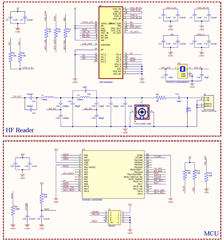
大家好、我制作了一个基于 TRF7960A 读取器并由 MSPM0L1306 MCU 控制的电路板、在上面、您可以看到此类电路板的原理图。 对于编码、我想分步进行、现在我尝试读取一个简单的寄存器值。 但我得到的响应始终是0x00 (可能是读取请求没有n´t 甚至没有到达 IC)。 通过 SysConfig 工具配置的 SPI 接口、无中断、2MHz 数据速率、Motorola 3线(我独立处理 CS 信号)、时钟极性和相位最初为0 (读取模式时、时钟极性变为1)。 我n´t 了 CLK、n´t 和 MOSI 内部下拉电阻器、因此当我禁用 SPI 以更改时钟极性时、它们不会进入高阻抗´s 状态(我不知道是否会出现这种情况)。 您能否帮助我识别和修复问题(也可能是硬件问题)?
#include "mspm0l130x.h"
#include "stdio.h"
#include "ti_msp_dl_config.h"

// Macros
#define HWREG(x) (*((volatile uint32_t *)(x)))

// Registers
#define Status_Control 0x00
#define ISO_Control 0x01
#define Tx_Pulse_Lenght_Ctrl 0x06
#define Rx_No_Resp_Wait_Time 0x07
#define Rx_Wait_Time_Register 0x08
#define Mod_Register 0x09
#define Rx_Special_Settings 0x0A
#define IRQ_Status 0x0C
#define IRQ_Mask 0x0D
#define FIFO_Status 0x1C
#define FIFO_Register 0x1F

// Constants
#define ISO14443A 0x08
#define OOK 0x21
#define Enable_RF 0x21
#define Disable_RF 0x01
#define Pulse_Lenght 0x20
#define No_Resp_Wait_Time 0x0E
#define Rx_Wait_Time 0x07
#define Special_Setting 0x20
#define IRQ_Mask_Set 0x3E
#define REQA_Command 0x26
#define ISO14443A_No_CRC 0x88
#define End_of_Tx_IRQ 0x80
#define End_of_Rx_IRQ 0x40
#define Collision_IRQ 0x02
#define SPI_Phase0 0x00000007
#define SPI_Phase1 0x00000207
#define SPI_Pol1 0x00000107
#define SPI_Pol0 0x00000007

// Direct Commands
#define SW_Init 0x03
#define Rst_FIFO 0x0F

// Function Prototypes
void TRF7960A_Init(void);
void TRF7960A_WriteRegister(uint8_t addr, uint8_t data);
uint8_t TRF7960A_ReadRegister(uint8_t addr);
void TRF7960A_DirectCommand(uint8_t cmd);

// Global variables
uint8_t reg_value = 2;

int main(void)
{
    SYSCFG_DL_init();

    DL_GPIO_setPins(TRF7960A_PINS_PORT, TRF7960A_PINS_SS_PIN); // SS to high

    TRF7960A_Init(); // Configuring TRF7960A

    while (1) {

        reg_value = TRF7960A_ReadRegister(ISO_Control);

        printf("%x\n", reg_value);

        delay_cycles(64000000); // 2s delay
    }

}

// Initializate TRF7960A
void TRF7960A_Init(void) {
    // ISO14443A configuration
    TRF7960A_DirectCommand(SW_Init); // Power Up
        delay_cycles(320000); // 10ms delay to wait for TRF7960A clock stabilization

    TRF7960A_WriteRegister(ISO_Control, ISO14443A); // ISO14443A 106kbps
    TRF7960A_WriteRegister(Mod_Register, OOK); // OOK (100%), 6.78MHz Clock (not used)
}

// Write in TRF7960A registers
void TRF7960A_WriteRegister(uint8_t addr, uint8_t data) {
    uint8_t cmd = (0x00 | addr) & 0x1F; // (0x00 | addr): B6 to Write Mode (0). (& 0x1F): To guarantee B4-B0 right address

    printf("%x\n", cmd);

    DL_GPIO_clearPins(TRF7960A_PINS_PORT, TRF7960A_PINS_SS_PIN); // SS to low
    DL_SPI_transmitDataBlocking8(SPI_0_INST, cmd); // Transmit the address of the desired register to write

    DL_SPI_transmitDataBlocking8(SPI_0_INST, data); // Write the desired value on the register

    DL_GPIO_setPins(TRF7960A_PINS_PORT, TRF7960A_PINS_SS_PIN); // SS to high
}

// Read a TRF7960A register
uint8_t TRF7960A_ReadRegister(uint8_t addr) {
    uint8_t cmd = (0x40 | addr) & 0x5F; // B6 to Read Mode (1). (& 0x5F): To guarantee B4-B0 right address
    uint8_t data = 1;

    printf("%x\n", cmd);

    DL_GPIO_clearPins(TRF7960A_PINS_PORT, TRF7960A_PINS_SS_PIN); // SS to low
    DL_SPI_transmitDataBlocking8(SPI_0_INST, cmd); // Transmit the address of the desired register to read

    DL_SPI_disable(SPI0);
    HWREG(SPI0_BASE + 0x1100) = SPI_Pol1; // SPI clock polarity = 1
    DL_SPI_enable(SPI0);

    data = DL_SPI_receiveDataBlocking8(SPI_0_INST);

    DL_SPI_disable(SPI0);
    HWREG(SPI0_BASE + 0x1100) = SPI_Pol0; // SPI clock polarity = 0
    DL_SPI_enable(SPI0);

    DL_GPIO_setPins(TRF7960A_PINS_PORT, TRF7960A_PINS_SS_PIN); // SS to high

    return data;
}