

请注意,本文内容源自机器翻译,可能存在语法或其它翻译错误,仅供参考。如需获取准确内容,请参阅链接中的英语原文或自行翻译。
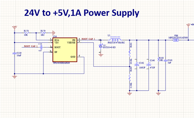
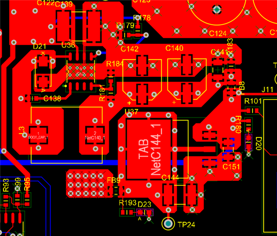
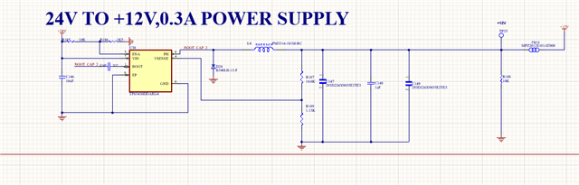
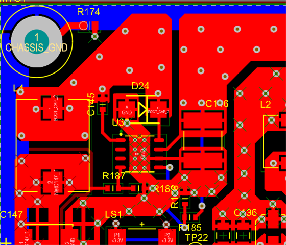
器件型号:TPS5430 大家好、
我们的客户希望申请对两个采用 TPS5430DDARG4的电源板进行 PCB 设计审查。 请参阅随附的原理图和 PCB 布局。
感谢您的支持!
此致、
Danilo
大家好、
我们的客户希望申请对两个采用 TPS5430DDARG4的电源板进行 PCB 设计审查。 请参阅随附的原理图和 PCB 布局。
感谢您的支持!
此致、
Danilo
