This thread has been locked.
If you have a related question, please click the "Ask a related question" button in the top right corner. The newly created question will be automatically linked to this question.
Other Parts Discussed in Thread: TPSM41615, TPSM41625
https://e2e.ti.com/support/power-management-group/power-management/f/power-management-forum/1006958/tpsm41615-layout-suggestion-of-tpsm41615
大家好、
我的客户正在评估我们的 TPSM41615、他们希望了解 TPSM41615的布局布局。
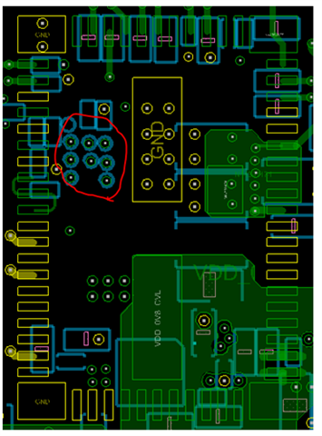
对于 TPSM41615的布局、是否可以将数字过孔置于 TPSM41615的封装之下?
您好!
我不建议在 TPSM41625下放置数字过孔。 封装的该区域有一些引脚对噪声敏感、 数据表中图10-3的布局建议在放置数字过孔的区域内、在器件下方的顶层保留一些引脚。
您好、Alec、
感谢你的帮助。 我正在查看客户 TPSM41615的布局。
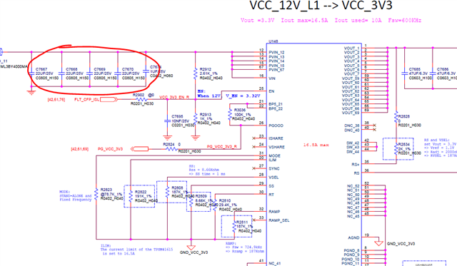
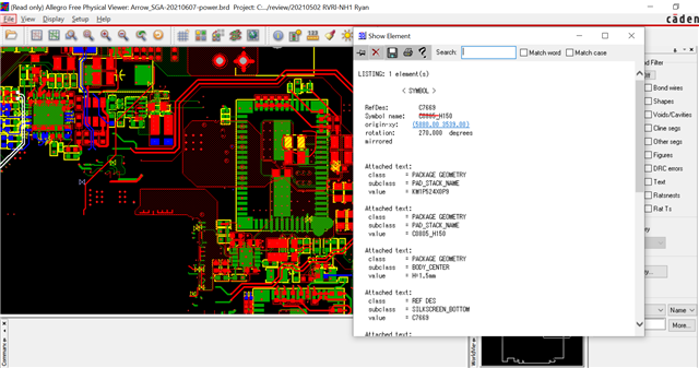
而且、它们已将 cin 放置在 模块的另一层 (TPSM41625)。 请参阅下图。 您是否会对此感到担忧?
在将 cin 电容器放置在电路板底层模块下方时、我没有太多顾虑。 请确保从底层到 PVIN 和 PGND 焊盘也有多个过孔。
此致、
Alec Biesterfeld