大家好、
我希望您能帮助我们澄清这一客户询问。
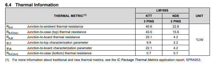
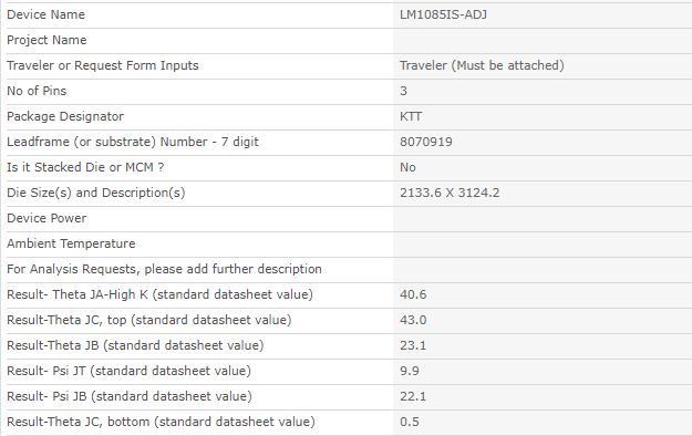
该模型具有3 C/W 的 θ JC 和3.043 C/W 的 θ JB
数据表中的 θ JC 为0.7 C/W、θ JB 为23.1 C/W
然而、PS VR2的标称功率为4W、这使得 DT 为92.4摄氏度
对于 θ JB、该值似乎很高。
非常感谢。
此致、
标记
This thread has been locked.
If you have a related question, please click the "Ask a related question" button in the top right corner. The newly created question will be automatically linked to this question.
您好!
使用3 C/W theta JC 和3.043 C/W theta JB 的模型 是 Raytheon 过去用于对该组件建模的历史值。 我正在尝试验证我们在对结至电路板建模时应使用的内容。 NDE 和 KTT 是否应具有该不同的耐受值? 许多组件制造商只会提供到外壳(底部)的 θ JC 值。 当它们给出一个 theta JB 值时、它们假定组件应该如何被安装到电路板上。 我只是想对这部分作出一些澄清。