This thread has been locked.
If you have a related question, please click the "Ask a related question" button in the top right corner. The newly created question will be automatically linked to this question.
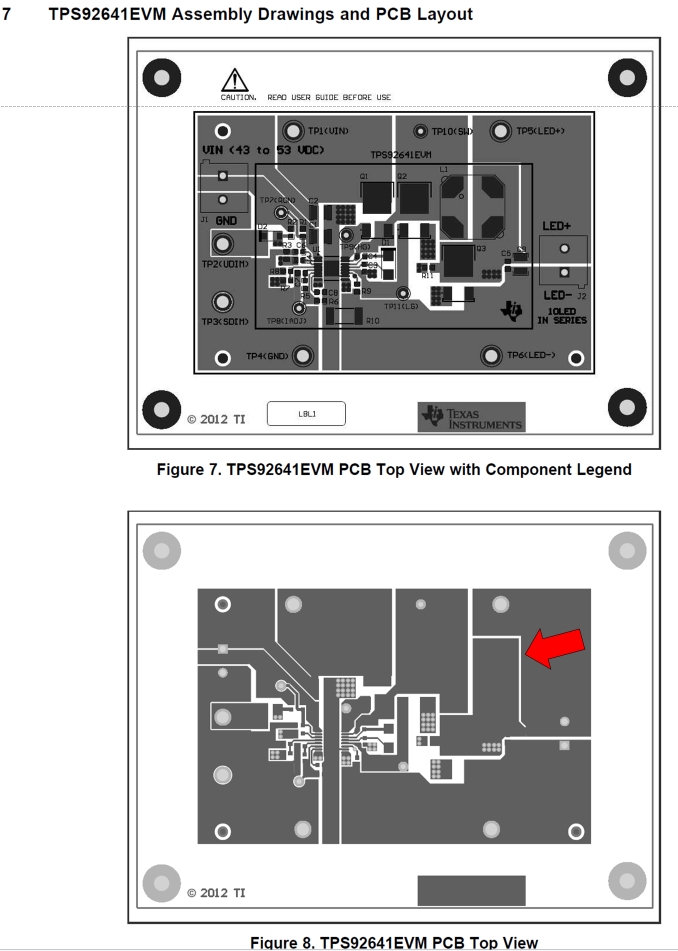
https://e2e.ti.com/support/power-management-group/power-management/f/power-management-forum/783984/tps92641evm-tricky-pcb-lay-out-between-inductor-and-power-output
我在 TPS92641EVM 的 LED+输出端找到了长缝隙。
我想知道狭缝的作用是什么?
(第10页、《TPS92641EVM 用户指南》、slvu823.pdf)