大家好!
我一直在诊断 BQ76942的严重问题。 我们将在少量原型板上熟悉并配置这些芯片。 我已成功准备好电池电压、温度值、电池组电流等。
我们通过 I2C 使用 STM32G474来控制芯片。 我使用了 STM32示例代码作为起点、这非常有帮助。
首先、我来说明一下我使用示例中提供的标准 BQInit 代码时出现的问题、不同之处在于我更改了 VCellMode 寄存器以反映电池组(4S)中的电池节数、从而使芯片不会引发 UV 错误。
代码的执行方式如下:首先释放 BQ_Reset 引脚、然后将 TS2引脚依次切换为低电平和高阻抗。 我在数据表中没有看到显示我应该切换此操作的任何内容、但它似乎是唯一唤醒芯片的东西。 然后、执行 BQReset 和 BQInit 函数。 在执行 INIT 禁用睡眠模式后、代码进入主循环。
在主循环中、我读取一些状态和错误寄存器、并每秒切换一次 DSGTEST 和 CHGTEST 命令。 读取 ReadFETStatus 函数和0x0057 Manufacturing Status 寄存器读取时、DSG 和 CHG 变量正在正确切换。 FET EN 位也会在该寄存器中取消置位、我认为这意味着器件处于测试模式。 测量电路板时、DSG FET 未完全关闭。 其栅极电压不上升到14伏以上(电池组电压为~14.7)。 在 CP1处测量的电荷泵在25.5伏和~14伏之间切换。 FET 启用时、电荷泵似乎正在关闭。
下面是代码:
void bmsInit()
{
	/* Initiate and set up the BMS hardware
	 * Load config data from EEPROM
	 * Read DIP switches and configure hardware
	 */

	if(__HAL_PWR_GET_FLAG(PWR_FLAG_SB) != RESET)
	{
		test = 1;
	}
	HAL_Delay(1);
	HAL_TIM_Base_Start_IT(&htim4);
	BQ769x2_ReleaseShutdownPin();//Release the BQ_Reset Pin
	delayUS(60000);
	HAL_GPIO_WritePin(GPIO2_GPIO_Port, GPIO2_Pin,GPIO_PIN_RESET);//Toggle the TS2 Pin Low
	delayUS(60000);
	HAL_GPIO_WritePin(GPIO2_GPIO_Port, GPIO2_Pin,GPIO_PIN_SET);//Toggle TS2 to high impedance
	// Initialize battery controller chip
	CommandSubcommands(BQ769x2_RESET);  // Resets the BQ769x2 registers
	delayUS(60000);
	BQ769x2_Init();  // Configure all of the BQ769x2 register settings
	delayUS(10000);
	CommandSubcommands(SLEEP_DISABLE); // Sleep mode is enabled by default. For this example, Sleep is disabled to demonstrate full-speed measurements in Normal mode.
	delayUS(60000); delayUS(60000); delayUS(60000); delayUS(60000);  //wait to start measurements after FETs close
void BQ769x2_Init() {
	// Configures all parameters in device RAM

	// Enter CONFIGUPDATE mode (Subcommand 0x0090) - It is required to be in CONFIG_UPDATE mode to program the device RAM settings
	// See TRM for full description of CONFIG_UPDATE mode
	CommandSubcommands(SET_CFGUPDATE);

	// After entering CONFIG_UPDATE mode, RAM registers can be programmed. When programming RAM, checksum and length must also be
	// programmed for the change to take effect. All of the RAM registers are described in detail in the BQ769x2 TRM.
	// An easier way to find the descriptions is in the BQStudio Data Memory screen. When you move the mouse over the register name,
	// a full description of the register and the bits will pop up on the screen.

	// 'Power Config' - 0x9234 = 0x2D80
	// Setting the DSLP_LDO bit allows the LDOs to remain active when the device goes into Deep Sleep mode
  	// Set wake speed bits to 00 for best performance
	BQ769x2_SetRegister(PowerConfig, 0x2D80, 2);

	// 'REG0 Config' - set REG0_EN bit to enable pre-regulator
	BQ769x2_SetRegister(REG0Config, 0x01, 1);

	// 'REG12 Config' - Enable REG1 with 3.3V output (0x0D for 3.3V, 0x0F for 5V)
	BQ769x2_SetRegister(REG12Config, 0x0D, 1);

	// Set DFETOFF pin to control BOTH CHG and DSG FET - 0x92FB = 0x42 (set to 0x00 to disable)
	BQ769x2_SetRegister(DFETOFFPinConfig, 0x42, 1);

	// Set up ALERT Pin - 0x92FC = 0x2A
	// This configures the ALERT pin to drive high (REG1 voltage) when enabled.
	// The ALERT pin can be used as an interrupt to the MCU when a protection has triggered or new measurements are available
	BQ769x2_SetRegister(ALERTPinConfig, 0x2A, 1);

	// Set TS1 to measure Cell Temperature - 0x92FD = 0x07
	BQ769x2_SetRegister(TS1Config, 0x07, 1);

	// Set TS3 to measure FET Temperature - 0x92FF = 0x0F
	BQ769x2_SetRegister(TS3Config, 0x0F, 1);

	// Set HDQ to measure Cell Temperature - 0x9300 = 0x07
	BQ769x2_SetRegister(HDQPinConfig, 0x00, 1);  // No thermistor installed on EVM HDQ pin, so set to 0x00

	// 'VCell Mode' - Enable 16 cells - 0x9304 = 0x0000; Writing 0x0000 sets the default of 16 cells
	BQ769x2_SetRegister(VCellMode, 0x0207, 2);

	// Enable protections in 'Enabled Protections A' 0x9261 = 0xBC
	// Enables SCD (short-circuit), OCD1 (over-current in discharge), OCC (over-current in charge),
	// COV (over-voltage), CUV (under-voltage)
	BQ769x2_SetRegister(EnabledProtectionsA, 0xBC, 1); //DISABLED, MUST BE REENABLED, OR ELSE

	// Enable all protections in 'Enabled Protections B' 0x9262 = 0xF7
	// Enables OTF (over-temperature FET), OTINT (internal over-temperature), OTD (over-temperature in discharge),
	// OTC (over-temperature in charge), UTINT (internal under-temperature), UTD (under-temperature in discharge), UTC (under-temperature in charge)
	BQ769x2_SetRegister(EnabledProtectionsB, 0xF7, 1);

	// 'Default Alarm Mask' - 0x..82 Enables the FullScan and ADScan bits, default value = 0xF800
	BQ769x2_SetRegister(DefaultAlarmMask, 0xF882, 2);

	// Set up Cell Balancing Configuration - 0x9335 = 0x03   -  Automated balancing while in Relax or Charge modes
	// Also see "Cell Balancing with BQ769x2 Battery Monitors" document on ti.com
	BQ769x2_SetRegister(BalancingConfiguration, 0x03, 1);

	// Set up CUV (under-voltage) Threshold - 0x9275 = 0x31 (2479 mV)
	// CUV Threshold is this value multiplied by 50.6mV
	BQ769x2_SetRegister(CUVThreshold, 0x31, 1);

	// Set up COV (over-voltage) Threshold - 0x9278 = 0x55 (4301 mV)
	// COV Threshold is this value multiplied by 50.6mV
	BQ769x2_SetRegister(COVThreshold, 0x55, 1);

	// Set up OCC (over-current in charge) Threshold - 0x9280 = 0x05 (10 mV = 10A across 1mOhm sense resistor) Units in 2mV
	BQ769x2_SetRegister(OCCThreshold, 0x05, 1);

	// Set up OCD1 Threshold - 0x9282 = 0x0A (20 mV = 20A across 1mOhm sense resistor) units of 2mV
	BQ769x2_SetRegister(OCD1Threshold, 0x0A, 1);

	// Set up SCD Threshold - 0x9286 = 0x05 (100 mV = 100A across 1mOhm sense resistor)  0x05=100mV
	BQ769x2_SetRegister(SCDThreshold, 0x05, 1);

	// Set up SCD Delay - 0x9287 = 0x03 (30 us) Enabled with a delay of (value - 1) * 15 µs; min value of 1
	BQ769x2_SetRegister(SCDDelay, 0x03, 1);

	// Set up SCDL Latch Limit to 1 to set SCD recovery only with load removal 0x9295 = 0x01
	// If this is not set, then SCD will recover based on time (SCD Recovery Time parameter).
	BQ769x2_SetRegister(SCDLLatchLimit, 0x01, 1);

	// Exit CONFIGUPDATE mode  - Subcommand 0x0092
	CommandSubcommands(EXIT_CFGUPDATE);
}
while (1)
  {
    /* USER CODE END WHILE */

    /* USER CODE BEGIN 3 */
	time = HAL_GetTick();

	BQ769x2_ReadPFStatus();
	BQ769x2_ReadFETStatus();
	wake_status = BQ769x2_ReadWakeStatus();

	if(time-last_switch_time>1000){
		CommandSubcommands(DSGTEST);
		CommandSubcommands(CHGTEST);
		last_switch_time = time;
	}

	BQ769x2_ReadManufacturingStatus();

	AlarmBits = BQ769x2_ReadAlarmStatus();
	if (AlarmBits & 0x80) {  // Check if FULLSCAN is complete. If set, new measurements are available
		BQ769x2_ReadAllVoltages();
		Pack_Current = BQ769x2_ReadCurrent();
		Temperature[0] = BQ769x2_ReadTemperature(TS1Temperature);
		Temperature[1] = BQ769x2_ReadTemperature(IntTemperature);
		DirectCommands(AlarmStatus, 0x0080, W_BQ);  // Clear the FULLSCAN bit
	}

	if (AlarmBits & 0xC000) {  // If Safety Status bits are showing in AlarmStatus register
		BQ769x2_ReadSafetyStatus(); // Read the Safety Status registers to find which protections have triggered
		if (ProtectionsTriggered & 1) {
			DirectCommands(AlarmStatus, 0xF800, W_BQ); // Clear the Safety Status Alarm bits.
		}
	}
我还创建了我自己的 BQ Init 函数配置。 它在下面。 实质上、我曾尝试使用 MfgStatusInit 配置芯片以使其在正常模式下运行、然后使用 ALL_FETS_ON 命令导通 FET。 但是、一旦 Init 函数达到 EXIT_CFGUPDATE、电荷泵就会关闭。
void BQ769x2_Init() {
	// Configures all parameters in device RAM

	// Enter CONFIGUPDATE mode (Subcommand 0x0090) - It is required to be in CONFIG_UPDATE mode to program the device RAM settings
	// See TRM for full description of CONFIG_UPDATE mode
	CommandSubcommands(SET_CFGUPDATE);

	// After entering CONFIG_UPDATE mode, RAM registers can be programmed. When programming RAM, checksum and length must also be
	// programmed for the change to take effect. All of the RAM registers are described in detail in the BQ769x2 TRM.
	// An easier way to find the descriptions is in the BQStudio Data Memory screen. When you move the mouse over the register name,
	// a full description of the register and the bits will pop up on the screen.

	// 'Power Config' - 0x9234 = 0x2D80
	// Setting the DSLP_LDO bit allows the LDOs to remain active when the device goes into Deep Sleep mode
  	// Set wake speed bits to 00 for best performance
	BQ769x2_SetRegister(PowerConfig, 0x2C80, 2);

	// 'REG0 Config' - set REG0_EN bit to enable pre-regulator
	BQ769x2_SetRegister(REG0Config, 0x01, 1);

	// 'REG12 Config' - Enable REG1 with 3.3V output (0x0D for 3.3V, 0x0F for 5V)
	BQ769x2_SetRegister(REG12Config, 0x0D, 1);

	// Set DFETOFF pin to control BOTH CHG and DSG FET - 0x92FB = 0x42 (set to 0x00 to disable)
	BQ769x2_SetRegister(DFETOFFPinConfig, 0x00, 1);

	// Set up ALERT Pin - 0x92FC = 0x2A
	// This configures the ALERT pin to drive high (REG1 voltage) when enabled.
	// The ALERT pin can be used as an interrupt to the MCU when a protection has triggered or new measurements are available
	BQ769x2_SetRegister(ALERTPinConfig, 0x2A, 1);

	// Set TS1 to measure Cell Temperature - 0x92FD = 0x07
	BQ769x2_SetRegister(TS1Config, 0x07, 1);

	// Set TS3 to measure FET Temperature - 0x92FF = 0x0F
	BQ769x2_SetRegister(TS3Config, 0x00, 1);

	// Set HDQ to measure Cell Temperature - 0x9300 = 0x07
	BQ769x2_SetRegister(HDQPinConfig, 0x00, 1);  // No thermistor installed on EVM HDQ pin, so set to 0x00

	// 'VCell Mode' - Enable 16 cells - 0x9304 = 0x0000; Writing 0x0000 sets the default of 16 cells
	BQ769x2_SetRegister(VCellMode, 0x0207, 2);//

	// Enable protections in 'Enabled Protections A' 0x9261 = 0xBC
	// Enables SCD (short-circuit), OCD1 (over-current in discharge), OCC (over-current in charge),
	// COV (over-voltage), CUV (under-voltage)
	BQ769x2_SetRegister(EnabledProtectionsA, 0xBC, 1);

	// Enable all protections in 'Enabled Protections B' 0x9262 = 0xF7
	// Enables OTF (over-temperature FET), OTINT (internal over-temperature), OTD (over-temperature in discharge),
	// OTC (over-temperature in charge), UTINT (internal under-temperature), UTD (under-temperature in discharge), UTC (under-temperature in charge)
	BQ769x2_SetRegister(EnabledProtectionsB, 0xF7, 1);

	// 'Default Alarm Mask' - 0x..82 Enables the FullScan and ADScan bits, default value = 0xF800
	BQ769x2_SetRegister(DefaultAlarmMask, 0xF882, 2);

	// Set up Cell Balancing Configuration - 0x9335 = 0x03   -  Automated balancing while in Relax or Charge modes
	// Also see "Cell Balancing with BQ769x2 Battery Monitors" document on ti.com
	BQ769x2_SetRegister(BalancingConfiguration, 0x03, 1);

	// Set up CUV (under-voltage) Threshold - 0x9275 = 0x31 (2479 mV)
	// CUV Threshold is this value multiplied by 50.6mV
	BQ769x2_SetRegister(CUVThreshold, 0x31, 1);

	// Set up COV (over-voltage) Threshold - 0x9278 = 0x55 (4301 mV)
	// COV Threshold is this value multiplied by 50.6mV
	BQ769x2_SetRegister(COVThreshold, 0x55, 1);

	// Set up OCC (over-current in charge) Threshold - 0x9280 = 0x05 (10 mV = 10A across 1mOhm sense resistor) Units in 2mV
	BQ769x2_SetRegister(OCCThreshold, 0x05, 1);

	// Set up OCD1 Threshold - 0x9282 = 0x0A (20 mV = 20A across 1mOhm sense resistor) units of 2mV
	BQ769x2_SetRegister(OCD1Threshold, 0x0A, 1);

	// Set up SCD Threshold - 0x9286 = 0x05 (100 mV = 100A across 1mOhm sense resistor)  0x05=100mV
	BQ769x2_SetRegister(SCDThreshold, 0x05, 1);

	// Set up SCD Delay - 0x9287 = 0x03 (30 us) Enabled with a delay of (value - 1) * 15 µs; min value of 1
	BQ769x2_SetRegister(SCDDelay, 0x1e, 1);

	// Set up SCDL Latch Limit to 1 to set SCD recovery only with load removal 0x9295 = 0x01
	// If this is not set, then SCD will recover based on time (SCD Recovery Time parameter).
	BQ769x2_SetRegister(SCDLLatchLimit, 0xFF, 1); //Needs to be decreased

	//Change the CC gain to match the sense resistor on the board for current measurement
	//CCGain value is .37842
	BQ769x2_SetRegister(CCGain, 0x40f23055, 4);

	//Change the Capacity Gain for correct coulomb counting, it is based on CC Gain
	//Current Gain value is 112868.1614
	BQ769x2_SetRegister(CapacityGain, 0x4a09c74d, 4);

	//Disable Sleep
	CommandSubcommands(SLEEP_DISABLE);

	///////////////////////////////////////////////////////////////////////////////////
	//SET UP THE FETS

	//Set the Fet Options Register
	//00001101
	BQ769x2_SetRegister(FETOptions, 0x0d, 1);

	//CommandSubcommands(FET_ENABLE);
	BQ769x2_SetRegister(MfgStatusInit,0x0050,2);

	//Turn on the charge pump
	//00000111
	BQ769x2_SetRegister(ChgPumpControl, 0x07, 1);
	HAL_Delay(2000);


	// Exit CONFIGUPDATE mode  - Subcommand 0x0092


	CommandSubcommands(EXIT_CFGUPDATE);

}
我已经上下 TRM 一百次了,在损失中,所以感谢你的帮助。
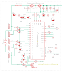
下面包含了我们的原理图。