请注意,本文内容源自机器翻译,可能存在语法或其它翻译错误,仅供参考。如需获取准确内容,请参阅链接中的英语原文或自行翻译。
器件型号:BQ76952 主题中讨论的其他器件: BQSTUDIO、BQ34Z100-G1
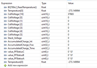
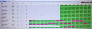
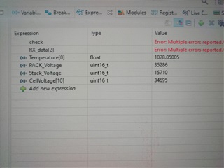
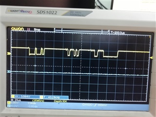
您好先生,长期以来我一直在尝试与 BQ76952和 STM32F103 viz. I2C 通信时,我还连接示波器观看 SDL 和 SCL 的图像 ,我也附加了图像,在设置相同的后,我总是变得不需要(在我的理解) 像这样的数据(例如单元读数、温度)。
7880mV
7880mV
7880mV
7880mV
10450mV
10450mV
10450mV
10450mV
10450mV
10450mV
7880mV
7880mV
7880mV
7880mV

,
/* USER CODE BEGIN Header */
/**
  ******************************************************************************
  * @file           : main.c
  * @brief          : Main program body
  ******************************************************************************
  * @attention
  *
  * <h2><center> Copyright (c) 2023 STMicroelectronics.
  * All rights reserved.</center></h2>
  *
  * This software component is licensed by ST under BSD 3-Clause license,
  * the "License"; You may not use this file except in compliance with the
  * License. You may obtain a copy of the License at:
  *                        opensource.org/licenses/BSD-3-Clause
  *
  ******************************************************************************
  */
/* USER CODE END Header */
/* Includes ------------------------------------------------------------------*/
#include "main.h"
#include <stdio.h>
/* Private includes ----------------------------------------------------------*/
/* USER CODE BEGIN Includes */

/* USER CODE END Includes */

/* Private typedef -----------------------------------------------------------*/
/* USER CODE BEGIN PTD */
#define DEV_ADDR  0x10  // BQ769x2 address is 0x10 including R/W bit or 0x8 as 7-bit address
#define CRC_Mode 0  // 0 for disabled, 1 for enabled
#define MAX_BUFFER_SIZE     10
/* USER CODE END PTD */

/* Private define ------------------------------------------------------------*/
/* USER CODE BEGIN PD */
/* USER CODE END PD */

/* Private macro -------------------------------------------------------------*/
/* USER CODE BEGIN PM */

/* USER CODE END PM */

/* Private variables ---------------------------------------------------------*/
I2C_HandleTypeDef hi2c1;

TIM_HandleTypeDef htim1;

UART_HandleTypeDef huart1;

/* USER CODE BEGIN PV */
uint8_t spiData [2];
uint8_t spiRxData [2];
uint8_t rxdata [2];
uint8_t busyData [2] = {0xFF, 0xFF};

uint8_t TX_2Byte [2] = {0x00, 0x00};
uint8_t TX_3Byte [3] = {0x00, 0x00, 0x00};
uint8_t TX_4Byte [4] = {0x00, 0x00, 0x00, 0x00};
uint8_t TX_Buffer [MAX_BUFFER_SIZE] = {0x00,0x00,0x00,0x00,0x00,0x00,0x00,0x00,0x00,0x00};

uint8_t RX_2Byte [2] = {0x00, 0x00};
uint8_t RX_3Byte [3] = {0x00, 0x00, 0x00};
uint8_t RX_4Byte [4] = {0x00, 0x00, 0x00, 0x00};
uint8_t RX_12Byte [12] = {0x00, 0x00, 0x00, 0x00, 0x00, 0x00, 0x00, 0x00, 0x00, 0x00, 0x00, 0x00};
uint8_t RX_Buffer [MAX_BUFFER_SIZE] = {0x00,0x00,0x00,0x00,0x00,0x00,0x00,0x00,0x00,0x00};
unsigned int RX_CRC_Check = 0;

// Variables for cell voltages, temperatures, CC2 current, Stack voltage, PACK Pin voltage, LD Pin voltage
uint16_t CellVoltage [16] = {0x00,0x00,0x00,0x00,0x00,0x00,0x00,0x00,0x00,0x00,0x00,0x00,0x00,0x00,0x00,0x00};
float Temperature [3] = {0,0,0};
float FET_Temperature = 0;
uint16_t Stack_Voltage = 0x00;
uint16_t LD_Voltage = 0x00;
uint16_t PACK_Voltage = 0x00;
uint16_t PACK_Current = 0x00;
uint16_t AlarmBits = 0x00;

uint8_t SafetyStatusA;  // Safety Status Register A
uint8_t SafetyStatusB;  // Safety Status Register B
uint8_t SafetyStatusC;  // Safety Status Register C
uint8_t PFStatusA;   // Permanent Fail Status Register A
uint8_t PFStatusB;   // Permanent Fail Status Register B
uint8_t PFStatusC;   // Permanent Fail Status Register C
uint8_t FET_Status;  // FET Status register contents See TRM Section 12.2.20  - Shows states of FETs

uint16_t CB_ActiveCells;  // Cell Balancing Active Cells
uint16_t DEVICE_NUMBER;

uint8_t	UV_Fault = 0;   // under-voltage fault state
uint8_t	OV_Fault = 0;   // over-voltage fault state
uint8_t	SCD_Fault = 0;  // short-circuit fault state
uint8_t	OCD_Fault = 0;  // over-current fault state
uint8_t LD_ON = 0;							// Load Detect status bit
uint8_t DCHG = 0;   // discharge FET state
uint8_t CHG = 0;   // charge FET state
uint8_t PCHG = 0;  // pre-charge FET state
uint8_t PDSG = 0;  // pre-discharge FET state

uint32_t AccumulatedCharge_Int;
uint32_t AccumulatedCharge_Frac;
uint32_t AccumulatedCharge_Time;
/* USER CODE END PV */

/* Private function prototypes -----------------------------------------------*/
void SystemClock_Config(void);
static void MX_GPIO_Init(void);
static void MX_I2C1_Init(void);
static void MX_TIM1_Init(void);
static void MX_USART1_UART_Init(void);
/* USER CODE BEGIN PFP */

/* USER CODE END PFP */

/* Private user code ---------------------------------------------------------*/
/* USER CODE BEGIN 0 */
void uprint(char * str)
{
	HAL_UART_Transmit(&huart1, (uint8_t*)str, strlen(str), 100);
}
/* USER CODE END 0 */
void delayUS(uint32_t us) {   // Sets the delay in microseconds.
	__HAL_TIM_SET_COUNTER(&htim1,0);  // set the counter value a 0
	while (__HAL_TIM_GET_COUNTER(&htim1) < us);  // wait for the counter to reach the us input in the parameter
}

void delay_ticks(uint32_t ticks)
{
    SysTick->LOAD = ticks;
    SysTick->VAL = 0;
    SysTick->CTRL = SysTick_CTRL_ENABLE_Msk;
    // COUNTFLAG is a bit that is set to 1 when counter reaches 0.
    // It's automatically cleared when read.
    while ((SysTick->CTRL & SysTick_CTRL_COUNTFLAG_Msk) == 0);
    SysTick->CTRL = 0;
}

void CopyArray(uint8_t *source, uint8_t *dest, uint8_t count)
{
    uint8_t copyIndex = 0;
    for (copyIndex = 0; copyIndex < count; copyIndex++)
    {
        dest[copyIndex] = source[copyIndex];
    }
}

unsigned char Checksum(unsigned char *ptr, unsigned char len)
	// Calculates the checksum when writing to a RAM register. The checksum is the inverse of the sum of the bytes.
{
	unsigned char i;
	unsigned char checksum = 0;

	for(i=0; i<len; i++)
		checksum += ptr[i];

	checksum = 0xff & ~checksum;

	return(checksum);
}


unsigned char CRC8(unsigned char *ptr, unsigned char len)
{
	unsigned char i;
	unsigned char crc=0;
	while(len--!=0)
	{
		for(i=0x80; i!=0; i/=2)
		{
			if((crc & 0x80) != 0)
			{
				crc *= 2;
				crc ^= 0x107;
			}
			else
				crc *= 2;

			if((*ptr & i)!=0)
				crc ^= 0x107;
		}
		ptr++;
	}
	return(crc);
}

void I2C_WriteReg(uint8_t reg_addr, uint8_t *reg_data, uint8_t count)
{
		#if CRC_Mode
		{
		uint8_t crc_count = 0;
		crc_count = count * 2;
		uint8_t crc1stByteBuffer [3] = {0x10, reg_addr, reg_data[0]};
		unsigned int j;
		unsigned int i;
		uint8_t temp_crc_buffer [3];

		TX_Buffer[0] = reg_data[0];
		TX_Buffer[1] = CRC8(crc1stByteBuffer,3);

		j = 2;
		for(i=1; i<count; i++)
		{
			TX_Buffer[j] = reg_data[i];
			j = j + 1;
			temp_crc_buffer[0] = reg_data[i];
			TX_Buffer[j] = CRC8(temp_crc_buffer,1);
			j = j + 1;
		}
		HAL_I2C_Mem_Write(&hi2c1, DEV_ADDR, reg_addr, 1, TX_Buffer, count, 1000);
		}
		#endif

		#if CRC_Mode < 1
			HAL_I2C_Mem_Write(&hi2c1, DEV_ADDR, reg_addr, 1, reg_data, count, 1000);
		#endif
}


int I2C_ReadReg(uint8_t reg_addr, uint8_t *reg_data, uint8_t count)
{
	unsigned int RX_CRC_Fail = 0;  // reset to 0. If in CRC Mode and CRC fails, this will be incremented.

	#if CRC_Mode
	{
		uint8_t crc_count = 0;
		uint8_t ReceiveBuffer [10] = {0x00,0x00,0x00,0x00,0x00,0x00,0x00,0x00,0x00,0x00};
		crc_count = count * 2;
		unsigned int j;
		unsigned int i;
		unsigned char CRCc = 0;
		uint8_t temp_crc_buffer [3];

		HAL_I2C_Mem_Read(&hi2c1, DEV_ADDR, reg_addr, 1, ReceiveBuffer, crc_count, 1000);
		uint8_t crc1stByteBuffer [4] = {0x10, reg_addr, 0x11, ReceiveBuffer[0]};
		CRCc = CRC8(crc1stByteBuffer,4);
		if (CRCc != ReceiveBuffer[1])
			RX_CRC_Fail += 1;

		RX_Buffer[0] = ReceiveBuffer[0];

		j = 2;
		for (i=1; i<count; i++)
		{
			RX_Buffer[i] = ReceiveBuffer[j];
			temp_crc_buffer[0] = ReceiveBuffer[j];
			j = j + 1;
			CRCc = CRC8(temp_crc_buffer,1);
			if (CRCc != ReceiveBuffer[j])
				RX_CRC_Fail += 1;
			j = j + 1;
		}
		CopyArray(RX_Buffer, reg_data, crc_count);
	}
	#endif

	#if CRC_Mode < 1
			HAL_I2C_Mem_Read(&hi2c1, DEV_ADDR, reg_addr, 1, reg_data, count, 1000);
	#endif

	  return 0;
}


void AFE_Reset() {
	// Reset command. Resets all registers to default values or the values programmed in OTP.
	TX_2Byte[0] = 0x12; TX_2Byte[1] = 0x00;
	I2C_WriteReg(0x3E,TX_2Byte,2);
}

void AFE_Init() {
	// Configures all parameters in device RAM

	// Enter CONFIGUPDATE mode (Subcommand 0x0090) - It is required to be in CONFIG_UPDATE mode to program the device RAM settings
	// See TRM Section 7.6 for full description of CONFIG_UPDATE mode
	TX_2Byte[0] = 0x90; TX_2Byte[1] = 0x00;
	I2C_WriteReg(0x3E,TX_2Byte,2);

	delayUS(2000);

	// After entering CONFIG_UPDATE mode, RAM registers can be programmed. When programming RAM, checksum and length must also be
	// programmed for the change to take effect. All of the RAM registers are described in detail in Chapter 13 of the BQ76952 TRM.
	// An easier way to find the descriptions is in the BQStudio Data Memory screen. When you move the mouse over the register name,
	// a full description of the register and the bits will pop up on the screen.
	// A summary of the Data Memory is also in Section 13.9 of the TRM.

	// 'Power Config' - Set DSLP_LDO  - 0x9234 = 0x2D82  (See TRM section 13.3.2)
	// Setting the DSLP_LDO bit allows the LDOs to remain active when the device goes into Deep Sleep mode
  TX_4Byte[0] = 0x34; TX_4Byte[1] = 0x92; TX_4Byte[2] = 0x82; TX_4Byte[3] = 0x2D;
  I2C_WriteReg(0x3E, TX_4Byte, 4);
	delayUS(1000);
	TX_2Byte[0] = Checksum(TX_4Byte, 4); TX_2Byte[1] = 0x06;  // Checksum and Length
  I2C_WriteReg(0x60, TX_2Byte, 2);
	delayUS(1000);

	// 'REG0 Config' - set REG0_EN bit to enable pre-regulator
	TX_3Byte[0] = 0x37; TX_3Byte[1] = 0x92; TX_3Byte[2] = 0x01;
  I2C_WriteReg(0x3E, TX_3Byte, 3);
	delayUS(1000);
	TX_2Byte[0] = Checksum(TX_3Byte, 3); TX_2Byte[1] = 0x05;
  I2C_WriteReg(0x60, TX_2Byte, 2);
	delayUS(1000);

	// 'REG12 Config' - Enable REG1 with 3.3V output
	TX_3Byte[0] = 0x36; TX_3Byte[1] = 0x92; TX_3Byte[2] = 0x0D;
  I2C_WriteReg(0x3E, TX_3Byte, 3);
	delayUS(1000);
	TX_2Byte[0] = Checksum(TX_3Byte, 3); TX_2Byte[1] = 0x05;
  I2C_WriteReg(0x60, TX_2Byte, 2);
	delayUS(1000);

	// 'VCell Mode' - Enable 16 cells - 0x9304 = 0x0000  (See TRM section 13.3.2.19)
	// 0x0000 sets the default value of 16 cells.
  TX_4Byte[0] = 0x04; TX_4Byte[1] = 0x93; TX_4Byte[2] = 0x00; TX_4Byte[3] = 0x00;
  I2C_WriteReg(0x3E, TX_4Byte, 4);
	delayUS(1000);
	TX_2Byte[0] = Checksum(TX_4Byte, 4); TX_2Byte[1] = 0x06;  // Checksum and Length
  I2C_WriteReg(0x60, TX_2Byte, 2);
	delayUS(1000);

	// 'Default Alarm Mask' - Enable FullScan and ADScan bits
	// 0xF882
  TX_4Byte[0] = 0x6D; TX_4Byte[1] = 0x92; TX_4Byte[2] = 0x82; TX_4Byte[3] = 0xF8;
  I2C_WriteReg(0x3E, TX_4Byte, 4);
	delayUS(1000);
	TX_2Byte[0] = Checksum(TX_4Byte, 4); TX_2Byte[1] = 0x06;  // Checksum and Length
  I2C_WriteReg(0x60, TX_2Byte, 2);
	delayUS(1000);

	// Enable protections in 'Enabled Protections A' 0x9261 = 0xBC (See TRM section 13.3.3.2)
	// Enables SCD (short-circuit), OCD1 (over-current in discharge), OCC (over-current in charge),
	// COV (over-voltage), CUV (under-voltage)
	TX_3Byte[0] = 0x61; TX_3Byte[1] = 0x92; TX_3Byte[2] = 0xFC;
  I2C_WriteReg(0x3E, TX_3Byte, 3);
	delayUS(1000);
	TX_2Byte[0] = Checksum(TX_3Byte, 3); TX_2Byte[1] = 0x05;
  I2C_WriteReg(0x60, TX_2Byte, 2);
	delayUS(1000);

	// Enable all protections in 'Enabled Protections B' 0x9262 = 0xF7 (See TRM section 13.3.3.3)
	// Enables OTF (over-temperature FET), OTINT (internal over-temperature), OTD (over-temperature in discharge),
	// OTC (over-temperature in charge), UTINT (internal under-temperature), UTD (under-temperature in discharge), UTC (under-temperature in charge)
	TX_3Byte[0] = 0x62; TX_3Byte[1] = 0x92; TX_3Byte[2] = 0xF7;
  I2C_WriteReg(0x3E, TX_3Byte, 3);
	delayUS(1000);
	TX_2Byte[0] = Checksum(TX_3Byte, 3); TX_2Byte[1] = 0x05;
  I2C_WriteReg(0x60, TX_2Byte, 2);
	delayUS(1000);

	// Set TS1 to measure Cell Temperature - 0x92FD = 0x07   (See TRM Section 13.3.2.12)
	TX_3Byte[0] = 0xFD; TX_3Byte[1] = 0x92; TX_3Byte[2] = 0x07;
  I2C_WriteReg(0x3E, TX_3Byte, 3);
	delayUS(1000);
	TX_2Byte[0] = Checksum(TX_3Byte, 3); TX_2Byte[1] = 0x05;
  I2C_WriteReg(0x60, TX_2Byte, 2);
	delayUS(1000);

	// Set TS3 to measure FET Temperature - 0x92FF = 0x0F   (See TRM Section 13.3.2.14)
	TX_3Byte[0] = 0xFF; TX_3Byte[1] = 0x92; TX_3Byte[2] = 0x0F;
  I2C_WriteReg(0x3E, TX_3Byte, 3);
	delayUS(1000);
	TX_2Byte[0] = Checksum(TX_3Byte, 3); TX_2Byte[1] = 0x05;
  I2C_WriteReg(0x60, TX_2Byte, 2);
	delayUS(1000);

	// Set DFETOFF pin to control BOTH CHG and DSG FET - 0x92FB = 0x42 (set to 0x00 to disable)
	// See TRM section 13.3.2.10, Table 13-7
	TX_3Byte[0] = 0xFB; TX_3Byte[1] = 0x92; TX_3Byte[2] = 0x42;
  I2C_WriteReg(0x3E, TX_3Byte, 3);
	delayUS(1000);
	TX_2Byte[0] = Checksum(TX_3Byte, 3); TX_2Byte[1] = 0x05;
  I2C_WriteReg(0x60, TX_2Byte, 2);
	delayUS(1000);

	// Set up Alert Pin - 0x92FC = 0x2A  - See TRM Section 13.3.2.11, Table 13-8
	// This configures the Alert pin to drive high (REG1 voltage) when enabled.
	// Other options available include active-low, drive HiZ, drive using REG18 (1.8V), weak internal pull-up and pull-down
	TX_3Byte[0] = 0xFC; TX_3Byte[1] = 0x92; TX_3Byte[2] = 0x2A;
  I2C_WriteReg(0x3E, TX_3Byte, 3);
	delayUS(1000);
	TX_2Byte[0] = Checksum(TX_3Byte, 3); TX_2Byte[1] = 0x05;
  I2C_WriteReg(0x60, TX_2Byte, 2);
	delayUS(1000);


	// Set up Cell Balancing Configuration - 0x9335 = 0x03   -  Automated balancing while in Relax or Charge modes
	// See TRM Section 13.3.11. Chapter 10 of TRM describes Cell Balancing in detail
	// Also see "Cell Balancing with BQ76952, BQ76942 Battery Monitors" document on ti.com
	TX_3Byte[0] = 0x35; TX_3Byte[1] = 0x93; TX_3Byte[2] = 0x03;
  I2C_WriteReg(0x3E, TX_3Byte, 3);
	delayUS(1000);
	TX_2Byte[0] = Checksum(TX_3Byte, 3); TX_2Byte[1] = 0x05;
  I2C_WriteReg(0x60, TX_2Byte, 2);
	delayUS(1000);

	// Set up COV (over-voltage) Threshold - 0x9278 = 0x55 (4301 mV)
	// COV Threshold is this value multiplied by 50.6mV  See TRM section 13.6.2
	TX_3Byte[0] = 0x78; TX_3Byte[1] = 0x92; TX_3Byte[2] = 0x55;
  I2C_WriteReg(0x3E, TX_3Byte, 3);
	delayUS(1000);
	TX_2Byte[0] = Checksum(TX_3Byte, 3); TX_2Byte[1] = 0x05;
  I2C_WriteReg(0x60, TX_2Byte, 2);
	delayUS(1000);

	// Set up SCD Threshold - 0x9286 = 0x05 (100 mV = 100A across 1mOhm sense resistor)
	// See TRM section 13.6.7    0x05=100mV
	TX_3Byte[0] = 0x86; TX_3Byte[1] = 0x92; TX_3Byte[2] = 0x05;
  I2C_WriteReg(0x3E, TX_3Byte, 3);
	delayUS(1000);
	TX_2Byte[0] = Checksum(TX_3Byte, 3); TX_2Byte[1] = 0x05;
  I2C_WriteReg(0x60, TX_2Byte, 2);
	delayUS(1000);

	// Set up SCD Delay - 0x9287 = 0x03 (30 us)    See TRM section 13.6.7
	// Units of 15us
	TX_3Byte[0] = 0x87; TX_3Byte[1] = 0x92; TX_3Byte[2] = 0x03;
  I2C_WriteReg(0x3E, TX_3Byte, 3);
	delayUS(1000);
	TX_2Byte[0] = Checksum(TX_3Byte, 3); TX_2Byte[1] = 0x05;
  I2C_WriteReg(0x60, TX_2Byte, 2);
	delayUS(1000);

	// Set up SCDL Latch Limit to 1 to set SCD recovery only with load removal 0x9295 = 0x01
	// If this is not set, then SCD will recover based on time (SCD Recovery Time parameter).
	// See TRM section 13.6.11.1
	TX_3Byte[0] = 0x95; TX_3Byte[1] = 0x92; TX_3Byte[2] = 0x01;
  I2C_WriteReg(0x3E, TX_3Byte, 3);
	delayUS(1000);
	TX_2Byte[0] = Checksum(TX_3Byte, 3); TX_2Byte[1] = 0x05;
  I2C_WriteReg(0x60, TX_2Byte, 2);
	delayUS(1000);


	// Exit CONFIGUPDATE mode  - Subcommand 0x0092
	TX_2Byte[0] = 0x92; TX_2Byte[1] = 0x00;
	I2C_WriteReg(0x3E,TX_2Byte,2);
	delayUS(1000);
}

//  ********************************* FET Control Commands  ***************************************

void AFE_FET_ENABLE() {
	// Toggles the FET_EN bit in the Manufacturing Status register. So this command can be used to enable or disable the FETs.
	TX_2Byte[0] = 0x22; TX_2Byte[1] = 0x00;
	I2C_WriteReg(0x3E,TX_2Byte,2);
}

void AFE_FET_Control(uint8_t FET_states) {  // Bit3 = PCHG_OFF, Bit 2 = CHG_OFF, Bit1 = PDSG_OFF, Bit 0 = DSG_OFF
	TX_3Byte[0] = 0x97; TX_3Byte[1] = 0x00; TX_3Byte[2] = FET_states;
	I2C_WriteReg(0x3E,TX_3Byte,3);
	delayUS(1000);
	TX_2Byte[0] = Checksum(TX_3Byte, 3); TX_2Byte[1] = 0x05;
  I2C_WriteReg(0x60, TX_2Byte, 2);
}

void DSG_PDSG_OFF() {
	// Disable discharge (and pre-discharge) FETs
	// Subcommand 0x0093  See TRM Table 5-8  (DSG_PDSG_OFF())
	TX_2Byte[0] = 0x93; TX_2Byte[1] = 0x00;
	I2C_WriteReg(0x3E,TX_2Byte,2);
}

void CHG_PCHG_OFF() {
	// Disable charge (and pre-charge) FETs
	// Subcommand 0x0094  See TRM Table 5-8  (CHG_PCHG_OFF())
	TX_2Byte[0] = 0x94; TX_2Byte[1] = 0x00;
	I2C_WriteReg(0x3E,TX_2Byte,2);
}

void AFE_ALL_FETS_OFF() {
	// Disable all FETs with command 0x0095  See TRM Table 5-8
	TX_2Byte[0] = 0x95; TX_2Byte[1] = 0x00;
	I2C_WriteReg(0x3E,TX_2Byte,2);
}

void AFE_ALL_FETS_ON() {
	// All all FETs to be enabled with command 0x0096  See TRM Table 5-8
	TX_2Byte[0] = 0x96; TX_2Byte[1] = 0x00;
	I2C_WriteReg(0x3E,TX_2Byte,2);
}

void AFE_BOTHOFF () {
	// Disables all FETs using the DFETOFF (BOTHOFF) pin
	HAL_GPIO_WritePin(GPIOA, GPIO_PIN_8, GPIO_PIN_SET);  // DFETOFF pin (BOTHOFF) set low
}

void AFE_RESET_BOTHOFF () {
	// Resets DFETOFF (BOTHOFF) pin
	HAL_GPIO_WritePin(GPIOA, GPIO_PIN_8, GPIO_PIN_RESET);  // DFETOFF pin (BOTHOFF) set low
}

void AFE_ReadFETStatus() {
	// Read FET Status to see which FETs are enabled
	I2C_ReadReg(0x7F, RX_2Byte, 2);
  FET_Status = (RX_2Byte[1]*256 + RX_2Byte[0]);
	DCHG = 0x4 & RX_2Byte[0];   // discharge FET state
	CHG = 0x1 & RX_2Byte[0];   // charge FET state
	PCHG = 0x2 & RX_2Byte[0];  // pre-charge FET state
	PDSG = 0x8 & RX_2Byte[0];  // pre-discharge FET state
}


// ********************************* End of FET Control Commands *********************************


// ********************************* AFE Cell Balancing Commands   *****************************************

void CB_ACTIVE_CELLS() {
	// Check status of which cells are balancing
	TX_2Byte[0] = 0x83; TX_2Byte[1] = 0x00;
	I2C_WriteReg(0x3E,TX_2Byte,2);
	I2C_ReadReg(0x40, RX_2Byte, 2);
  CB_ActiveCells = (RX_2Byte[1]*256 + RX_2Byte[0]);
}


// ********************************* End of AFE Cell Balancing Commands   *****************************************


// ********************************* AFE Power Commands   *****************************************
void AFE_DeepSleep() {
	// Puts the device into DEEPSLEEP mode. See TRM section 7.4
	TX_2Byte[0] = 0x0F; TX_2Byte[1] = 0x00;
	I2C_WriteReg(0x3E,TX_2Byte,2);
	I2C_WriteReg(0x3E,TX_2Byte,2);
}

void AFE_ExitDeepSleep() {
	// Exits DEEPSLEEP mode. See TRM section 7.4
	TX_2Byte[0] = 0x0E; TX_2Byte[1] = 0x00;
	I2C_WriteReg(0x3E,TX_2Byte,2);
}

void AFE_ShutdownCommand() {
	// Puts the device into SHUTDOWN mode. See TRM section 7.5
	TX_2Byte[0] = 0x10; TX_2Byte[1] = 0x00;
	I2C_WriteReg(0x3E,TX_2Byte,2);
}

void AFE_ShutdownPin() {
	// Puts the device into SHUTDOWN mode using the RST_SHUT pin
	HAL_GPIO_WritePin(GPIOA, GPIO_PIN_9, GPIO_PIN_SET);  // Sets RST_SHUT pin
}

void AFE_ReleaseShutdownPin() {
	// Releases the RST_SHUT pin
	HAL_GPIO_WritePin(GPIOA, GPIO_PIN_9, GPIO_PIN_RESET);  // Resets RST_SHUT pin
}

void AFE_SLEEP_ENABLE() { // SLEEP_ENABLE 0x0099
	// Allows the device to enter Sleep mode if current is below Sleep Current. See TRM section 7.3
	TX_2Byte[0] = 0x99; TX_2Byte[1] = 0x00;
	I2C_WriteReg(0x3E,TX_2Byte,2);
}

void AFE_SLEEP_DISABLE() { // SLEEP_DISABLE 0x009A
	// Takes the device out of sleep mode. See TRM section 7.3
	TX_2Byte[0] = 0x9A; TX_2Byte[1] = 0x00;
	I2C_WriteReg(0x3E,TX_2Byte,2);
}

// ********************************* End of AFE Power Commands   *****************************************


// ********************************* AFE Status and Fault Commands   *****************************************

uint16_t AFE_ReadAlarmStatus() {
	// Read this register to find out why the Alert pin was asserted. See section 6.6 of the TRM for full description.
	I2C_ReadReg(0x62, RX_2Byte, 2);
	return (RX_2Byte[1]*256 + RX_2Byte[0]);
}

void AFE_ReadSafetyStatus() {
	// Read Safety Status A/B/C and find which bits are set
	// This shows which primary protections have been triggered
	I2C_ReadReg(0x03, RX_2Byte, 2);
	SafetyStatusA = (RX_2Byte[1]*256 + RX_2Byte[0]);
	UV_Fault = 0x4 & RX_2Byte[0];
	OV_Fault = 0x8 & RX_2Byte[0];
	SCD_Fault = 0x8 & RX_2Byte[1];
	OCD_Fault = 0x2 & RX_2Byte[1];
	I2C_ReadReg(0x05, RX_2Byte, 2);
	SafetyStatusB = (RX_2Byte[1]*256 + RX_2Byte[0]);
	I2C_ReadReg(0x07, RX_2Byte, 2);
	SafetyStatusC = (RX_2Byte[1]*256 + RX_2Byte[0]);
}

void AFE_ReadPFStatus() {
	// Read Permanent Fail Status A/B/C and find which bits are set
	// This shows which permanent failures have been triggered
	I2C_ReadReg(0x0B, RX_2Byte, 2);
	PFStatusA = (RX_2Byte[1]*256 + RX_2Byte[0]);
	I2C_ReadReg(0x0D, RX_2Byte, 2);
	PFStatusB = (RX_2Byte[1]*256 + RX_2Byte[0]);
	I2C_ReadReg(0x0F, RX_2Byte, 2);
	PFStatusC = (RX_2Byte[1]*256 + RX_2Byte[0]);
}


void AFE_ControlStatus() {
	// Control status register - Bit0 - LD_ON (load detected)
	// See TRM Table 6-1
	I2C_ReadReg(0x00, RX_2Byte, 2);
  LD_ON = 0x1 & RX_2Byte[0];
}

void AFE_BatteryStatus() {
	// Battery status register - See TRM Table 6-2
	I2C_ReadReg(0x12, RX_2Byte, 2);
}

void AFE_ClearFaults() {
	TX_2Byte[0] = 0x00; TX_2Byte[1] = 0xF8;
	I2C_WriteReg(0x62,TX_2Byte,2);
}

void AFE_ClearScanBits() {
	TX_2Byte[0] = 0x82; TX_2Byte[1] = 0x00;
	I2C_WriteReg(0x62,TX_2Byte,2);
}

void AFE_PFReset() {
	TX_2Byte[0] = 0x29; TX_2Byte[1] = 0x00;
	I2C_WriteReg(0x3E,TX_2Byte,2);
}

uint16_t AFE_DeviceID() {
	// Read Device ID using Subcommand 0x0001
	TX_2Byte[0] = 0x01; TX_2Byte[1] = 0x00;
	I2C_WriteReg(0x3E,TX_2Byte,2);
	delayUS(500);
	I2C_ReadReg(0x40, RX_2Byte, 2);
	return (RX_2Byte[1]*256 + RX_2Byte[0]);
}
// ********************************* End of AFE Status and Fault Commands   *****************************************


// ********************************* AFE Measurement Commands   *****************************************

uint16_t AFE_ReadCellVoltage(uint8_t channel) {
	I2C_ReadReg(channel*2+0x12, RX_2Byte, 2);
	return (RX_2Byte[1]*256 + RX_2Byte[0]);     // cell voltage is reported in mV
}

uint16_t AFE_ReadStackVoltage() {
	I2C_ReadReg(0x34, RX_2Byte, 2);
	return 10 * (RX_2Byte[1]*256 + RX_2Byte[0]);  // voltage is reported in 0.01V units
}

uint16_t AFE_ReadPackVoltage() {
	I2C_ReadReg(0x36, RX_2Byte, 2);
	return 10 * (RX_2Byte[1]*256 + RX_2Byte[0]);  // voltage is reported in 0.01V units
}

uint16_t AFE_ReadLDVoltage() {
	I2C_ReadReg(0x38, RX_2Byte, 2);
	return 10 * (RX_2Byte[1]*256 + RX_2Byte[0]);  // voltage is reported in 0.01V units
}

uint16_t AFE_ReadCurrent() {
	I2C_ReadReg(0x3A, RX_2Byte, 2);
	return (RX_2Byte[1]*256 + RX_2Byte[0]);  // current is reported in mA
}


float AFE_ReadTemperature(uint8_t channel) {
	switch(channel)
	{
		case 0:
			I2C_ReadReg(0x70, RX_2Byte, 2);  // TS1 pin
			break;
		case 1:
			I2C_ReadReg(0x74, RX_2Byte, 2);  // TS3 pin, FET temperature
			break;
		default: break;
	}
	return (0.1 * (float)(RX_2Byte[1]*256 + RX_2Byte[0])) - 273.15;  // convert from 0.1K to Celcius
}


void AFE_ReadPassQ() {
	// Read Accumulated Charge and Time from DASTATUS6 (See TRM Table 4-6)
	TX_2Byte[0] = 0x76; TX_2Byte[1] = 0x00;
	I2C_WriteReg(0x3E,TX_2Byte,2);
	delayUS(1000);
	I2C_ReadReg(0x40, RX_12Byte, 12);
	AccumulatedCharge_Int = ((RX_12Byte[3]<<24) + (RX_12Byte[2]<<16) + (RX_12Byte[1]<<8) + RX_12Byte[0]);
	AccumulatedCharge_Frac = ((RX_12Byte[7]<<24) + (RX_12Byte[6]<<16) + (RX_12Byte[5]<<8) + RX_12Byte[4]);
	AccumulatedCharge_Time = ((RX_12Byte[11]<<24) + (RX_12Byte[10]<<16) + (RX_12Byte[9]<<8) + RX_12Byte[8]);
}

void AFE_ClearPassQ() {
	// Clear Accumulated Charge and Time, command 0x0082
	TX_2Byte[0] = 0x82; TX_2Byte[1] = 0x00;
	I2C_WriteReg(0x3E,TX_2Byte,2);
}

// *********************************
/* USER CODE END 0 */

/**
  * @brief  The application entry point.
  * @retval int
  */
int main(void)
{
  /* USER CODE BEGIN 1 */
	uint8_t	I2C_Return;
  /* USER CODE END 1 */
	volatile int i = 0;
	char uart_buf[50];
	int uart_buf_len;
  /* USER CODE END 1 */
	uint16_t CellVoltage1 =0;
  /* MCU Configuration--------------------------------------------------------*/

  /* Reset of all peripherals, Initializes the Flash interface and the Systick. */
  HAL_Init();

  /* USER CODE BEGIN Init */

  /* USER CODE END Init */

  /* Configure the system clock */
  SystemClock_Config();

  /* USER CODE BEGIN SysInit */

  /* USER CODE END SysInit */

  /* Initialize all configured peripherals */
  MX_GPIO_Init();
  MX_I2C1_Init();
  MX_TIM1_Init();
  MX_USART1_UART_Init();
  /* USER CODE BEGIN 2 */
  HAL_TIM_Base_Start(&htim1);

  	HAL_GPIO_WritePin(GPIOA, GPIO_PIN_9, GPIO_PIN_RESET);  // RST_SHUT pin set low
  	HAL_GPIO_WritePin(GPIOA, GPIO_PIN_8, GPIO_PIN_RESET);  // DFETOFF pin (BOTHOFF) set low
      delayUS(10000);


  	AFE_Reset();
  	delayUS(60000);
  	AFE_Init();
  	delayUS(10000);
  	AFE_FET_ENABLE();
  	delayUS(10000);

  	AFE_SLEEP_DISABLE();

  	delayUS(60000); delayUS(60000); delayUS(60000); delayUS(60000);  //wait to start measurements after FETs close
  	CellVoltage[1] = AFE_ReadCellVoltage(1);
  	CellVoltage[5] = AFE_ReadCellVoltage(5);
  	CellVoltage[10] = AFE_ReadCellVoltage(10);
  	Stack_Voltage = AFE_ReadStackVoltage();
  	PACK_Voltage = AFE_ReadPackVoltage();
  	LD_Voltage = AFE_ReadLDVoltage();
  	PACK_Current = AFE_ReadCurrent();
  	Temperature[0] = AFE_ReadTemperature(0)m   ;
  	FET_Temperature = AFE_ReadTemperature(1);
  /* USER CODE END 2 */

  /* Infinite loop */
  /* USER CODE BEGIN WHILE */
  while (1)
  {
	  CellVoltage1 =0;
    /* USER CODE END WHILE */
	  CellVoltage1 = AFE_ReadCellVoltage(1);
	  Stack_Voltage = AFE_ReadStackVoltage();
	//Debug code - prints the Cell1 Voltage to a terminal window
	uart_buf_len = sprintf(uart_buf, "%u mV\r\n", Temperature[1] );
	HAL_UART_Transmit(&huart1, (uint8_t *)uart_buf, uart_buf_len, 100);
	CellVoltage1 =0;
	CellVoltage[2] = AFE_ReadCellVoltage(2);

	CellVoltage[3] = AFE_ReadCellVoltage(3);
	CellVoltage[4] = AFE_ReadCellVoltage(4);
	CellVoltage[5] = AFE_ReadCellVoltage(5);
	CellVoltage[6] = AFE_ReadCellVoltage(6);
	CellVoltage[7] = AFE_ReadCellVoltage(7);
	CellVoltage[8] = AFE_ReadCellVoltage(8);
	CellVoltage[9] = AFE_ReadCellVoltage(9);
	CellVoltage[10] = AFE_ReadCellVoltage(10);
	//Stack_Voltage = AFE_ReadStackVoltage();
	PACK_Voltage = AFE_ReadPackVoltage();
	LD_Voltage = AFE_ReadLDVoltage();
	PACK_Current = AFE_ReadCurrent();
	Temperature[0] = AFE_ReadTemperature(2);
	FET_Temperature = AFE_ReadTemperature(1);

	AlarmBits = AFE_ReadAlarmStatus();
	//Debug code - prints the Cell1 Voltage to a terminal window
	// 		uart_buf_len = sprintf(uart_buf, "%u \r\n", AlarmBits);
	//	HAL_UART_Transmit(&huart1, (uint8_t *)uart_buf, uart_buf_len, 100);

	if (AlarmBits & 0x82) {
		AFE_ClearScanBits();
	}

	if (AlarmBits & 0xC000) {
		AFE_ReadSafetyStatus();
		AFE_ReadPFStatus();
		AFE_ClearFaults();
		AFE_PFReset();
	}
	CellVoltage1 =0;
	HAL_Delay(500);
    /* USER CODE BEGIN 3 */
  }
  /* USER CODE END 3 */
}

/**
  * @brief System Clock Configuration
  * @retval None
  */
void SystemClock_Config(void)
{
  RCC_OscInitTypeDef RCC_OscInitStruct = {0};
  RCC_ClkInitTypeDef RCC_ClkInitStruct = {0};

  /** Initializes the RCC Oscillators according to the specified parameters
  * in the RCC_OscInitTypeDef structure.
  */
  RCC_OscInitStruct.OscillatorType = RCC_OSCILLATORTYPE_HSE;
  RCC_OscInitStruct.HSEState = RCC_HSE_ON;
  RCC_OscInitStruct.HSEPredivValue = RCC_HSE_PREDIV_DIV1;
  RCC_OscInitStruct.HSIState = RCC_HSI_ON;
  RCC_OscInitStruct.PLL.PLLState = RCC_PLL_ON;
  RCC_OscInitStruct.PLL.PLLSource = RCC_PLLSOURCE_HSE;
  RCC_OscInitStruct.PLL.PLLMUL = RCC_PLL_MUL8;
  if (HAL_RCC_OscConfig(&RCC_OscInitStruct) != HAL_OK)
  {
    Error_Handler();
  }
  /** Initializes the CPU, AHB and APB buses clocks
  */
  RCC_ClkInitStruct.ClockType = RCC_CLOCKTYPE_HCLK|RCC_CLOCKTYPE_SYSCLK
                              |RCC_CLOCKTYPE_PCLK1|RCC_CLOCKTYPE_PCLK2;
  RCC_ClkInitStruct.SYSCLKSource = RCC_SYSCLKSOURCE_PLLCLK;
  RCC_ClkInitStruct.AHBCLKDivider = RCC_SYSCLK_DIV1;
  RCC_ClkInitStruct.APB1CLKDivider = RCC_HCLK_DIV2;
  RCC_ClkInitStruct.APB2CLKDivider = RCC_HCLK_DIV1;

  if (HAL_RCC_ClockConfig(&RCC_ClkInitStruct, FLASH_LATENCY_2) != HAL_OK)
  {
    Error_Handler();
  }
}

/**
  * @brief I2C1 Initialization Function
  * @param None
  * @retval None
  */
static void MX_I2C1_Init(void)
{


	  /* USER CODE BEGIN I2C1_Init 0 */

	  /* USER CODE END I2C1_Init 0 */

	  /* USER CODE BEGIN I2C1_Init 1 */

	  /* USER CODE END I2C1_Init 1 */
	  hi2c1.Instance = I2C1;
	  hi2c1.Init.ClockSpeed = 400000;
	  hi2c1.Init.DutyCycle = I2C_DUTYCYCLE_2;
	  hi2c1.Init.OwnAddress1 = 0;
	  hi2c1.Init.AddressingMode = I2C_ADDRESSINGMODE_7BIT;
	  hi2c1.Init.DualAddressMode = I2C_DUALADDRESS_DISABLE;
	  hi2c1.Init.OwnAddress2 = 0;
	  hi2c1.Init.GeneralCallMode = I2C_GENERALCALL_DISABLE;
	  hi2c1.Init.NoStretchMode = I2C_NOSTRETCH_DISABLE;
	  if (HAL_I2C_Init(&hi2c1) != HAL_OK)
	  {
	    Error_Handler();
	  }
	  /* USER CODE BEGIN I2C1_Init 2 */

	  /* USER CODE END I2C1_Init 2 */

}

/**
  * @brief TIM1 Initialization Function
  * @param None
  * @retval None
  */
static void MX_TIM1_Init(void)
{

  /* USER CODE BEGIN TIM1_Init 0 */

  /* USER CODE END TIM1_Init 0 */

  TIM_ClockConfigTypeDef sClockSourceConfig = {0};
  TIM_MasterConfigTypeDef sMasterConfig = {0};

  /* USER CODE BEGIN TIM1_Init 1 */

  /* USER CODE END TIM1_Init 1 */
  htim1.Instance = TIM1;
  htim1.Init.Prescaler = 63;
  htim1.Init.CounterMode = TIM_COUNTERMODE_UP;
  htim1.Init.Period = 65535;
  htim1.Init.ClockDivision = TIM_CLOCKDIVISION_DIV1;
  htim1.Init.RepetitionCounter = 0;
  htim1.Init.AutoReloadPreload = TIM_AUTORELOAD_PRELOAD_DISABLE;
  if (HAL_TIM_Base_Init(&htim1) != HAL_OK)
  {
    Error_Handler();
  }
  sClockSourceConfig.ClockSource = TIM_CLOCKSOURCE_INTERNAL;
  if (HAL_TIM_ConfigClockSource(&htim1, &sClockSourceConfig) != HAL_OK)
  {
    Error_Handler();
  }
  sMasterConfig.MasterOutputTrigger = TIM_TRGO_RESET;
  sMasterConfig.MasterSlaveMode = TIM_MASTERSLAVEMODE_DISABLE;
  if (HAL_TIMEx_MasterConfigSynchronization(&htim1, &sMasterConfig) != HAL_OK)
  {
    Error_Handler();
  }
  /* USER CODE BEGIN TIM1_Init 2 */

  /* USER CODE END TIM1_Init 2 */

}

/**
  * @brief USART1 Initialization Function
  * @param None
  * @retval None
  */
static void MX_USART1_UART_Init(void)
{

  /* USER CODE BEGIN USART1_Init 0 */

  /* USER CODE END USART1_Init 0 */

  /* USER CODE BEGIN USART1_Init 1 */

  /* USER CODE END USART1_Init 1 */
  huart1.Instance = USART1;
  huart1.Init.BaudRate = 115200;
  huart1.Init.WordLength = UART_WORDLENGTH_8B;
  huart1.Init.StopBits = UART_STOPBITS_1;
  huart1.Init.Parity = UART_PARITY_NONE;
  huart1.Init.Mode = UART_MODE_TX_RX;
  huart1.Init.HwFlowCtl = UART_HWCONTROL_NONE;
  huart1.Init.OverSampling = UART_OVERSAMPLING_16;
  if (HAL_UART_Init(&huart1) != HAL_OK)
  {
    Error_Handler();
  }
  /* USER CODE BEGIN USART1_Init 2 */

  /* USER CODE END USART1_Init 2 */

}

/**
  * @brief GPIO Initialization Function
  * @param None
  * @retval None
  */
static void MX_GPIO_Init(void)
{
  GPIO_InitTypeDef GPIO_InitStruct = {0};

  /* GPIO Ports Clock Enable */
  __HAL_RCC_GPIOC_CLK_ENABLE();
  __HAL_RCC_GPIOD_CLK_ENABLE();
  __HAL_RCC_GPIOA_CLK_ENABLE();
  __HAL_RCC_GPIOB_CLK_ENABLE();

  /*Configure GPIO pin Output Level */
  HAL_GPIO_WritePin(GPIOC, GPIO_PIN_13, GPIO_PIN_RESET);

  /*Configure GPIO pin : PC13 */
  GPIO_InitStruct.Pin = GPIO_PIN_13;
  GPIO_InitStruct.Mode = GPIO_MODE_OUTPUT_PP;
  GPIO_InitStruct.Pull = GPIO_NOPULL;
  GPIO_InitStruct.Speed = GPIO_SPEED_FREQ_LOW;
  HAL_GPIO_Init(GPIOC, &GPIO_InitStruct);

}

/* USER CODE BEGIN 4 */

/* USER CODE END 4 */
void HAL_GPIO_EXTI_Callback ( uint16_t GPIO_Pin )
{
	if ( GPIO_Pin == GPIO_PIN_3 ) {
		HAL_GPIO_TogglePin (GPIOA, GPIO_PIN_5 );
	}
	else {
		__NOP ();
	}
}
/**
  * @brief  This function is executed in case of error occurrence.
  * @retval None
  */
void Error_Handler(void)
{
  /* USER CODE BEGIN Error_Handler_Debug */
  /* User can add his own implementation to report the HAL error return state */
  __disable_irq();
  while (1)
  {
  }
  /* USER CODE END Error_Handler_Debug */
}

#ifdef  USE_FULL_ASSERT
/**
  * @brief  Reports the name of the source file and the source line number
  *         where the assert_param error has occurred.
  * @param  file: pointer to the source file name
  * @param  line: assert_param error line source number
  * @retval None
  */
void assert_failed(uint8_t *file, uint32_t line)
{
  /* USER CODE BEGIN 6 */
  /* User can add his own implementation to report the file name and line number,
     ex: printf("Wrong parameters value: file %s on line %d\r\n", file, line) */
  /* USER CODE END 6 */
}
#endif /* USE_FULL_ASSERT */

/************************ (C) COPYRIGHT STMicroelectronics *****END OF FILE****/
Copyright (c) 2023 STMicroelectronics.
* All rights reserved.</center></h2>
*
* This software component is licensed by ST under BSD 3-Clause license,
* the "License"; You may not use this file except in compliance with the
* License. You may obtain a copy of the License at:
* opensource.org/licenses/BSD-3-Clause
*
******************************************************************************
*/
/* USER CODE END Header */
/* Includes ------------------------------------------------------------------*/
#include "main.h"
#include <stdio.h>
/* Private includes ----------------------------------------------------------*/
/* USER CODE BEGIN Includes */
/* USER CODE END Includes */
/* Private typedef -----------------------------------------------------------*/
/* USER CODE BEGIN PTD */
#define DEV_ADDR 0x10 // BQ769x2 address is 0x10 including R/W bit or 0x8 as 7-bit address
#define CRC_Mode 0 // 0 for disabled, 1 for enabled
#define MAX_BUFFER_SIZE 10
/* USER CODE END PTD */
/* Private define ------------------------------------------------------------*/
/* USER CODE BEGIN PD */
/* USER CODE END PD */
/* Private macro -------------------------------------------------------------*/
/* USER CODE BEGIN PM */
/* USER CODE END PM */
/* Private variables ---------------------------------------------------------*/
I2C_HandleTypeDef hi2c1;
TIM_HandleTypeDef htim1;
UART_HandleTypeDef huart1;
/* USER CODE BEGIN PV */
uint8_t spiData [2];
uint8_t spiRxData [2];
uint8_t rxdata [2];
uint8_t busyData [2] = {0xFF, 0xFF};
uint8_t TX_2Byte [2] = {0x00, 0x00};
uint8_t TX_3Byte [3] = {0x00, 0x00, 0x00};
uint8_t TX_4Byte [4] = {0x00, 0x00, 0x00, 0x00};
uint8_t TX_Buffer [MAX_BUFFER_SIZE] = {0x00,0x00,0x00,0x00,0x00,0x00,0x00,0x00,0x00,0x00};
uint8_t RX_2Byte [2] = {0x00, 0x00};
uint8_t RX_3Byte [3] = {0x00, 0x00, 0x00};
uint8_t RX_4Byte [4] = {0x00, 0x00, 0x00, 0x00};
uint8_t RX_12Byte [12] = {0x00, 0x00, 0x00, 0x00, 0x00, 0x00, 0x00, 0x00, 0x00, 0x00, 0x00, 0x00};
uint8_t RX_Buffer [MAX_BUFFER_SIZE] = {0x00,0x00,0x00,0x00,0x00,0x00,0x00,0x00,0x00,0x00};
unsigned int RX_CRC_Check = 0;
// Variables for cell voltages, temperatures, CC2 current, Stack voltage, PACK Pin voltage, LD Pin voltage
uint16_t CellVoltage [16] = {0x00,0x00,0x00,0x00,0x00,0x00,0x00,0x00,0x00,0x00,0x00,0x00,0x00,0x00,0x00,0x00};
float Temperature [3] = {0,0,0};
float FET_Temperature = 0;
uint16_t Stack_Voltage = 0x00;
uint16_t LD_Voltage = 0x00;
uint16_t PACK_Voltage = 0x00;
uint16_t PACK_Current = 0x00;
uint16_t AlarmBits = 0x00;
uint8_t SafetyStatusA; // Safety Status Register A
uint8_t SafetyStatusB; // Safety Status Register B
uint8_t SafetyStatusC; // Safety Status Register C
uint8_t PFStatusA; // Permanent Fail Status Register A
uint8_t PFStatusB; // Permanent Fail Status Register B
uint8_t PFStatusC; // Permanent Fail Status Register C
uint8_t FET_Status; // FET Status register contents See TRM Section 12.2.20 - Shows states of FETs
uint16_t CB_ActiveCells; // Cell Balancing Active Cells
uint16_t DEVICE_NUMBER;
uint8_t UV_Fault = 0; // under-voltage fault state
uint8_t OV_Fault = 0; // over-voltage fault state
uint8_t SCD_Fault = 0; // short-circuit fault state
uint8_t OCD_Fault = 0; // over-current fault state
uint8_t LD_ON = 0; // Load Detect status bit
uint8_t DCHG = 0; // discharge FET state
uint8_t CHG = 0; // charge FET state
uint8_t PCHG = 0; // pre-charge FET state
uint8_t PDSG = 0; // pre-discharge FET state
uint32_t AccumulatedCharge_Int;
uint32_t AccumulatedCharge_Frac;
uint32_t AccumulatedCharge_Time;
/* USER CODE END PV */
/* Private function prototypes -----------------------------------------------*/
void SystemClock_Config(void);
static void MX_GPIO_Init(void);
static void MX_I2C1_Init(void);
static void MX_TIM1_Init(void);
static void MX_USART1_UART_Init(void);
/* USER CODE BEGIN PFP */
/* USER CODE END PFP */
/* Private user code ---------------------------------------------------------*/
/* USER CODE BEGIN 0 */
void uprint(char * str)
{
HAL_UART_Transmit(&huart1, (uint8_t*)str, strlen(str), 100);
}
/* USER CODE END 0 */
void delayUS(uint32_t us) { // Sets the delay in microseconds.
__HAL_TIM_SET_COUNTER(&htim1,0); // set the counter value a 0
while (__HAL_TIM_GET_COUNTER(&htim1) < us); // wait for the counter to reach the us input in the parameter
}
void delay_ticks(uint32_t ticks)
{
SysTick->LOAD = ticks;
SysTick->VAL = 0;
SysTick->CTRL = SysTick_CTRL_ENABLE_Msk;
// COUNTFLAG is a bit that is set to 1 when counter reaches 0.
// It's automatically cleared when read.
while ((SysTick->CTRL & SysTick_CTRL_COUNTFLAG_Msk) == 0);
SysTick->CTRL = 0;
}
void CopyArray(uint8_t *source, uint8_t *dest, uint8_t count)
{
uint8_t copyIndex = 0;
for (copyIndex = 0; copyIndex < count; copyIndex++)
{
dest[copyIndex] = source[copyIndex];
}
}
unsigned char Checksum(unsigned char *ptr, unsigned char len)
// Calculates the checksum when writing to a RAM register. The checksum is the inverse of the sum of the bytes.
{
unsigned char i;
unsigned char checksum = 0;
for(i=0; i<len; i++)
checksum += ptr[i];
checksum = 0xff & ~checksum;
return(checksum);
}
unsigned char CRC8(unsigned char *ptr, unsigned char len)
{
unsigned char i;
unsigned char crc=0;
while(len--!=0)
{
for(i=0x80; i!=0; i/=2)
{
if((crc & 0x80) != 0)
{
crc *= 2;
crc ^= 0x107;
}
else
crc *= 2;
if((*ptr & i)!=0)
crc ^= 0x107;
}
ptr++;
}
return(crc);
}
void I2C_WriteReg(uint8_t reg_addr, uint8_t *reg_data, uint8_t count)
{
#if CRC_Mode
{
uint8_t crc_count = 0;
crc_count = count * 2;
uint8_t crc1stByteBuffer [3] = {0x10, reg_addr, reg_data[0]};
unsigned int j;
unsigned int i;
uint8_t temp_crc_buffer [3];
TX_Buffer[0] = reg_data[0];
TX_Buffer[1] = CRC8(crc1stByteBuffer,3);
j = 2;
for(i=1; i<count; i++)
{
TX_Buffer[j] = reg_data[i];
j = j + 1;
temp_crc_buffer[0] = reg_data[i];
TX_Buffer[j] = CRC8(temp_crc_buffer,1);
j = j + 1;
}
HAL_I2C_Mem_Write(&hi2c1, DEV_ADDR, reg_addr, 1, TX_Buffer, count, 1000);
}
#endif
#if CRC_Mode < 1
HAL_I2C_Mem_Write(&hi2c1, DEV_ADDR, reg_addr, 1, reg_data, count, 1000);
#endif
}
int I2C_ReadReg(uint8_t reg_addr, uint8_t *reg_data, uint8_t count)
{
unsigned int RX_CRC_Fail = 0; // reset to 0. If in CRC Mode and CRC fails, this will be incremented.
#if CRC_Mode
{
uint8_t crc_count = 0;
uint8_t ReceiveBuffer [10] = {0x00,0x00,0x00,0x00,0x00,0x00,0x00,0x00,0x00,0x00};
crc_count = count * 2;
unsigned int j;
unsigned int i;
unsigned char CRCc = 0;
uint8_t temp_crc_buffer [3];
HAL_I2C_Mem_Read(&hi2c1, DEV_ADDR, reg_addr, 1, ReceiveBuffer, crc_count, 1000);
uint8_t crc1stByteBuffer [4] = {0x10, reg_addr, 0x11, ReceiveBuffer[0]};
CRCc = CRC8(crc1stByteBuffer,4);
if (CRCc != ReceiveBuffer[1])
RX_CRC_Fail += 1;
RX_Buffer[0] = ReceiveBuffer[0];
j = 2;
for (i=1; i<count; i++)
{
RX_Buffer[i] = ReceiveBuffer[j];
temp_crc_buffer[0] = ReceiveBuffer[j];
j = j + 1;
CRCc = CRC8(temp_crc_buffer,1);
if (CRCc != ReceiveBuffer[j])
RX_CRC_Fail += 1;
j = j + 1;
}
CopyArray(RX_Buffer, reg_data, crc_count);
}
#endif
#if CRC_Mode < 1
HAL_I2C_Mem_Read(&hi2c1, DEV_ADDR, reg_addr, 1, reg_data, count, 1000);
#endif
return 0;
}
void AFE_Reset() {
// Reset command. Resets all registers to default values or the values programmed in OTP.
TX_2Byte[0] = 0x12; TX_2Byte[1] = 0x00;
I2C_WriteReg(0x3E,TX_2Byte,2);
}
void AFE_Init() {
// Configures all parameters in device RAM
// Enter CONFIGUPDATE mode (Subcommand 0x0090) - It is required to be in CONFIG_UPDATE mode to program the device RAM settings
// See TRM Section 7.6 for full description of CONFIG_UPDATE mode
TX_2Byte[0] = 0x90; TX_2Byte[1] = 0x00;
I2C_WriteReg(0x3E,TX_2Byte,2);
delayUS(2000);
// After entering CONFIG_UPDATE mode, RAM registers can be programmed. When programming RAM, checksum and length must also be
// programmed for the change to take effect. All of the RAM registers are described in detail in Chapter 13 of the BQ76952 TRM.
// An easier way to find the descriptions is in the BQStudio Data Memory screen. When you move the mouse over the register name,
// a full description of the register and the bits will pop up on the screen.
// A summary of the Data Memory is also in Section 13.9 of the TRM.
// 'Power Config' - Set DSLP_LDO - 0x9234 = 0x2D82 (See TRM section 13.3.2)
// Setting the DSLP_LDO bit allows the LDOs to remain active when the device goes into Deep Sleep mode
TX_4Byte[0] = 0x34; TX_4Byte[1] = 0x92; TX_4Byte[2] = 0x82; TX_4Byte[3] = 0x2D;
I2C_WriteReg(0x3E, TX_4Byte, 4);
delayUS(1000);
TX_2Byte[0] = Checksum(TX_4Byte, 4); TX_2Byte[1] = 0x06; // Checksum and Length
I2C_WriteReg(0x60, TX_2Byte, 2);
delayUS(1000);
// 'REG0 Config' - set REG0_EN bit to enable pre-regulator
TX_3Byte[0] = 0x37; TX_3Byte[1] = 0x92; TX_3Byte[2] = 0x01;
I2C_WriteReg(0x3E, TX_3Byte, 3);
delayUS(1000);
TX_2Byte[0] = Checksum(TX_3Byte, 3); TX_2Byte[1] = 0x05;
I2C_WriteReg(0x60, TX_2Byte, 2);
delayUS(1000);
// 'REG12 Config' - Enable REG1 with 3.3V output
TX_3Byte[0] = 0x36; TX_3Byte[1] = 0x92; TX_3Byte[2] = 0x0D;
I2C_WriteReg(0x3E, TX_3Byte, 3);
delayUS(1000);
TX_2Byte[0] = Checksum(TX_3Byte, 3); TX_2Byte[1] = 0x05;
I2C_WriteReg(0x60, TX_2Byte, 2);
delayUS(1000);
// 'VCell Mode' - Enable 16 cells - 0x9304 = 0x0000 (See TRM section 13.3.2.19)
// 0x0000 sets the default value of 16 cells.
TX_4Byte[0] = 0x04; TX_4Byte[1] = 0x93; TX_4Byte[2] = 0x00; TX_4Byte[3] = 0x00;
I2C_WriteReg(0x3E, TX_4Byte, 4);
delayUS(1000);
TX_2Byte[0] = Checksum(TX_4Byte, 4); TX_2Byte[1] = 0x06; // Checksum and Length
I2C_WriteReg(0x60, TX_2Byte, 2);
delayUS(1000);
// 'Default Alarm Mask' - Enable FullScan and ADScan bits
// 0xF882
TX_4Byte[0] = 0x6D; TX_4Byte[1] = 0x92; TX_4Byte[2] = 0x82; TX_4Byte[3] = 0xF8;
I2C_WriteReg(0x3E, TX_4Byte, 4);
delayUS(1000);
TX_2Byte[0] = Checksum(TX_4Byte, 4); TX_2Byte[1] = 0x06; // Checksum and Length
I2C_WriteReg(0x60, TX_2Byte, 2);
delayUS(1000);
// Enable protections in 'Enabled Protections A' 0x9261 = 0xBC (See TRM section 13.3.3.2)
// Enables SCD (short-circuit), OCD1 (over-current in discharge), OCC (over-current in charge),
// COV (over-voltage), CUV (under-voltage)
TX_3Byte[0] = 0x61; TX_3Byte[1] = 0x92; TX_3Byte[2] = 0xFC;
I2C_WriteReg(0x3E, TX_3Byte, 3);
delayUS(1000);
TX_2Byte[0] = Checksum(TX_3Byte, 3); TX_2Byte[1] = 0x05;
I2C_WriteReg(0x60, TX_2Byte, 2);
delayUS(1000);
// Enable all protections in 'Enabled Protections B' 0x9262 = 0xF7 (See TRM section 13.3.3.3)
// Enables OTF (over-temperature FET), OTINT (internal over-temperature), OTD (over-temperature in discharge),
// OTC (over-temperature in charge), UTINT (internal under-temperature), UTD (under-temperature in discharge), UTC (under-temperature in charge)
TX_3Byte[0] = 0x62; TX_3Byte[1] = 0x92; TX_3Byte[2] = 0xF7;
I2C_WriteReg(0x3E, TX_3Byte, 3);
delayUS(1000);
TX_2Byte[0] = Checksum(TX_3Byte, 3); TX_2Byte[1] = 0x05;
I2C_WriteReg(0x60, TX_2Byte, 2);
delayUS(1000);
// Set TS1 to measure Cell Temperature - 0x92FD = 0x07 (See TRM Section 13.3.2.12)
TX_3Byte[0] = 0xFD; TX_3Byte[1] = 0x92; TX_3Byte[2] = 0x07;
I2C_WriteReg(0x3E, TX_3Byte, 3);
delayUS(1000);
TX_2Byte[0] = Checksum(TX_3Byte, 3); TX_2Byte[1] = 0x05;
I2C_WriteReg(0x60, TX_2Byte, 2);
delayUS(1000);
// Set TS3 to measure FET Temperature - 0x92FF = 0x0F (See TRM Section 13.3.2.14)
TX_3Byte[0] = 0xFF; TX_3Byte[1] = 0x92; TX_3Byte[2] = 0x0F;
I2C_WriteReg(0x3E, TX_3Byte, 3);
delayUS(1000);
TX_2Byte[0] = Checksum(TX_3Byte, 3); TX_2Byte[1] = 0x05;
I2C_WriteReg(0x60, TX_2Byte, 2);
delayUS(1000);
// Set DFETOFF pin to control BOTH CHG and DSG FET - 0x92FB = 0x42 (set to 0x00 to disable)
// See TRM section 13.3.2.10, Table 13-7
TX_3Byte[0] = 0xFB; TX_3Byte[1] = 0x92; TX_3Byte[2] = 0x42;
I2C_WriteReg(0x3E, TX_3Byte, 3);
delayUS(1000);
TX_2Byte[0] = Checksum(TX_3Byte, 3); TX_2Byte[1] = 0x05;
I2C_WriteReg(0x60, TX_2Byte, 2);
delayUS(1000);
// Set up Alert Pin - 0x92FC = 0x2A - See TRM Section 13.3.2.11, Table 13-8
// This configures the Alert pin to drive high (REG1 voltage) when enabled.
// Other options available include active-low, drive HiZ, drive using REG18 (1.8V), weak internal pull-up and pull-down
TX_3Byte[0] = 0xFC; TX_3Byte[1] = 0x92; TX_3Byte[2] = 0x2A;
I2C_WriteReg(0x3E, TX_3Byte, 3);
delayUS(1000);
TX_2Byte[0] = Checksum(TX_3Byte, 3); TX_2Byte[1] = 0x05;
I2C_WriteReg(0x60, TX_2Byte, 2);
delayUS(1000);
// Set up Cell Balancing Configuration - 0x9335 = 0x03 - Automated balancing while in Relax or Charge modes
// See TRM Section 13.3.11. Chapter 10 of TRM describes Cell Balancing in detail
// Also see "Cell Balancing with BQ76952, BQ76942 Battery Monitors" document on ti.com
TX_3Byte[0] = 0x35; TX_3Byte[1] = 0x93; TX_3Byte[2] = 0x03;
I2C_WriteReg(0x3E, TX_3Byte, 3);
delayUS(1000);
TX_2Byte[0] = Checksum(TX_3Byte, 3); TX_2Byte[1] = 0x05;
I2C_WriteReg(0x60, TX_2Byte, 2);
delayUS(1000);
// Set up COV (over-voltage) Threshold - 0x9278 = 0x55 (4301 mV)
// COV Threshold is this value multiplied by 50.6mV See TRM section 13.6.2
TX_3Byte[0] = 0x78; TX_3Byte[1] = 0x92; TX_3Byte[2] = 0x55;
I2C_WriteReg(0x3E, TX_3Byte, 3);
delayUS(1000);
TX_2Byte[0] = Checksum(TX_3Byte, 3); TX_2Byte[1] = 0x05;
I2C_WriteReg(0x60, TX_2Byte, 2);
delayUS(1000);
// Set up SCD Threshold - 0x9286 = 0x05 (100 mV = 100A across 1mOhm sense resistor)
// See TRM section 13.6.7 0x05=100mV
TX_3Byte[0] = 0x86; TX_3Byte[1] = 0x92; TX_3Byte[2] = 0x05;
I2C_WriteReg(0x3E, TX_3Byte, 3);
delayUS(1000);
TX_2Byte[0] = Checksum(TX_3Byte, 3); TX_2Byte[1] = 0x05;
I2C_WriteReg(0x60, TX_2Byte, 2);
delayUS(1000);
// Set up SCD Delay - 0x9287 = 0x03 (30 us) See TRM section 13.6.7
// Units of 15us
TX_3Byte[0] = 0x87; TX_3Byte[1] = 0x92; TX_3Byte[2] = 0x03;
I2C_WriteReg(0x3E, TX_3Byte, 3);
delayUS(1000);
TX_2Byte[0] = Checksum(TX_3Byte, 3); TX_2Byte[1] = 0x05;
I2C_WriteReg(0x60, TX_2Byte, 2);
delayUS(1000);
// Set up SCDL Latch Limit to 1 to set SCD recovery only with load removal 0x9295 = 0x01
// If this is not set, then SCD will recover based on time (SCD Recovery Time parameter).
// See TRM section 13.6.11.1
TX_3Byte[0] = 0x95; TX_3Byte[1] = 0x92; TX_3Byte[2] = 0x01;
I2C_WriteReg(0x3E, TX_3Byte, 3);
delayUS(1000);
TX_2Byte[0] = Checksum(TX_3Byte, 3); TX_2Byte[1] = 0x05;
I2C_WriteReg(0x60, TX_2Byte, 2);
delayUS(1000);
// Exit CONFIGUPDATE mode - Subcommand 0x0092
TX_2Byte[0] = 0x92; TX_2Byte[1] = 0x00;
I2C_WriteReg(0x3E,TX_2Byte,2);
delayUS(1000);
}
// ********************************* FET Control Commands ***************************************
void AFE_FET_ENABLE() {
// Toggles the FET_EN bit in the Manufacturing Status register. So this command can be used to enable or disable the FETs.
TX_2Byte[0] = 0x22; TX_2Byte[1] = 0x00;
I2C_WriteReg(0x3E,TX_2Byte,2);
}
void AFE_FET_Control(uint8_t FET_states) { // Bit3 = PCHG_OFF, Bit 2 = CHG_OFF, Bit1 = PDSG_OFF, Bit 0 = DSG_OFF
TX_3Byte[0] = 0x97; TX_3Byte[1] = 0x00; TX_3Byte[2] = FET_states;
I2C_WriteReg(0x3E,TX_3Byte,3);
delayUS(1000);
TX_2Byte[0] = Checksum(TX_3Byte, 3); TX_2Byte[1] = 0x05;
I2C_WriteReg(0x60, TX_2Byte, 2);
}
void DSG_PDSG_OFF() {
// Disable discharge (and pre-discharge) FETs
// Subcommand 0x0093 See TRM Table 5-8 (DSG_PDSG_OFF())
TX_2Byte[0] = 0x93; TX_2Byte[1] = 0x00;
I2C_WriteReg(0x3E,TX_2Byte,2);
}
void CHG_PCHG_OFF() {
// Disable charge (and pre-charge) FETs
// Subcommand 0x0094 See TRM Table 5-8 (CHG_PCHG_OFF())
TX_2Byte[0] = 0x94; TX_2Byte[1] = 0x00;
I2C_WriteReg(0x3E,TX_2Byte,2);
}
void AFE_ALL_FETS_OFF() {
// Disable all FETs with command 0x0095 See TRM Table 5-8
TX_2Byte[0] = 0x95; TX_2Byte[1] = 0x00;
I2C_WriteReg(0x3E,TX_2Byte,2);
}
void AFE_ALL_FETS_ON() {
// All all FETs to be enabled with command 0x0096 See TRM Table 5-8
TX_2Byte[0] = 0x96; TX_2Byte[1] = 0x00;
I2C_WriteReg(0x3E,TX_2Byte,2);
}
void AFE_BOTHOFF () {
// Disables all FETs using the DFETOFF (BOTHOFF) pin
HAL_GPIO_WritePin(GPIOA, GPIO_PIN_8, GPIO_PIN_SET); // DFETOFF pin (BOTHOFF) set low
}
void AFE_RESET_BOTHOFF () {
// Resets DFETOFF (BOTHOFF) pin
HAL_GPIO_WritePin(GPIOA, GPIO_PIN_8, GPIO_PIN_RESET); // DFETOFF pin (BOTHOFF) set low
}
void AFE_ReadFETStatus() {
// Read FET Status to see which FETs are enabled
I2C_ReadReg(0x7F, RX_2Byte, 2);
FET_Status = (RX_2Byte[1]*256 + RX_2Byte[0]);
DCHG = 0x4 & RX_2Byte[0]; // discharge FET state
CHG = 0x1 & RX_2Byte[0]; // charge FET state
PCHG = 0x2 & RX_2Byte[0]; // pre-charge FET state
PDSG = 0x8 & RX_2Byte[0]; // pre-discharge FET state
}
// ********************************* End of FET Control Commands *********************************
// ********************************* AFE Cell Balancing Commands *****************************************
void CB_ACTIVE_CELLS() {
// Check status of which cells are balancing
TX_2Byte[0] = 0x83; TX_2Byte[1] = 0x00;
I2C_WriteReg(0x3E,TX_2Byte,2);
I2C_ReadReg(0x40, RX_2Byte, 2);
CB_ActiveCells = (RX_2Byte[1]*256 + RX_2Byte[0]);
}
// ********************************* End of AFE Cell Balancing Commands *****************************************
// ********************************* AFE Power Commands *****************************************
void AFE_DeepSleep() {
// Puts the device into DEEPSLEEP mode. See TRM section 7.4
TX_2Byte[0] = 0x0F; TX_2Byte[1] = 0x00;
I2C_WriteReg(0x3E,TX_2Byte,2);
I2C_WriteReg(0x3E,TX_2Byte,2);
}
void AFE_ExitDeepSleep() {
// Exits DEEPSLEEP mode. See TRM section 7.4
TX_2Byte[0] = 0x0E; TX_2Byte[1] = 0x00;
I2C_WriteReg(0x3E,TX_2Byte,2);
}
void AFE_ShutdownCommand() {
// Puts the device into SHUTDOWN mode. See TRM section 7.5
TX_2Byte[0] = 0x10; TX_2Byte[1] = 0x00;
I2C_WriteReg(0x3E,TX_2Byte,2);
}
void AFE_ShutdownPin() {
// Puts the device into SHUTDOWN mode using the RST_SHUT pin
HAL_GPIO_WritePin(GPIOA, GPIO_PIN_9, GPIO_PIN_SET); // Sets RST_SHUT pin
}
void AFE_ReleaseShutdownPin() {
// Releases the RST_SHUT pin
HAL_GPIO_WritePin(GPIOA, GPIO_PIN_9, GPIO_PIN_RESET); // Resets RST_SHUT pin
}
void AFE_SLEEP_ENABLE() { // SLEEP_ENABLE 0x0099
// Allows the device to enter Sleep mode if current is below Sleep Current. See TRM section 7.3
TX_2Byte[0] = 0x99; TX_2Byte[1] = 0x00;
I2C_WriteReg(0x3E,TX_2Byte,2);
}
void AFE_SLEEP_DISABLE() { // SLEEP_DISABLE 0x009A
// Takes the device out of sleep mode. See TRM section 7.3
TX_2Byte[0] = 0x9A; TX_2Byte[1] = 0x00;
I2C_WriteReg(0x3E,TX_2Byte,2);
}
// ********************************* End of AFE Power Commands *****************************************
// ********************************* AFE Status and Fault Commands *****************************************
uint16_t AFE_ReadAlarmStatus() {
// Read this register to find out why the Alert pin was asserted. See section 6.6 of the TRM for full description.
I2C_ReadReg(0x62, RX_2Byte, 2);
return (RX_2Byte[1]*256 + RX_2Byte[0]);
}
void AFE_ReadSafetyStatus() {
// Read Safety Status A/B/C and find which bits are set
// This shows which primary protections have been triggered
I2C_ReadReg(0x03, RX_2Byte, 2);
SafetyStatusA = (RX_2Byte[1]*256 + RX_2Byte[0]);
UV_Fault = 0x4 & RX_2Byte[0];
OV_Fault = 0x8 & RX_2Byte[0];
SCD_Fault = 0x8 & RX_2Byte[1];
OCD_Fault = 0x2 & RX_2Byte[1];
I2C_ReadReg(0x05, RX_2Byte, 2);
SafetyStatusB = (RX_2Byte[1]*256 + RX_2Byte[0]);
I2C_ReadReg(0x07, RX_2Byte, 2);
SafetyStatusC = (RX_2Byte[1]*256 + RX_2Byte[0]);
}
void AFE_ReadPFStatus() {
// Read Permanent Fail Status A/B/C and find which bits are set
// This shows which permanent failures have been triggered
I2C_ReadReg(0x0B, RX_2Byte, 2);
PFStatusA = (RX_2Byte[1]*256 + RX_2Byte[0]);
I2C_ReadReg(0x0D, RX_2Byte, 2);
PFStatusB = (RX_2Byte[1]*256 + RX_2Byte[0]);
I2C_ReadReg(0x0F, RX_2Byte, 2);
PFStatusC = (RX_2Byte[1]*256 + RX_2Byte[0]);
}
void AFE_ControlStatus() {
// Control status register - Bit0 - LD_ON (load detected)
// See TRM Table 6-1
I2C_ReadReg(0x00, RX_2Byte, 2);
LD_ON = 0x1 & RX_2Byte[0];
}
void AFE_BatteryStatus() {
// Battery status register - See TRM Table 6-2
I2C_ReadReg(0x12, RX_2Byte, 2);
}
void AFE_ClearFaults() {
TX_2Byte[0] = 0x00; TX_2Byte[1] = 0xF8;
I2C_WriteReg(0x62,TX_2Byte,2);
}
void AFE_ClearScanBits() {
TX_2Byte[0] = 0x82; TX_2Byte[1] = 0x00;
I2C_WriteReg(0x62,TX_2Byte,2);
}
void AFE_PFReset() {
TX_2Byte[0] = 0x29; TX_2Byte[1] = 0x00;
I2C_WriteReg(0x3E,TX_2Byte,2);
}
uint16_t AFE_DeviceID() {
// Read Device ID using Subcommand 0x0001
TX_2Byte[0] = 0x01; TX_2Byte[1] = 0x00;
I2C_WriteReg(0x3E,TX_2Byte,2);
delayUS(500);
I2C_ReadReg(0x40, RX_2Byte, 2);
return (RX_2Byte[1]*256 + RX_2Byte[0]);
}
// ********************************* End of AFE Status and Fault Commands *****************************************
// ********************************* AFE Measurement Commands *****************************************
uint16_t AFE_ReadCellVoltage(uint8_t channel) {
I2C_ReadReg(channel*2+0x12, RX_2Byte, 2);
return (RX_2Byte[1]*256 + RX_2Byte[0]); // cell voltage is reported in mV
}
uint16_t AFE_ReadStackVoltage() {
I2C_ReadReg(0x34, RX_2Byte, 2);
return 10 * (RX_2Byte[1]*256 + RX_2Byte[0]); // voltage is reported in 0.01V units
}
uint16_t AFE_ReadPackVoltage() {
I2C_ReadReg(0x36, RX_2Byte, 2);
return 10 * (RX_2Byte[1]*256 + RX_2Byte[0]); // voltage is reported in 0.01V units
}
uint16_t AFE_ReadLDVoltage() {
I2C_ReadReg(0x38, RX_2Byte, 2);
return 10 * (RX_2Byte[1]*256 + RX_2Byte[0]); // voltage is reported in 0.01V units
}
uint16_t AFE_ReadCurrent() {
I2C_ReadReg(0x3A, RX_2Byte, 2);
return (RX_2Byte[1]*256 + RX_2Byte[0]); // current is reported in mA
}
float AFE_ReadTemperature(uint8_t channel) {
switch(channel)
{
case 0:
I2C_ReadReg(0x70, RX_2Byte, 2); // TS1 pin
break;
case 1:
I2C_ReadReg(0x74, RX_2Byte, 2); // TS3 pin, FET temperature
break;
default: break;
}
return (0.1 * (float)(RX_2Byte[1]*256 + RX_2Byte[0])) - 273.15; // convert from 0.1K to Celcius
}
void AFE_ReadPassQ() {
// Read Accumulated Charge and Time from DASTATUS6 (See TRM Table 4-6)
TX_2Byte[0] = 0x76; TX_2Byte[1] = 0x00;
I2C_WriteReg(0x3E,TX_2Byte,2);
delayUS(1000);
I2C_ReadReg(0x40, RX_12Byte, 12);
AccumulatedCharge_Int = ((RX_12Byte[3]<<24) + (RX_12Byte[2]<<16) + (RX_12Byte[1]<<8) + RX_12Byte[0]);
AccumulatedCharge_Frac = ((RX_12Byte[7]<<24) + (RX_12Byte[6]<<16) + (RX_12Byte[5]<<8) + RX_12Byte[4]);
AccumulatedCharge_Time = ((RX_12Byte[11]<<24) + (RX_12Byte[10]<<16) + (RX_12Byte[9]<<8) + RX_12Byte[8]);
}
void AFE_ClearPassQ() {
// Clear Accumulated Charge and Time, command 0x0082
TX_2Byte[0] = 0x82; TX_2Byte[1] = 0x00;
I2C_WriteReg(0x3E,TX_2Byte,2);
}
// *********************************
/* USER CODE END 0 */
/**
* @brief The application entry point.
* @retval int
*/
int main(void)
{
/* USER CODE BEGIN 1 */
uint8_t I2C_Return;
/* USER CODE END 1 */
volatile int i = 0;
char uart_buf[50];
int uart_buf_len;
/* USER CODE END 1 */
uint16_t CellVoltage1 =0;
/* MCU Configuration--------------------------------------------------------*/
/* Reset of all peripherals, Initializes the Flash interface and the Systick. */
HAL_Init();
/* USER CODE BEGIN Init */
/* USER CODE END Init */
/* Configure the system clock */
SystemClock_Config();
/* USER CODE BEGIN SysInit */
/* USER CODE END SysInit */
/* Initialize all configured peripherals */
MX_GPIO_Init();
MX_I2C1_Init();
MX_TIM1_Init();
MX_USART1_UART_Init();
/* USER CODE BEGIN 2 */
HAL_TIM_Base_Start(&htim1);
HAL_GPIO_WritePin(GPIOA, GPIO_PIN_9, GPIO_PIN_RESET); // RST_SHUT pin set low
HAL_GPIO_WritePin(GPIOA, GPIO_PIN_8, GPIO_PIN_RESET); // DFETOFF pin (BOTHOFF) set low
delayUS(10000);
AFE_Reset();
delayUS(60000);
AFE_Init();
delayUS(10000);
AFE_FET_ENABLE();
delayUS(10000);
AFE_SLEEP_DISABLE();
delayUS(60000); delayUS(60000); delayUS(60000); delayUS(60000); //wait to start measurements after FETs close
CellVoltage[1] = AFE_ReadCellVoltage(1);
CellVoltage[5] = AFE_ReadCellVoltage(5);
CellVoltage[10] = AFE_ReadCellVoltage(10);
Stack_Voltage = AFE_ReadStackVoltage();
PACK_Voltage = AFE_ReadPackVoltage();
LD_Voltage = AFE_ReadLDVoltage();
PACK_Current = AFE_ReadCurrent();
Temperature[0] = AFE_ReadTemperature(0)m ;
FET_Temperature = AFE_ReadTemperature(1);
/* USER CODE END 2 */
/* Infinite loop */
/* USER CODE BEGIN WHILE */
while (1)
{
CellVoltage1 =0;
/* USER CODE END WHILE */
CellVoltage1 = AFE_ReadCellVoltage(1);
Stack_Voltage = AFE_ReadStackVoltage();
//Debug code - prints the Cell1 Voltage to a terminal window
uart_buf_len = sprintf(uart_buf, "%u mV\r\n", Temperature[1] );
HAL_UART_Transmit(&huart1, (uint8_t *)uart_buf, uart_buf_len, 100);
CellVoltage1 =0;
CellVoltage[2] = AFE_ReadCellVoltage(2);
CellVoltage[3] = AFE_ReadCellVoltage(3);
CellVoltage[4] = AFE_ReadCellVoltage(4);
CellVoltage[5] = AFE_ReadCellVoltage(5);
CellVoltage[6] = AFE_ReadCellVoltage(6);
CellVoltage[7] = AFE_ReadCellVoltage(7);
CellVoltage[8] = AFE_ReadCellVoltage(8);
CellVoltage[9] = AFE_ReadCellVoltage(9);
CellVoltage[10] = AFE_ReadCellVoltage(10);
//Stack_Voltage = AFE_ReadStackVoltage();
PACK_Voltage = AFE_ReadPackVoltage();
LD_Voltage = AFE_ReadLDVoltage();
PACK_Current = AFE_ReadCurrent();
Temperature[0] = AFE_ReadTemperature(2);
FET_Temperature = AFE_ReadTemperature(1);
AlarmBits = AFE_ReadAlarmStatus();
//Debug code - prints the Cell1 Voltage to a terminal window
// uart_buf_len = sprintf(uart_buf, "%u \r\n", AlarmBits);
// HAL_UART_Transmit(&huart1, (uint8_t *)uart_buf, uart_buf_len, 100);
if (AlarmBits & 0x82) {
AFE_ClearScanBits();
}
if (AlarmBits & 0xC000) {
AFE_ReadSafetyStatus();
AFE_ReadPFStatus();
AFE_ClearFaults();
AFE_PFReset();
}
CellVoltage1 =0;
HAL_Delay(500);
/* USER CODE BEGIN 3 */
}
/* USER CODE END 3 */
}
/**
* @brief System Clock Configuration
* @retval None
*/
void SystemClock_Config(void)
{
RCC_OscInitTypeDef RCC_OscInitStruct = {0};
RCC_ClkInitTypeDef RCC_ClkInitStruct = {0};
/** Initializes the RCC Oscillators according to the specified parameters
* in the RCC_OscInitTypeDef structure.
*/
RCC_OscInitStruct.OscillatorType = RCC_OSCILLATORTYPE_HSE;
RCC_OscInitStruct.HSEState = RCC_HSE_ON;
RCC_OscInitStruct.HSEPredivValue = RCC_HSE_PREDIV_DIV1;
RCC_OscInitStruct.HSIState = RCC_HSI_ON;
RCC_OscInitStruct.PLL.PLLState = RCC_PLL_ON;
RCC_OscInitStruct.PLL.PLLSource = RCC_PLLSOURCE_HSE;
RCC_OscInitStruct.PLL.PLLMUL = RCC_PLL_MUL8;
if (HAL_RCC_OscConfig(&RCC_OscInitStruct) != HAL_OK)
{
Error_Handler();
}
/** Initializes the CPU, AHB and APB buses clocks
*/
RCC_ClkInitStruct.ClockType = RCC_CLOCKTYPE_HCLK|RCC_CLOCKTYPE_SYSCLK
|RCC_CLOCKTYPE_PCLK1|RCC_CLOCKTYPE_PCLK2;
RCC_ClkInitStruct.SYSCLKSource = RCC_SYSCLKSOURCE_PLLCLK;
RCC_ClkInitStruct.AHBCLKDivider = RCC_SYSCLK_DIV1;
RCC_ClkInitStruct.APB1CLKDivider = RCC_HCLK_DIV2;
RCC_ClkInitStruct.APB2CLKDivider = RCC_HCLK_DIV1;
if (HAL_RCC_ClockConfig(&RCC_ClkInitStruct, FLASH_LATENCY_2) != HAL_OK)
{
Error_Handler();
}
}
/**
* @brief I2C1 Initialization Function
* @param None
* @retval None
*/
static void MX_I2C1_Init(void)
{
/* USER CODE BEGIN I2C1_Init 0 */
/* USER CODE END I2C1_Init 0 */
/* USER CODE BEGIN I2C1_Init 1 */
/* USER CODE END I2C1_Init 1 */
hi2c1.Instance = I2C1;
hi2c1.Init.ClockSpeed = 400000;
hi2c1.Init.DutyCycle = I2C_DUTYCYCLE_2;
hi2c1.Init.OwnAddress1 = 0;
hi2c1.Init.AddressingMode = I2C_ADDRESSINGMODE_7BIT;
hi2c1.Init.DualAddressMode = I2C_DUALADDRESS_DISABLE;
hi2c1.Init.OwnAddress2 = 0;
hi2c1.Init.GeneralCallMode = I2C_GENERALCALL_DISABLE;
hi2c1.Init.NoStretchMode = I2C_NOSTRETCH_DISABLE;
if (HAL_I2C_Init(&hi2c1) != HAL_OK)
{
Error_Handler();
}
/* USER CODE BEGIN I2C1_Init 2 */
/* USER CODE END I2C1_Init 2 */
}
/**
* @brief TIM1 Initialization Function
* @param None
* @retval None
*/
static void MX_TIM1_Init(void)
{
/* USER CODE BEGIN TIM1_Init 0 */
/* USER CODE END TIM1_Init 0 */
TIM_ClockConfigTypeDef sClockSourceConfig = {0};
TIM_MasterConfigTypeDef sMasterConfig = {0};
/* USER CODE BEGIN TIM1_Init 1 */
/* USER CODE END TIM1_Init 1 */
htim1.Instance = TIM1;
htim1.Init.Prescaler = 63;
htim1.Init.CounterMode = TIM_COUNTERMODE_UP;
htim1.Init.Period = 65535;
htim1.Init.ClockDivision = TIM_CLOCKDIVISION_DIV1;
htim1.Init.RepetitionCounter = 0;
htim1.Init.AutoReloadPreload = TIM_AUTORELOAD_PRELOAD_DISABLE;
if (HAL_TIM_Base_Init(&htim1) != HAL_OK)
{
Error_Handler();
}
sClockSourceConfig.ClockSource = TIM_CLOCKSOURCE_INTERNAL;
if (HAL_TIM_ConfigClockSource(&htim1, &sClockSourceConfig) != HAL_OK)
{
Error_Handler();
}
sMasterConfig.MasterOutputTrigger = TIM_TRGO_RESET;
sMasterConfig.MasterSlaveMode = TIM_MASTERSLAVEMODE_DISABLE;
if (HAL_TIMEx_MasterConfigSynchronization(&htim1, &sMasterConfig) != HAL_OK)
{
Error_Handler();
}
/* USER CODE BEGIN TIM1_Init 2 */
/* USER CODE END TIM1_Init 2 */
}
/**
* @brief USART1 Initialization Function
* @param None
* @retval None
*/
static void MX_USART1_UART_Init(void)
{
/* USER CODE BEGIN USART1_Init 0 */
/* USER CODE END USART1_Init 0 */
/* USER CODE BEGIN USART1_Init 1 */
/* USER CODE END USART1_Init 1 */
huart1.Instance = USART1;
huart1.Init.BaudRate = 115200;
huart1.Init.WordLength = UART_WORDLENGTH_8B;
huart1.Init.StopBits = UART_STOPBITS_1;
huart1.Init.Parity = UART_PARITY_NONE;
huart1.Init.Mode = UART_MODE_TX_RX;
huart1.Init.HwFlowCtl = UART_HWCONTROL_NONE;
huart1.Init.OverSampling = UART_OVERSAMPLING_16;
if (HAL_UART_Init(&huart1) != HAL_OK)
{
Error_Handler();
}
/* USER CODE BEGIN USART1_Init 2 */
/* USER CODE END USART1_Init 2 */
}
/**
* @brief GPIO Initialization Function
* @param None
* @retval None
*/
static void MX_GPIO_Init(void)
{
GPIO_InitTypeDef GPIO_InitStruct = {0};
/* GPIO Ports Clock Enable */
__HAL_RCC_GPIOC_CLK_ENABLE();
__HAL_RCC_GPIOD_CLK_ENABLE();
__HAL_RCC_GPIOA_CLK_ENABLE();
__HAL_RCC_GPIOB_CLK_ENABLE();
/*Configure GPIO pin Output Level */
HAL_GPIO_WritePin(GPIOC, GPIO_PIN_13, GPIO_PIN_RESET);
/*Configure GPIO pin : PC13 */
GPIO_InitStruct.Pin = GPIO_PIN_13;
GPIO_InitStruct.Mode = GPIO_MODE_OUTPUT_PP;
GPIO_InitStruct.Pull = GPIO_NOPULL;
GPIO_InitStruct.Speed = GPIO_SPEED_FREQ_LOW;
HAL_GPIO_Init(GPIOC, &GPIO_InitStruct);
}
/* USER CODE BEGIN 4 */
/* USER CODE END 4 */
void HAL_GPIO_EXTI_Callback ( uint16_t GPIO_Pin )
{
if ( GPIO_Pin == GPIO_PIN_3 ) {
HAL_GPIO_TogglePin (GPIOA, GPIO_PIN_5 );
}
else {
__NOP ();
}
}
/**
* @brief This function is executed in case of error occurrence.
* @retval None
*/
void Error_Handler(void)
{
/* USER CODE BEGIN Error_Handler_Debug */
/* User can add his own implementation to report the HAL error return state */
__disable_irq();
while (1)
{
}
/* USER CODE END Error_Handler_Debug */
}
#ifdef USE_FULL_ASSERT
/**
* @brief Reports the name of the source file and the source line number
* where the assert_param error has occurred.
* @param file: pointer to the source file name
* @param line: assert_param error line source number
* @retval None
*/
void assert_failed(uint8_t *file, uint32_t line)
{
/* USER CODE BEGIN 6 */
/* User can add his own implementation to report the file name and line number,
ex: printf("Wrong parameters value: file %s on line %d\r\n", file, line) */
/* USER CODE END 6 */
}
#endif /* USE_FULL_ASSERT */
/************************ (C) COPYRIGHT STMicroelectronics *****END OF FILE****/
我很高兴你重播...
谢谢。