This thread has been locked.
If you have a related question, please click the "Ask a related question" button in the top right corner. The newly created question will be automatically linked to this question.
https://e2e.ti.com/support/power-management-group/power-management/f/power-management-forum/1352553/bq76942-bq76952
基本上、我使用0.5m Ω 的分流电阻器计算电流、直到30A 电流值才准确读取、但在此值之后、读取的电流值显示出的电流值比提供的电流要小。 例如、如果我提供50A 的电流、则其显示为37A、以此类推。 这可能是什么原因以及如何解决它。
您好、Kunal、
您使用什么是0.5m Ω 分流电阻器的校准程序?
如果您使用电流测量分流电阻器上的压降、它是否与预期结果匹配?
此致、
路易斯·埃尔南德斯·萨洛蒙
* Field Order: Class name Subclass name Parameter name Parameter Value Display Units Calibration Voltage Cell 1 Gain 12119 — Calibration Voltage Cell 2 Gain 12119 — Calibration Voltage Cell 3 Gain 12119 — Calibration Voltage Cell 4 Gain 12119 — Calibration Voltage Cell 5 Gain 12121 — Calibration Voltage Cell 6 Gain 12121 — Calibration Voltage Cell 7 Gain 12121 — Calibration Voltage Cell 8 Gain 12121 — Calibration Voltage Cell 9 Gain 12121 — Calibration Voltage Cell 10 Gain 12121 — Calibration Voltage Pack Gain 34196 — Calibration Voltage TOS Gain 33838 — Calibration Voltage LD Gain 35673 — Calibration Voltage ADC Gain 4040 — Calibration Current CC Gain 0.5 mΠCalibration Current Capacity Gain 0.5 mΠCalibration Vcell Offset Vcell Offset 0 mV Calibration V Divider Offset Vdiv Offset 0 userV Calibration Current Offset Coulomb Counter Offset Samples 64 — Calibration Current Offset Board Offset 0 — Calibration Temperature Internal Temp Offset 0 °C Calibration Temperature CFETOFF Temp Offset 0 °C Calibration Temperature DFETOFF Temp Offset 0 °C Calibration Temperature ALERT Temp Offset 0 °C Calibration Temperature TS1 Temp Offset 0 °C Calibration Temperature TS2 Temp Offset 0 °C Calibration Temperature TS3 Temp Offset 0 °C Calibration Temperature HDQ Temp Offset 0 °C Calibration Temperature DCHG Temp Offset 0 °C Calibration Temperature DDSG Temp Offset 0 °C Calibration Internal Temp Model Int Gain 25390 — Calibration Internal Temp Model Int base offset 3032 — Calibration Internal Temp Model Int Maximum AD 16383 — Calibration Internal Temp Model Int Maximum Temp 6379 0.1K Calibration 18K Temperature Model Coeff a1 -15524 — Calibration 18K Temperature Model Coeff a2 26423 — Calibration 18K Temperature Model Coeff a3 -22664 — Calibration 18K Temperature Model Coeff a4 28834 — Calibration 18K Temperature Model Coeff a5 672 — Calibration 18K Temperature Model Coeff b1 -371 — Calibration 18K Temperature Model Coeff b2 708 — Calibration 18K Temperature Model Coeff b3 -3498 — Calibration 18K Temperature Model Coeff b4 5051 — Calibration 18K Temperature Model Adc0 11703 — Calibration 180K Temperature Model Coeff a1 -17513 — Calibration 180K Temperature Model Coeff a2 25759 — Calibration 180K Temperature Model Coeff a3 -23593 — Calibration 180K Temperature Model Coeff a4 32175 — Calibration 180K Temperature Model Coeff a5 2090 — Calibration 180K Temperature Model Coeff b1 -2055 — Calibration 180K Temperature Model Coeff b2 2955 — Calibration 180K Temperature Model Coeff b3 -3427 — Calibration 180K Temperature Model Coeff b4 4385 — Calibration 180K Temperature Model Adc0 17246 — Calibration Custom Temperature Model Coeff a1 0 — Calibration Custom Temperature Model Coeff a2 0 — Calibration Custom Temperature Model Coeff a3 0 — Calibration Custom Temperature Model Coeff a4 0 — Calibration Custom Temperature Model Coeff a5 0 — Calibration Custom Temperature Model Coeff b1 0 — Calibration Custom Temperature Model Coeff b2 0 — Calibration Custom Temperature Model Coeff b3 0 — Calibration Custom Temperature Model Coeff b4 0 — Calibration Custom Temperature Model Rc0 0 — Calibration Custom Temperature Model Adc0 0 — Calibration Current Deadband Coulomb Counter Deadband 9 234nV Calibration CUV CUV Threshold Override ffff Hex Calibration COV COV Threshold Override ffff Hex Settings Fuse Min Blow Fuse Voltage 5000 mV Settings Fuse Fuse Blow Timeout 30 s Settings Configuration Power Config 2882 Hex Settings Configuration REG12 Config 00 Hex Settings Configuration REG0 Config 00 Hex Settings Configuration HWD Regulator Options 00 Hex Settings Configuration Comm Type 00 — Settings Configuration I2C Address 00 — Settings Configuration SPI Configuration 20 — Settings Configuration Comm Idle Time 0 s Settings Configuration CFETOFF Pin Config 00 Hex Settings Configuration DFETOFF Pin Config 00 Hex Settings Configuration ALERT Pin Config 00 Hex Settings Configuration TS1 Config 07 Hex Settings Configuration TS2 Config 00 Hex Settings Configuration TS3 Config 07 Hex Settings Configuration HDQ Pin Config 05 Hex Settings Configuration DCHG Pin Config 00 Hex Settings Configuration DDSG Pin Config 00 Hex Settings Configuration DA Configuration 05 Hex Settings Configuration Vcell Mode 000f Hex Settings Configuration CC3 Samples 80 Num Settings Protection Protection Configuration 0002 Hex Settings Protection Enabled Protections A bc Hex Settings Protection Enabled Protections B 33 Hex Settings Protection Enabled Protections C 00 Hex Settings Protection CHG FET Protections A 98 Hex Settings Protection CHG FET Protections B d5 Hex Settings Protection CHG FET Protections C 56 Hex Settings Protection DSG FET Protections A e4 Hex Settings Protection DSG FET Protections B e6 Hex Settings Protection DSG FET Protections C e2 Hex Settings Protection Body Diode Threshold 50 mA Settings Alarm Default Alarm Mask f804 Hex Settings Alarm SF Alert Mask A fc Hex Settings Alarm SF Alert Mask B f7 Hex Settings Alarm SF Alert Mask C f4 Hex Settings Alarm PF Alert Mask A 5f Hex Settings Alarm PF Alert Mask B 9f Hex Settings Alarm PF Alert Mask C 00 Hex Settings Alarm PF Alert Mask D 00 Hex Settings Permanent Failure Enabled PF A 13 Hex Settings Permanent Failure Enabled PF B 00 Hex Settings Permanent Failure Enabled PF C 07 Hex Settings Permanent Failure Enabled PF D 00 Hex Settings FET FET Options 1f Hex Settings FET Chg Pump Control 05 Hex Settings FET Precharge Start Voltage 0 mV Settings FET Precharge Stop Voltage 9000 mV Settings FET Predischarge Timeout 10 10ms Settings FET Predischarge Stop Delta 500 mV Settings Current Thresholds Dsg Current Threshold 100 userA Settings Current Thresholds Chg Current Threshold 50 userA Settings Cell Open-Wire Check Time 5 s Settings Interconnect Resistances Cell 1 Interconnect 0 mΠSettings Interconnect Resistances Cell 2 Interconnect 0 mΠSettings Interconnect Resistances Cell 3 Interconnect 0 mΠSettings Interconnect Resistances Cell 4 Interconnect 0 mΠSettings Interconnect Resistances Cell 5 Interconnect 0 mΠSettings Interconnect Resistances Cell 6 Interconnect 0 mΠSettings Interconnect Resistances Cell 7 Interconnect 0 mΠSettings Interconnect Resistances Cell 8 Interconnect 0 mΠSettings Interconnect Resistances Cell 9 Interconnect 0 mΠSettings Interconnect Resistances Cell 10 Interconnect 0 mΠSettings Manufacturing Mfg Status Init 0050 Hex Settings Cell Balancing Config Balancing Configuration 00 Hex Settings Cell Balancing Config Min Cell Temp 0 °C Settings Cell Balancing Config Max Cell Temp 60 °C Settings Cell Balancing Config Max Internal Temp 70 °C Settings Cell Balancing Config Cell Balance Interval 10 s Settings Cell Balancing Config Cell Balance Max Cells 2 Num Settings Cell Balancing Config Cell Balance Min Cell V (Charge) 3400 mV Settings Cell Balancing Config Cell Balance Min Delta (Charge) 100 mV Settings Cell Balancing Config Cell Balance Stop Delta (Charge) 50 mV Settings Cell Balancing Config Cell Balance Min Cell V (Relax) 3500 mV Settings Cell Balancing Config Cell Balance Min Delta (Relax) 100 mV Settings Cell Balancing Config Cell Balance Stop Delta (Relax) 50 mV Power Shutdown Shutdown Cell Voltage 1500 mV Power Shutdown Shutdown Stack Voltage 6000 mV Power Shutdown Low V Shutdown Delay 1 s Power Shutdown Shutdown Temperature 85 °C Power Shutdown Shutdown Temperature Delay 5 s Power Shutdown FET Off Delay 0 0.25s Power Shutdown Shutdown Command Delay 0 0.25s Power Shutdown Auto Shutdown Time 0 min Power Shutdown RAM Fail Shutdown Time 5 s Power Sleep Sleep Current 20 mA Power Sleep Voltage Time 5 s Power Sleep Wake Comparator Current 500 mA Power Sleep Sleep Hysteresis Time 10 s Power Sleep Sleep Charger Voltage Threshold 20000 mV Power Sleep Sleep Charger PACK-TOS Delta 2000 mV System Data Integrity Config RAM Signature 0000 Hex Protections CUV Threshold 55 50.6mV Protections CUV Delay 74 3.3 ms Protections CUV Recovery Hysteresis 2 50.6mV Protections COV Threshold 72 50.6mV Protections COV Delay 74 3.3 ms Protections COV Recovery Hysteresis 2 50.6mV Protections COVL Latch Limit 0 — Protections COVL Counter Dec Delay 10 s Protections COVL Recovery Time 15 s Protections OCC Threshold 6 mV Protections OCC Delay 4 3.3 ms Protections OCC Recovery Threshold -200 mA Protections OCC PACK-TOS Delta 2000 mV Protections OCD1 Threshold 4 mV Protections OCD1 Delay 7 3.3 ms Protections OCD2 Threshold 6 mV Protections OCD2 Delay 1 3.3 ms Protections SCD Threshold 10 — Protections SCD Delay 15 µs Protections SCD Recovery Time 5 s Protections OCD3 Threshold -200 userA Protections OCD3 Delay 2 s Protections OCD Recovery Threshold 200 mA Protections OCDL Latch Limit 0 — Protections OCDL Counter Dec Delay 10 s Protections OCDL Recovery Time 15 s Protections OCDL Recovery Threshold 200 mA Protections SCDL Latch Limit 0 — Protections SCDL Counter Dec Delay 10 s Protections SCDL Recovery Time 15 s Protections SCDL Recovery Threshold 200 mA Protections OTC Threshold 55 °C Protections OTC Delay 2 s Protections OTC Recovery 50 °C Protections OTD Threshold 65 °C Protections OTD Delay 2 s Protections OTD Recovery 55 °C Protections OTF Threshold 80 °C Protections OTF Delay 2 s Protections OTF Recovery 65 °C Protections OTINT Threshold 85 °C Protections OTINT Delay 2 s Protections OTINT Recovery 80 °C Protections UTC Threshold -5 °C Protections UTC Delay 2 s Protections UTC Recovery 0 °C Protections UTD Threshold -10 °C Protections UTD Delay 2 s Protections UTD Recovery 0 °C Protections UTINT Threshold -20 °C Protections UTINT Delay 2 s Protections UTINT Recovery 0 °C Protections Recovery Time 3 s Protections HWD Delay 60 s Protections Load Detect Active Time 0 s Protections Load Detect Retry Delay 50 s Protections Load Detect Timeout 1 hrs Protections PTO Charge Threshold 250 mA Protections PTO Delay 1800 s Protections PTO Reset 2 userAh Permanent Fail CUDEP Threshold 2000 mV Permanent Fail CUDEP Delay 2 s Permanent Fail SUV Threshold 1000 mV Permanent Fail SUV Delay 5 s Permanent Fail SOV Threshold 3800 mV Permanent Fail SOV Delay 5 s Permanent Fail TOS Threshold 1000 mV Permanent Fail TOS Delay 5 s Permanent Fail SOCC Threshold 3000 userA Permanent Fail SOCC Delay 5 s Permanent Fail SOCD Threshold -3000 userA Permanent Fail SOCD Delay 5 s Permanent Fail SOT Threshold 95 °C Permanent Fail SOT Delay 5 s Permanent Fail SOTF Threshold 100 °C Permanent Fail SOTF Delay 5 s Permanent Fail VIMR Check Voltage 3500 mV Permanent Fail VIMR Max Relax Current 10 mA Permanent Fail VIMR Threshold 500 mV Permanent Fail VIMR Delay 5 s Permanent Fail VIMR Relax Min Duration 100 s Permanent Fail VIMA Check Voltage 3700 mV Permanent Fail VIMA Min Active Current 50 mA Permanent Fail VIMA Threshold 200 mV Permanent Fail VIMA Delay 5 s Permanent Fail CFETF OFF Threshold 20 mA Permanent Fail CFETF OFF Delay 5 s Permanent Fail DFETF OFF Threshold -20 mA Permanent Fail DFETF OFF Delay 5 s Permanent Fail VSSF Fail Threshold 100 — Permanent Fail VSSF Delay 5 s Permanent Fail 2LVL Delay 5 s Permanent Fail LFOF Delay 5 s Permanent Fail HWMX Delay 5 s Security Settings Security Settings 00 Hex Security Keys Unseal Key Step 1 0414 Hex Security Keys Unseal Key Step 2 3672 Hex Security Keys Full Access Key Step 1 ffff Hex Security Keys Full Access Key Step 2 ffff Hex
我正在使用 BQ Studio 进行校准。
有一个 CC Gain 和 Capacity Gain 选项、我需要输入电阻值。
我们是否需要为电流测量执行任何其他校准?
此外、分流电阻器上的电压与所提供电流的预期电压相同。
这些是我使用 BQ studio 刷写到 OPT 中的参数。
是的、看起来不错。 否、CC 增益和容量增益应该只是电流测量所需的全部。
您能用 bqStudio 记录您的测试吗? 另外、您要测量什么电流? CC1/CC2?
很奇怪电流这么关闭。 情况不应该是这样。 最好能测量分流电阻器上的电压、从而知道电压是多少。
最后、您能否共享您的原理图以便我进行审阅?
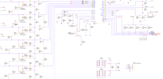
您好、Luis:
请检查随附的原理图并验证 一次。
此外、我还附上了100A 电流的日志。
e2e.ti.com/.../12V_5F00_100Amp.log
您是否没有将电池连接到 VC10 - VC9? 该部件需要 VC10 - VC9才能连接真正的电芯。
原理图似乎为1m Ω、而不是0.5m Ω。 哪一项是正确的?
日志似乎还显示了~32000的电流、到底在那里发生了什么? 您是否具有器件的.gg 文件?
基本而言、我们并联了2个1m Ω 的并联电阻器、从而形成0.5 mOhm.e2e.ti.com/.../BQ76942_5F00_Calibration_5F00_settings_5F00_4S.gg.gg-1-_2800_1_2900_.csv
请检查.gg 文件、建议是否需要进行任何更改。
原理图显示了2个2m Ω 的分流电阻器、这些电阻器并联后可以形成1m Ω。 原理图是否不正确?
状态。 我确实看到您具有 设置:配置:DA 配置[USER_AMPS_0] 设置。 这意味着电流将以 mA 为单位进行报告。 不过、这意味着只能测量高达~32A 的电流。 因为 电流测量值只能从 –32768到+32767。
因此、如果要测量高于此值的电流、则需要更改 UserA 设置。 例如、将 Settings:Configuration:DA Configuration:[USER_AMPS_1:0]设置为0x02、以便您的当前单位(userA)为10mA。
现在、我想提醒您、该器件需要连接 VC10 - VC9才能真正连接电池。
感谢您的支持。
此问题已通过 设置:配置:DA 配置[USER_AMPS_0] 。
现在、我能够读取高达100A 的电流。
K·万赫德