This thread has been locked.
If you have a related question, please click the "Ask a related question" button in the top right corner. The newly created question will be automatically linked to this question.
https://e2e.ti.com/support/power-management-group/power-management/f/power-management-forum/1208015/lm25118-design-review-request
我需要的值:
VIN = 10 V 至24 V
7安培时 VOUT = 12V
由于一直存在输出电压在未连接时约为2伏而 MOSFET 过热的问题、因此我希望有人检查我的设计、以排除任何设计问题。
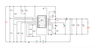
从 webench:
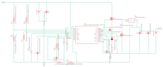
Eagle 原理图:
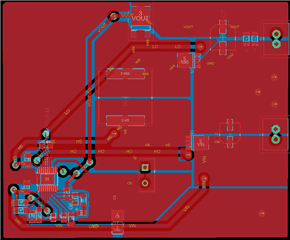
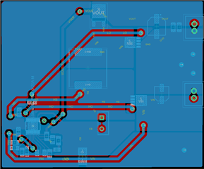
顶部:
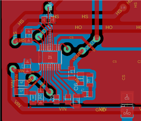
顶部缩放:
底部:
您好!
感谢您的联系。 是否已使用 Excel 快速入门计算器 https://www.ti.com/lit/zip/snvu065对该原理图进行了仔细检查 ? 对于布局,我们建议遵循数据表第35页的指导原则,即第10.2节。 您能再详细说明一下您在此电路板上看到的问题吗? 在这种情况下 MOSFET 是否过热? 如果输出电压降至2V、则器件可能处于电流限制范围内。
此致、
EM
我假设 webench 设计器使用与 Excel 文件相同的公式计算值、因此在这种情况下是这样做的。 该电路板消耗的电流过大(>4.5A)、因此我的电源 将电压限制在5伏左右以保持恒定电流。 在此电压下、MOSFET 立即开始熔化焊料。 我将电路板的几何形状设计得尽可能靠近 webench 生成的电路板、尽管第35页的10.2节看起来稍有不同。
二极管正向电压的精确度有多重要? 我必须得到一些略有不同的东西、因为它们缺货。
Josh、您好!
正向电压不是那么重要。 反向恢复电荷的影响要大得多。
如果距离很远、这很容易导致不稳定并在设计上产生电路板电感振铃
斯特凡
我使特定的板正常工作。 问题是接地不足以及 MOSFET 振铃、可能会将其烧毁。 但是、我创建了另一个小得多的版本。 我想知道是否有什么特别之处需要大线迹? webench 生成的电路板非常大。 我创建的新版本占用的空间要小得多、lm25118正变得很热。 它最初提供12伏电压、但随着时间的推移、当负载接通时可降至1.3伏、但在负载断开时从未恢复到12伏。
是否应该为 MOSFET 使用电阻器? 在 LM25118的数据表的第7.2节"功能方框图"下、我没有看到任何内容。 电阻 Rt 就是处理这一情况的方法。
对于 MOSFET、使用电阻器意味着什么? 你是说在栅极中? 这将增加功率耗散。
对于需要大线迹的电路、请查看此处的热环路:
https://e2e.ti.com/blogs_/b/powerhouse/posts/four-switch-buck-boost-layout-tip-no-1-identifying-the-critical-parts-for-layouthttps://e2e.ti.com/blogs_/b/powerhouse/posts/four-switch-buck-boost-layout-tip-no-2-optimizing-hot-loops-in-the-power-stage https://e2e.ti.com/blogs_/b/powerhouse/posts/four-switch-buck-boost-layout-tip-no-3-separating-differential-sense-lines-from-power-planes https://e2e.ti.com/blogs_/b/powerhouse/posts/four-switch-buck-boost-layout-tip-no-4-routing-gate-drive-and-return-paths
尤其是热回路(2号)需要宽布线。
此致、 布里吉特