

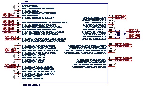
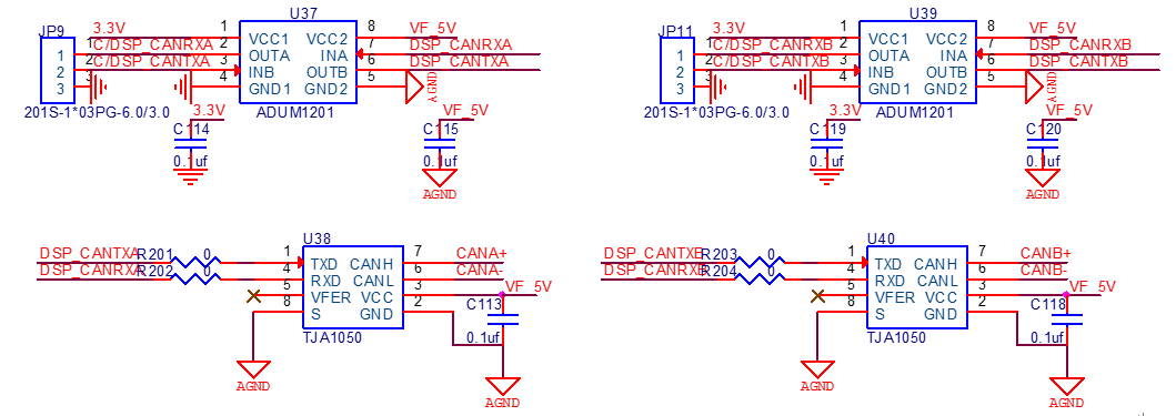
自制的板子28335 CAN接口原理如图所示,A路使用引脚GPIO18和GPIO19,B路使用引脚GPIO12和GPIO13,在端口处将CANA+和CANB+相连,CANA-和CANB-相连,并在CANA+和CANA-之间并联120欧的电阻,调试附件工程,即A路发送0X55555555和0XAAAAAAAA,B路接收,发现异常描述如下:
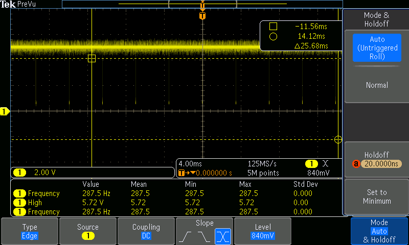
1、 该工程在开发板上测试正常,在开发板上测试TXD波形如图
2、 自制板子的串口和指示灯等功能都正常,仿真器的连接正常
3、 自制的板子和开发板的CANA和CANB接口引脚相同,但是自制的板子CAN接口异常,具体表现在A路TA无法置位
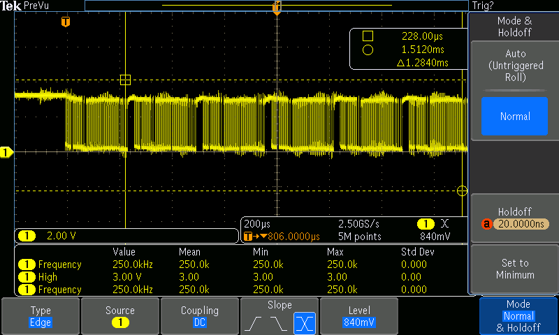
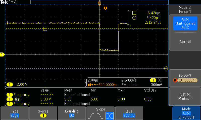
4、 直接测量A路TXD波形,约每隔3.8ms有一次宽度约2us的低电平,波形如图所示:
5、 尝试改成B发送,测量B路TXD的波形和上面波形一致,尝试将A路CAN用GPIO30和GPIO31,现象一样
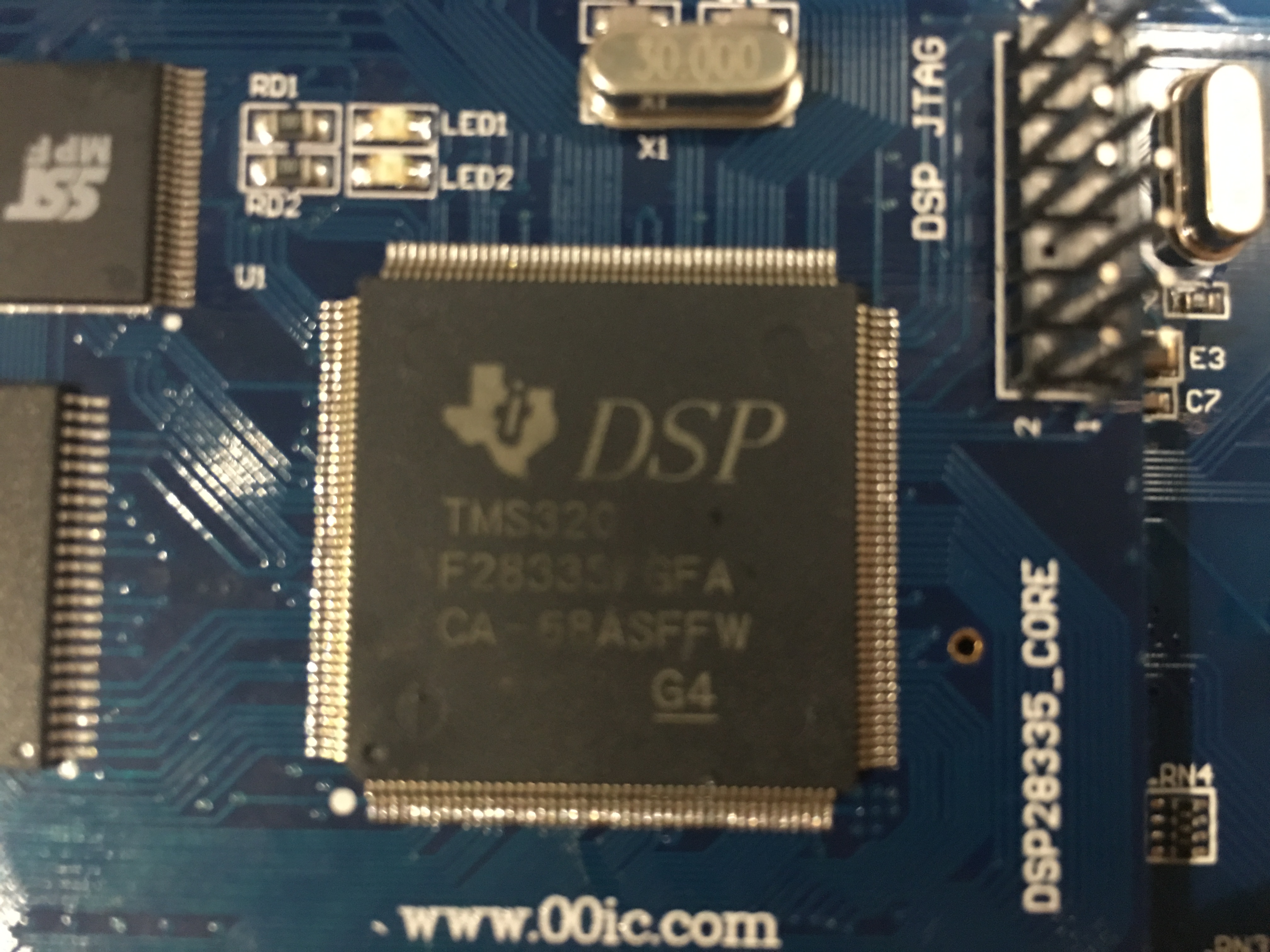
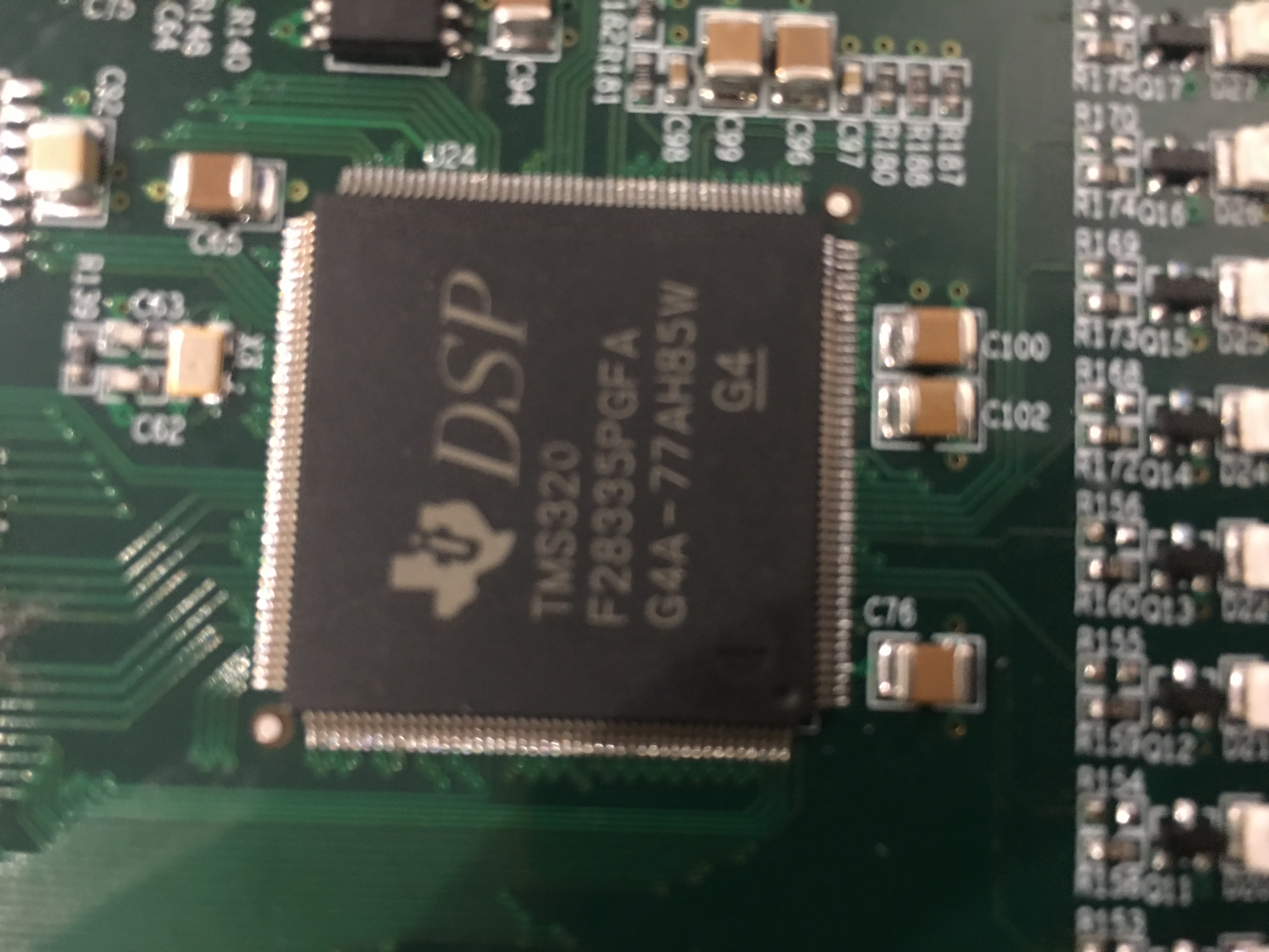
6、 比较开发板和自制板子区别,发现芯片丝印不同,开发板上的芯片批次号是CA,而自制板子芯片批次号是G4A,如图所示:
请问一下自制板子CAN不行是怎么回事?
// TI File $Revision: /main/8 $
// Checkin $Date: August 10, 2007   09:04:22 $
//###########################################################################
// Filename: Example_28xEcan_A_to_B_Xmit.c
//
// Description: eCAN-A To eCAN-B TXLOOP - Transmit loop
//
// ASSUMPTIONS:
//
//    This program requires the DSP2833x header files.
//
//    Both CAN ports of the 2833x DSP need to be connected
//    to each other (via CAN transceivers)
//
//       eCANA is on GPIO19(CANTXA)  and
//                   GPIO18 (CANRXA)
//
//       eCANB is on GPIO20  (CANTXB)  and
//                   GPIO21 (CANRXB)
//
//    As supplied, this project is configured for "boot to SARAM"
//    operation.  The 2833x Boot Mode table is shown below.
//    For information on configuring the boot mode of an eZdsp,
//    please refer to the documentation included with the eZdsp,
//
//       $Boot_Table:
//
//         GPIO87   GPIO86     GPIO85   GPIO84
//          XA15     XA14       XA13     XA12
//           PU       PU         PU       PU
//        ==========================================
//            1        1          1        1    Jump to Flash
//            1        1          1        0    SCI-A boot
//            1        1          0        1    SPI-A boot
//            1        1          0        0    I2C-A boot
//            1        0          1        1    eCAN-A boot
//            1        0          1        0    McBSP-A boot
//            1        0          0        1    Jump to XINTF x16
//            1        0          0        0    Jump to XINTF x32
//            0        1          1        1    Jump to OTP
//            0        1          1        0    Parallel GPIO I/O boot
//            0        1          0        1    Parallel XINTF boot
//            0        1          0        0    Jump to SARAM	    <- "boot to SARAM"
//            0        0          1        1    Branch to check boot mode
//            0        0          1        0    Boot to flash, bypass ADC cal
//            0        0          0        1    Boot to SARAM, bypass ADC cal
//            0        0          0        0    Boot to SCI-A, bypass ADC cal
//                                              Boot_Table_End$
//
// DESCRIPTION:
//
//    This example TRANSMITS data to another CAN module using MAILBOX5
//    This program could either loop forever or transmit "n" # of times,
//    where "n" is the TXCOUNT value.
//
//    This example can be used to check CAN-A and CAN-B. Since CAN-B is
//    initialized in DSP2833x_ECan.c, it will acknowledge all frames
//    transmitted by the node on which this code runs. Both CAN ports of
//    the 2833x DSP need to be connected to each other (via CAN transceivers)
//
//###########################################################################
// Original Author: HJ
//
// $TI Release: DSP2833x Header Files V1.10 $
// $Release Date: February 15, 2008 $
//###########################################################################

#include "DSP2833x_Device.h"     // DSP2833x Headerfile Include File
#include "DSP2833x_Examples.h"   // DSP2833x Examples Include File

#define TXCOUNT  100  // Transmission will take place (TXCOUNT) times..
#define LED1  GpioDataRegs.GPATOGGLE.bit.GPIO4
#define LED2  GpioDataRegs.GPATOGGLE.bit.GPIO5
#define LED3  GpioDataRegs.GPATOGGLE.bit.GPIO6
#define LED4  GpioDataRegs.GPATOGGLE.bit.GPIO7
// Globals for this example
long      i,j;
long 	  loopcount = 0;
volatile struct MBOX *Mailbox;
Uint32  ErrorCount;
Uint32  PassCount;
Uint32  MessageReceivedCount;

Uint32  TestMbox1 = 0;
Uint32  TestMbox2 = 0;
Uint32  TestMbox3 = 0;


void mailbox_check(int32 T1, int32 T2, int32 T3)
{
    if((T1 !=0x55555555 ) || ( T2 != 0xAAAAAAAA)|| ( T3 != 0x95555555))
    {
       ErrorCount++;
    }
    else
    {
       PassCount++;
    }
}


void main()
{

/* Create a shadow register structure for the CAN control registers. This is
 needed, since, only 32-bit access is allowed to these registers. 16-bit access
 to these registers could potentially corrupt the register contents. This is
 especially true while writing to a bit (or group of bits) among bits 16 - 31 */

   struct ECAN_REGS ECanaShadow;
	struct ECAN_REGS ECanbShadow;
// Step 1. Initialize System Control:
// PLL, WatchDog, enable Peripheral Clocks
// This example function is found in the DSP2833x_SysCtrl.c file.
   InitSysCtrl();

   EALLOW;
   GpioCtrlRegs.GPAMUX1.bit.GPIO4 = 0;
   GpioCtrlRegs.GPADIR.bit.GPIO4 = 1;
   GpioCtrlRegs.GPAMUX1.bit.GPIO5 = 0;
   GpioCtrlRegs.GPADIR.bit.GPIO5 = 1;
   GpioCtrlRegs.GPAMUX1.bit.GPIO6 = 0;
   GpioCtrlRegs.GPADIR.bit.GPIO6 = 1;
   GpioCtrlRegs.GPAMUX1.bit.GPIO7 = 0;
   GpioCtrlRegs.GPADIR.bit.GPIO7 = 1;
   EDIS;

// Step 2. Initalize GPIO:
// This example function is found in the DSP2833x_Gpio.c file and
// illustrates how to set the GPIO to it's default state.
// InitGpio();  // Skipped for this example

   // Just initalize eCAN pins for this example
   // This function is in DSP2833x_ECan.c
   InitECanGpio();

// Step 3. Clear all interrupts and initialize PIE vector table:
// Disable CPU interrupts
   DINT;

// Initialize the PIE control registers to their default state.
// The default state is all PIE interrupts disabled and flags
// are cleared.
// This function is found in the DSP2833x_PieCtrl.c file.
   InitPieCtrl();

// Disable CPU interrupts and clear all CPU interrupt flags:
   IER = 0x0000;
   IFR = 0x0000;

// Initialize the PIE vector table with pointers to the shell Interrupt
// Service Routines (ISR).
// This will populate the entire table, even if the interrupt
// is not used in this example.  This is useful for debug purposes.
// The shell ISR routines are found in DSP2833x_DefaultIsr.c.
// This function is found in DSP2833x_PieVect.c.
   InitPieVectTable();

// Interrupts that are used in this example are re-mapped to
// ISR functions found within this file.

// No interrupts used in this example.

// Step 4. Initialize all the Device Peripherals:
// This function is found in DSP2833x_InitPeripherals.c
// InitPeripherals(); // Not required for this example

   // In this case just initalize eCAN-A and eCAN-B
   // This function is in DSP2833x_ECan.c
   InitECan();
    ErrorCount = 0;
    PassCount = 0;
    // Step 5. User specific code:

/* Write to the MSGID field  */

   ECanaMboxes.MBOX10.MSGID.all = 0x95555555; // Extended Identifier

  ECanbMboxes.MBOX10.MSGID.all = 0x95555555; // Extended Identifier
/* Configure Mailbox under test as a Transmit mailbox */

   ECanaShadow.CANMD.all = ECanaRegs.CANMD.all;
   ECanaShadow.CANMD.bit.MD10 = 0;
   ECanaRegs.CANMD.all = ECanaShadow.CANMD.all;

   ECanbShadow.CANMD.all = ECanbRegs.CANMD.all;
   ECanbShadow.CANMD.bit.MD10 = 1;
   ECanbRegs.CANMD.all = ECanbShadow.CANMD.all;

/* Enable Mailbox under test */

   ECanaShadow.CANME.all = ECanaRegs.CANME.all;
   ECanaShadow.CANME.bit.ME10 = 1;
   ECanaRegs.CANME.all = ECanaShadow.CANME.all;

   ECanbShadow.CANME.all = ECanbRegs.CANME.all;
   ECanbShadow.CANME.bit.ME10 = 1;
   ECanbRegs.CANME.all = ECanbShadow.CANME.all;

/* Write to DLC field in Master Control reg */

   ECanaMboxes.MBOX10.MSGCTRL.bit.DLC = 8;

/* Write to the mailbox RAM field */

   ECanaMboxes.MBOX10.MDL.all = 0x55555555;
   ECanaMboxes.MBOX10.MDH.all = 0xAAAAAAAA;

   ECanbMboxes.MBOX10.MSGCTRL.bit.DLC = 8;

/* Write to the mailbox RAM field */

   ECanbMboxes.MBOX10.MDL.all = 0x55555555;
   ECanbMboxes.MBOX10.MDH.all = 0xAAAAAAAA;

/* Begin transmitting */


   for(i=0; i < TXCOUNT; i++)
   {

       ECanaShadow.CANTRS.all = 0;
       ECanaShadow.CANTRS.bit.TRS10 = 1;             // Set TRS for mailbox under test
       ECanaRegs.CANTRS.all = ECanaShadow.CANTRS.all;

       do
    	{
      	ECanaShadow.CANTA.all = ECanaRegs.CANTA.all;
    	} while(ECanaShadow.CANTA.bit.TA10 == 0 );   // Wait for TA5 bit to be set..//如果线没有连接,如果线连接错误


       ECanaShadow.CANTA.all = 0;
       ECanaShadow.CANTA.bit.TA10 = 1;     	         // Clear TA5
       ECanaRegs.CANTA.all = ECanaShadow.CANTA.all;

       Mailbox = &ECanbMboxes.MBOX0 + 25;  //CANB读数据
       TestMbox1 = Mailbox->MDL.all; // = 0x (n is the MBX number)
       TestMbox2 = Mailbox->MDH.all; // = 0x (a constant)
       TestMbox3 = Mailbox->MSGID.all;// = 0x (n is the MBX number)
       mailbox_check(TestMbox1,TestMbox2,TestMbox3); // Checks the received data


       loopcount ++;
    }
      if(ErrorCount == 0)
		  {
			asm("      ESTOP0"); // OK,数据校验正确
		  }
		  else
		  {
			asm("      ESTOP0"); // ERROR,
		  }


     //asm(" ESTOP0");  // Stop here
}
