
您好,
控制板采用如下的复位电路,当我按下复位按钮后,我可以通过示波器观察到XRS引脚的电平恢复了,而PWM驱动被拉低了,无法恢复。从CCS变量观察窗口可以看见PDPINTA的值由1变为0,可是硬件上并没有焊有关PDPINT的电路,程序中也没有使能这个中断,这是怎么一回事呢?
希望得到您的解答。
谢谢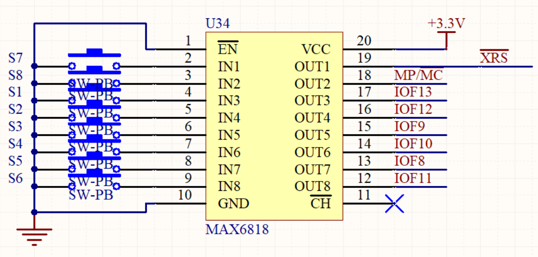


This thread has been locked.
If you have a related question, please click the "Ask a related question" button in the top right corner. The newly created question will be automatically linked to this question.
您好,
控制板采用如下的复位电路,当我按下复位按钮后,我可以通过示波器观察到XRS引脚的电平恢复了,而PWM驱动被拉低了,无法恢复。从CCS变量观察窗口可以看见PDPINTA的值由1变为0,可是硬件上并没有焊有关PDPINT的电路,程序中也没有使能这个中断,这是怎么一回事呢?
希望得到您的解答。
谢谢
如果我想采用软件中断的方式,将EXTCONA寄存器INDCOE位设为1,将三路比较单元分开控制。当采样检测电流,当大于阈值时,我需要切断6路PWM信号中的4路。在中断程序中将EvaRegs.COMCONA.bit.FCMPxOE设为0(高阻态),但是当我实验时发现,PWM信号并不能关断,请问这是怎么回事呢?
十分感谢您的耐心解答,程序我在后面附上。
// �ز���ֵ���ƿ�������
// This program is used for buck-boost inverter
// Date: Sep 8th , 2019 Version: 1.2
// Author: ZhangYuyao
// Description��
// �ɼ�ֱ�����е�����ͨ���ӳٵ��������ķ������˳�����Ƶ�ɷݡ��ڷ�����ͨ���ı��ز���ֵ��С��ɵ��ƣ�����ʵ���У���ı���Ʋ��ķ�ֵ��
#include "DSP281x_Device.h"
#include "DSP281x_Examples.h"
#include "IQmathLib.h"
#include <math.h>
#define Ts 0.00005
#define N 400 // 50*400=20000Hz �ز���Ϊ400
/*#pragma CODE_SECTION(T1_Compare_isr, "ramfuncs"); // ���жϺ���T1PINT_isrд��RAM�У���Ϊad_isr���������ã�����ʡ��ÿ�ζ���flash��д��RAM
// ������Initflash()�ij�ʼ���ͱ�д����
extern Uint16 RamfuncsLoadStart; // ��Ϊ����memcpy�����ı���������MemCopy�����еı����������ȫ�ֱ�������
extern Uint16 RamfuncsLoadEnd;
extern Uint16 RamfuncsRunStart;*/
// Variable defs
int32 idc_s; // idc_s---ֱ������е�������
int32 idc;
int32 idc_Q = 0;
int32 idc_Q1 = 0; // ����ʱ�ź�
int32 idc_Q2 = 0; // ��ʱT/4�ź�
int32 idc_avg1 = 0; // the avg value after T/4 delay
int32 idc_avg1_Q1 = 0; // ����ʱ�ź�
int32 idc_avg1_Q2 = 0; // ��ʱT/8�ź�
int32 idc_avg2 = 0; // the avg value after all delay
int32 buffer[400];
float32 coefficient_k; // ��ֵ����ϵ��
int16 i = 0;
int16 j = 0;
int16 k = 301;
int16 jj = 0;
int16 kk = 351;
int32 g1,g2,g3,P,G;
float32 Modu_Index=0.4; // Modulation index, ���Ʊ�
// Sine table
float32 sina[400]=
{
0,0.0157,0.0314,0.0471,0.0628,0.0785,0.0941,0.1097,0.1253,0.1409,0.1564,0.1719,0.1874,0.2028,0.2181,0.2334,
0.2487,0.2639,0.2790,0.2940,0.3090,0.3239,0.3387,0.3535,0.3681,0.3827,0.3971,0.4115,0.4258,0.4399,0.4540,
0.4679,0.4818,0.4955,0.5090,0.5225,0.5358,0.5490,0.5621,0.5750,0.5878,0.6004,0.6129,0.6252,0.6374,0.6494,
0.6613,0.6730,0.6845,0.6959,0.7071,0.7181,0.7290,0.7396,0.7501,0.7604,0.7705,0.7804,0.7902,0.7997,0.8090,
0.8181,0.8271,0.8358,0.8443,0.8526,0.8607,0.8686,0.8763,0.8838,0.8910,0.8980,0.9048,0.9114,0.9178,0.9239,
0.9298,0.9354,0.9409,0.9461,0.9511,0.9558,0.9603,0.9646,0.9686,0.9724,0.9759,0.9792,0.9823,0.9851,0.9877,
0.9900,0.9921,0.9940,0.9956,0.9969,0.9980,0.9989,0.9995,0.9999,1.0000,0.9999,0.9995,0.9989,0.9980,0.9969,
0.9956,0.9940,0.9921,0.9900,0.9877,0.9851,0.9823,0.9792,0.9759,0.9724,0.9686,0.9646,0.9603,0.9558,0.9511,
0.9461,0.9409,0.9354,0.9298,0.9239,0.9178,0.9114,0.9048,0.8980,0.8910,0.8838,0.8763,0.8686,0.8607,0.8526,
0.8443,0.8358,0.8271,0.8181,0.8090,0.7997,0.7902,0.7804,0.7705,0.7604,0.7501,0.7396,0.7290,0.7181,0.7071,
0.6959,0.6845,0.6730,0.6613,0.6494,0.6374,0.6252,0.6129,0.6004,0.5878,0.5750,0.5621,0.5490,0.5358,0.5225,
0.5090,0.4955,0.4818,0.4679,0.4540,0.4399,0.4258,0.4115,0.3971,0.3827,0.3681,0.3535,0.3387,0.3239,0.3090,
0.2940,0.2790,0.2639,0.2487,0.2334,0.2181,0.2028,0.1874,0.1719,0.1564,0.1409,0.1253,0.1097,0.0941,0.0785,
0.0628,0.0471,0.0314,0.0157,0,-0.0157,-0.0314,-0.0471,-0.0628,-0.0785,-0.0941,-0.1097,-0.1253,-0.1409,
-0.1564,-0.1719,-0.1874,-0.2028,-0.2181,-0.2334,-0.2487,-0.2639,-0.2790,-0.2940,-0.3090,-0.3239,-0.3387,
-0.3535,-0.3681,-0.3827,-0.3971,-0.4115,-0.4258,-0.4399,-0.4540,-0.4679,-0.4818,-0.4955,-0.5090,-0.5225,
-0.5358,-0.5490,-0.5621,-0.5750,-0.5878,-0.6004,-0.6129,-0.6252,-0.6374,-0.6494,-0.6613,-0.6730,-0.6845,
-0.6959,-0.7071,-0.7181,-0.7290,-0.7396,-0.7501,-0.7604,-0.7705,-0.7804,-0.7902,-0.7997,-0.8090,-0.8181,
-0.8271,-0.8358,-0.8443,-0.8526,-0.8607,-0.8686,-0.8763,-0.8838,-0.8910,-0.8980,-0.9048,-0.9114,-0.9178,
-0.9239,-0.9298,-0.9354,-0.9409,-0.9461,-0.9511,-0.9558,-0.9603,-0.9646,-0.9686,-0.9724,-0.9759,-0.9792,
-0.9823,-0.9851,-0.9877,-0.9900,-0.9921,-0.9940,-0.9956,-0.9969,-0.9980,-0.9989,-0.9995,-0.9999,-1.0000,
-0.9999,-0.9995,-0.9989,-0.9980,-0.9969,-0.9956,-0.9940,-0.9921,-0.9900,-0.9877,-0.9851,-0.9823,-0.9792,
-0.9759,-0.9724,-0.9686,-0.9646,-0.9603,-0.9558,-0.9511,-0.9461,-0.9409,-0.9354,-0.9298,-0.9239,-0.9178,
-0.9114,-0.9048,-0.8980,-0.8910,-0.8838,-0.8763,-0.8686,-0.8607,-0.8526,-0.8443,-0.8358,-0.8271,-0.8181,
-0.8090,-0.7997,-0.7902,-0.7804,-0.7705,-0.7604,-0.7501,-0.7396,-0.7290,-0.7181,-0.7071,-0.6959,-0.6845,
-0.6730,-0.6613,-0.6494,-0.6374,-0.6252,-0.6129,-0.6004,-0.5878,-0.5750,-0.5621,-0.5490,-0.5358,-0.5225,
-0.5090,-0.4955,-0.4818,-0.4679,-0.4540,-0.4399,-0.4258,-0.4115,-0.3971,-0.3827,-0.3681,-0.3535,-0.3387,
-0.3239,-0.3090,-0.2940,-0.2790,-0.2639,-0.2487,-0.2334,-0.2181,-0.2028,-0.1874,-0.1719,-0.1564,-0.1409,
-0.1253,-0.1097,-0.0941,-0.0785,-0.0628,-0.0471,-0.0314,-0.0157
};
// ��������
interrupt void T1_Compare_isr(void);
void AD_Sampling(void);
void Carrier_Modulation(void);
void SPWM(void);
void PROTECT_PDPINTA_ISR(void);
void main(void)
{
// Step 1. Initialize System Control:
// PLL, WatchDog, enable Peripheral Clocks
// This example function is found in the DSP281x_SysCtrl.c file.
InitSysCtrl();
//��memcpy֮��ִ��Initflash()��������д��Ĺ��ܺ���
//MemCopy(&RamfuncsLoadStart, &RamfuncsLoadEnd, &RamfuncsRunStart);
//InitFlash();
// Step 2. Initalize GPIO:
// This example function is found in the DSP281x_Gpio.c file and
// illustrates how to set the GPIO to it's default state.
InitGpio();
// Step 3. Clear all interrupts and initialize PIE vector table:
// Disable CPU interrupts
DINT;
// Initialize PIE control registers to their default state.
// The default state is all PIE interrupts disabled and flags
// are cleared.
// This function is found in the DSP281x_PieCtrl.c file.
InitPieCtrl();
// Disable CPU interrupts and clear all CPU interrupt flags:
IER=0x0000;
IFR=0x0000;
// Initialize the PIE vector table with pointers to the shell Interrupt
// Service Routines (ISR).
// This will populate the entire table, even if the interrupt
// is not used in this example. This is useful for debug purposes.
// The shell ISR routines are found in DSP281x_DefaultIsr.c.
// This function is found in DSP281x_PieVect.c.
InitPieVectTable();
// Interrupts that are used in this example are re-mapped to
// ISR functions found within this file.
EALLOW; // This is needed to write to EALLOW protected registers
PieVectTable.T1PINT=&T1_Compare_isr;
EDIS; // This is needed to disable write to EALLOW protected registers
// Step 4. Initialize all the Device Peripherals:
// This function is found in DSP281x_InitPeripherals.c
// InitPeripherals(); // Not required for this example
InitEv();
InitAdc();
// Step 5. User specific code, enable interrupts:
PieCtrlRegs.PIEIER2.all=M_INT4; // PIE interrupt enable,T1��ʱ���ж�λ��INT2.4
IER|=M_INT2;
// Enable global Interrupts and higher priority real-time debug events:
EINT; // Enable Global interrupt INTM
ERTM; // Enable Global realtime interrupt DBGM
EvaRegs.T1CON.bit.TENABLE = 1; // Timer1 number counter enable
// Step 6. Just sit and loop forever:
for(;;);
}
// ADC������
void AD_Sampling(void)
{
idc_s=(AdcRegs.ADCRESULT0>>4);//���������ӽ�20A,��������Ϊ51ŷʱ��A6ͨ��
idc=(idc_s-2092+15);
idc_Q=_IQmpy(_IQ(idc),_IQ(0.01436472));
}
void Carrier_Modulation(void)
{
// delay time T/4
if (j<N)
{
buffer[j]=idc_Q;
j++;
}
else
{
j=0;
}
if (k<N)
{
idc_Q1=idc_Q;
idc_Q2=buffer[k];
k++;
}
else
{
k=0;
}
idc_avg1=_IQmpy(idc_Q1+idc_Q2,_IQ(0.5));
// delay time T/8
if (jj<N)
{
buffer[jj]=idc_avg1;
jj++;
}
else
{
jj=0;
}
if (kk<N)
{
idc_avg1_Q1=idc_avg1;
idc_avg1_Q2=buffer[kk];
kk++;
}
else
{
kk=0;
}
idc_avg2=_IQmpy(idc_avg1_Q1+idc_avg1_Q2,_IQ(0.5));
coefficient_k=_IQdiv(idc_avg2,idc_Q); // ������ѡ�����ز����Է�ֵ����ϵ��k1��k1=idc˲ʱֵ/idcƽ��ֵ��ʵ����ѡ���ɵ��Ʋ����Է�ֵ����ϵ��k��k=1/k1��
if (coefficient_k<=_IQ(0.5))
{
coefficient_k=_IQ(0.5);
}
if (coefficient_k>=_IQ(2.5))
{
coefficient_k=_IQ(2.5);
}
}
void SPWM(void)
{
P=_IQmpy(_IQ(sina[i]),_IQ(Modu_Index));
G=_IQmpy(P,coefficient_k);
//G=_IQmpy(_IQ(sina[i]),_IQ(Modu_Index));//�������
if (G>=0)
{
g1=(int)((long)3750*G>>18); // S5,S6�����ܸ�Ƶ, ��ʵ��ʱ��Ҫ�������ߣ��ϵ�ʱע����������������DSP G2
//g1=3751;
//g2=(int)((long)3750*G>>18); // S2,S3�����ܸ�Ƶ, ��DSP G3
g2 = 3751;//��Ƶ
g3=0; // S1,S4�����ܵ͵�ƽ, ��DSP G5
}
if (G<0)
{
g1=(int)((long)3750*(-G)>>18); // S5,S6�����ܸ�Ƶ, �����ܵ��Ʋ�ȡABS
//g1=0;
g2=0; // S2,S3�����ܵ͵�ƽ
g3 = 3751;//��Ƶ
//g3=(int)((long)3750*(-G)>>18); // S1,S4�����ܸ�Ƶ
}
i++;
if (i>=N)
{
i=0;
}
if (g1<=0)
g1=0;
if (g1>=3750)
g1=3750;
if (g2<=0)
g2=0;
if (g2>=3750)
g2=3750;
if (g3<=0)
g3=0;
if (g3>=3750)
g3=3750;
EvaRegs.CMPR1=g1;
EvaRegs.CMPR2=g2;
EvaRegs.CMPR3=g3;
}
void PROTECT_PDPINTA_ISR(void) // EV-A, INT1.1
{
// Insert ISR Code here, ��GPIO���Ž������ߺ����ͣ��������ʱ��S1/4�㵼ͨ��S2/3/5�ض�
if (idc_Q>=_IQ(5.5))
{
EvaRegs.COMCONA.bit.FCMP1OE = 0;
EvaRegs.COMCONA.bit.FCMP2OE = 1;
EvaRegs.COMCONA.bit.FCMP3OE = 0;
}
if (idc_Q<_IQ(5.5))
{
}
}
interrupt void T1_Compare_isr(void)
{
AD_Sampling();
Carrier_Modulation();
SPWM();
PROTECT_PDPINTA_ISR();
//DA_Viewer();
EvaRegs.EVAIFRA.bit.T1PINT=1; // ���T1�����ж��еı�־λ
PieCtrlRegs.PIEACK.bit.ACK2=1; // ��Ӧͬ���ж�
EINT; // ��ȫ���ж�
}
// TI File $Revision: /main/2 $
// Checkin $Date: April 29, 2005   11:10:23 $
//###########################################################################
//
// FILE:	DSP281x_Ev.c
//
// TITLE:	DSP281x Event Manager Initialization & Support Functions.
//
//###########################################################################
// $TI Release: DSP281x C/C++ Header Files V1.20 $
// $Release Date: July 27, 2009 $
//###########################################################################

#include "DSP281x_Device.h"     // DSP281x Headerfile Include File
#include "DSP281x_Examples.h"   // DSP281x Examples Include File

//---------------------------------------------------------------------------
// InitEv:
//---------------------------------------------------------------------------
// This function initializes to a known state.
//
void InitEv(void)
{

// EVA Configure T1PWM, T2PWM, PWM1-PWM6

	  // Initalize the timers
	  // Initalize EVA Timer1
	  EvaRegs.T1PR = 3750;          // Timer1 period, the frequency of carrier is 20kHz
	  EvaRegs.T1CMPR = 0x0000;      // Timer1 compare
	  EvaRegs.T1CNT = 0x0000;       // Timer1 counter

	  EvaRegs.T1CON.bit.TMODE=1;    // TMODE = continuous up/down
	  EvaRegs.T1CON.bit.TPS=0;      // T1CLK = HSPCLK/1 = 150MHz
	  EvaRegs.T1CON.bit.TENABLE=0;  // Timer disable
	  EvaRegs.T1CON.bit.TCLKS10=0;  // Select the internal clock
	  EvaRegs.T1CON.bit.TECMPR=1;   // Timer compare enable

	  // Setup T1PWM and T2PWM
	  // Drive T1/T2 PWM by compare logic
//	  EvaRegs.GPTCONA.bit.TCMPOE = 1;
	  // Polarity of GP Timer 1 Compare = Active low
//	  EvaRegs.GPTCONA.bit.T1PIN = 1;
	  // Polarity of GP Timer 2 Compare = Active high
//	  EvaRegs.GPTCONA.bit.T2PIN = 2;
	  EvaRegs.GPTCONA.bit.T1TOADC=2;   // ��������ADC

	  // Enable compare for PWM1-PWM6
	  EvaRegs.CMPR1 = 0x0000;
	  EvaRegs.CMPR2 = 0x0000;
	  EvaRegs.CMPR3 = 0x0000;

	  // Compare action control.  Action that takes place
	  // on a cmpare event
	  // output pin 1 CMPR1 - active high
	  // output pin 2 CMPR1 - active low
	  // output pin 3 CMPR2 - active high
	  // output pin 4 CMPR2 - active low
	  // output pin 5 CMPR3 - active high
	  // output pin 6 CMPR3 - active low
	  //EvaRegs.ACTRA.all = 0x0666;

	  EvaRegs.ACTRA.all = 0x0999;

	  //EvaRegs.DBTCONA.all = 0x0000;    // Disable deadband

/*	  Overlap_time 1us   */
	  EvaRegs.DBTCONA.bit.DBT = 6;
	  EvaRegs.DBTCONA.bit.EDBT1 = 1;
	  EvaRegs.DBTCONA.bit.EDBT2 = 1;
	  EvaRegs.DBTCONA.bit.EDBT3 = 1;
	  EvaRegs.DBTCONA.bit.DBTPS = 5;

	  EvaRegs.COMCONA.bit.CENABLE=1;   // ʹ�ܱȽϵ�Ԫ�ıȽϲ���
	  //EvaRegs.COMCONA.bit.FCOMPOE=1;   // ȫ�Ƚ����ʹ��
	  EvaRegs.COMCONA.bit.CLD=2;

	  EvaRegs.EVAIMRA.bit.T1PINT=1;  // Timer1 period interrupt enable
	  EvaRegs.EVAIFRA.bit.T1PINT=1;  // ���T1�����ж��еı�־λ

/*	  Protect   */
	  EvaRegs.COMCONA.bit.PDPINTASTATUS;
	  //EvaRegs.EVAIMRA.bit.PDPINTA=1;  // PDPINTA interrupt enable

	  EvaRegs.EXTCONA.bit.INDCOE =1;  // ȫ�Ƚ������Ϊ�����ֵ�������
	  EvaRegs.COMCONA.bit.FCMP1OE = 1;
	  EvaRegs.COMCONA.bit.FCMP2OE = 1;
	  EvaRegs.COMCONA.bit.FCMP3OE = 1;
}

//===========================================================================
// No more.
//===========================================================================
// TI File $Revision: /main/2 $
// Checkin $Date: April 29, 2005 11:11:45 $
//###########################################################################
//
// FILE: DSP281x_Adc.c
//
// TITLE: DSP281x ADC Initialization & Support Functions.
//
//###########################################################################
// $TI Release: DSP281x C/C++ Header Files V1.20 $
// $Release Date: July 27, 2009 $
//###########################################################################
#include "DSP281x_Device.h" // DSP281x Headerfile Include File
#include "DSP281x_Examples.h" // DSP281x Examples Include File
#define ADC_usDELAY 8000L
#define ADC_usDELAY2 20L
//---------------------------------------------------------------------------
// InitAdc:
//---------------------------------------------------------------------------
// This function initializes ADC to a known state.
//
void InitAdc(void)
{
extern void DSP28x_usDelay(Uint32 Count);
// To powerup the ADC the ADCENCLK bit should be set first to enable
// clocks, followed by powering up the bandgap and reference circuitry.
// After a 5ms delay the rest of the ADC can be powered up. After ADC
// powerup, another 20us delay is required before performing the first
// ADC conversion. Please note that for the delay function below to
// operate correctly the CPU_CLOCK_SPEED define statement in the
// DSP28_Examples.h file must contain the correct CPU clock period in
// nanoseconds. For example:
AdcRegs.ADCTRL1.bit.RESET = 1; // reset the ADC
asm(" RPT #0 || NOP"); // one cycle
AdcRegs.ADCTRL1.bit.RESET = 0;
AdcRegs.ADCTRL3.bit.ADCBGRFDN = 0x3; // Power up bandgap/reference circuitry
DELAY_US(ADC_usDELAY); // Delay before powering up rest of ADC
AdcRegs.ADCTRL3.bit.ADCPWDN = 1; // Power up rest of ADC
DELAY_US(ADC_usDELAY2); // Delay after powering up ADC
/*AdcRegs.ADCTRL1.bit.RESET = 1; // reset the ADC
asm(" RPT #0 || NOP"); // one cycle
AdcRegs.ADCTRL1.bit.RESET = 0;*/
AdcRegs.ADCTRL1.bit.SUSMOD = 3; // ������ͣʱ�����з��������������ֵ�·������ֹͣ
AdcRegs.ADCTRL1.bit.ACQ_PS = 2; // S/H width in ADC module periods = (ACQ_PS+1)/ADCLK = 1.2 us
AdcRegs.ADCTRL1.bit.CPS = 1; // �ں�ʱ���ٽ���һ�ζ���Ƶ
AdcRegs.ADCTRL3.bit.ADCCLKPS = 15; // ADC module clock = HSPCLK/(2*ADCCLKPS)*(CPS+1)=2.5 MHz
AdcRegs.ADCTRL1.bit.CONT_RUN = 1; // 0,���/ֹͣģʽ 1,����ģʽ
AdcRegs.ADCTRL1.bit.SEQ_CASC = 1; // 0 Dual Sequencer Mode, 1 Cascaded Mode
AdcRegs.ADCTRL3.bit.SMODE_SEL = 0; // 0 Sequential Sampling Mode, 1 Simultaneous Sampling Mode
AdcRegs.ADCMAXCONV.bit.MAX_CONV1 = 0; // ������·
AdcRegs.ADCCHSELSEQ1.bit.CONV00 = 0x6; // ADCINA6
AdcRegs.ADCST.bit.INT_SEQ1_CLR = 1; // ���SEQ1���жϱ�־λ
AdcRegs.ADCST.bit.INT_SEQ2_CLR = 1; // ���SEQ2���жϱ�־λ
AdcRegs.ADCTRL2.bit.EVA_SOC_SEQ1 = 1; // Allows SEQ1/SEQ to be started by Event Manager A trigger
AdcRegs.ADCTRL2.bit.EVB_SOC_SEQ = 0; // EVB SOC enable for cascaded sequencer (Note: This bit is active only in cascaded mode.) 0, No action.
AdcRegs.ADCTRL2.bit.EVB_SOC_SEQ2 = 0; // Event Manager B SOC mask bit for SEQ2. 0, SEQ2 cannot be started by EVB trigger.
AdcRegs.ADCTRL2.bit.EXT_SOC_SEQ1 = 0; // External signal start-of-conversion bit for SEQ1. 0, No action.
AdcRegs.ADCTRL2.bit.INT_ENA_SEQ1 = 0; // SEQ1 interrupt enable. This bit enables the interrupt request to CPU by INT SEQ1.
AdcRegs.ADCTRL2.bit.INT_ENA_SEQ2 = 0; // SEQ2 interrupt disable. This bit enables or disables an interrupt request to the CPU by INT SEQ2.
AdcRegs.ADCTRL2.bit.INT_MOD_SEQ1 = 0; // SEQ1 interrupt mode. 0, INT SEQ1 is set at the end of every SEQ1 sequence.
AdcRegs.ADCTRL2.bit.INT_MOD_SEQ2 = 0; // SEQ2 interrupt mode. 0, INT SEQ2 is set at the end of every SEQ2 sequence.
AdcRegs.ADCTRL2.bit.RST_SEQ1 = 0; // Reset sequencer1
AdcRegs.ADCTRL2.bit.RST_SEQ2 = 0; // Reset sequencer2 0, No action.
AdcRegs.ADCTRL2.bit.SOC_SEQ1 = 1; // Start of conversion (SOC) trigger for Sequencer 1 (SEQ1).
AdcRegs.ADCTRL2.bit.SOC_SEQ2 = 0; // Start of conversion trigger for sequencer 2 (SEQ2). (Only applicable in dual-sequencer mode; ignored in cascaded mode.) 0 Clears a Pending SOC trigger
}
//===========================================================================
// No more.
//===========================================================================


