
尊敬的工程师:
您好,关于DMA的触发源,是不是DMA的触发源只是监测外设的中断的标志位(无论中断是否使能)。我有个疑问,DMA触发在内部监测的是不是中断的标志位,是不是和中断是同一个标志位?谢谢。
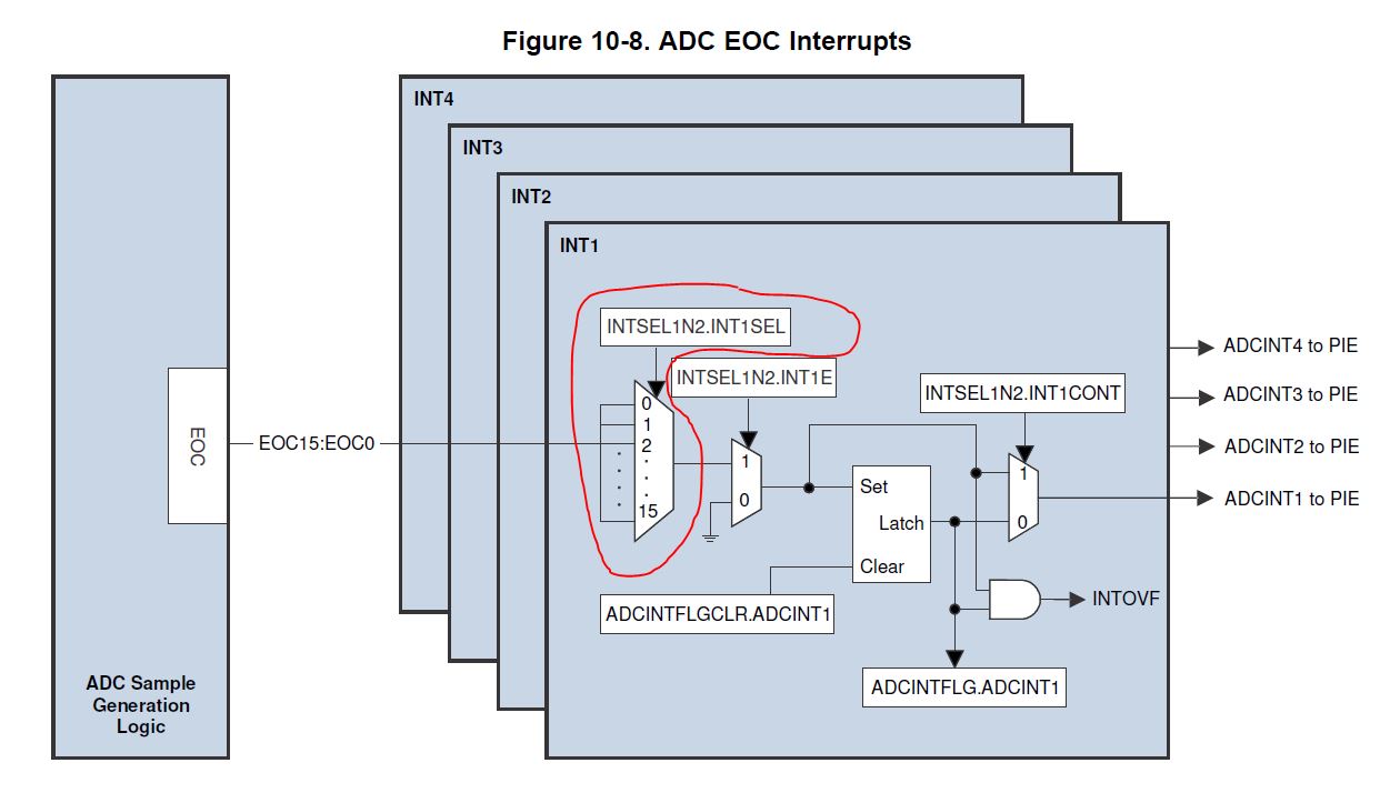
如果对于使用AD的INT1触发DMA传输,如下图所示,是不是在AD的寄存器中只需要设置图中画红圈的那部分寄存器就可以了,图中其它部分的寄存器不需要设置了,是这样子吗,非常感谢!
祝您好心情!

This thread has been locked.
If you have a related question, please click the "Ask a related question" button in the top right corner. The newly created question will be automatically linked to this question.
尊敬的工程师:
您好,关于DMA的触发源,是不是DMA的触发源只是监测外设的中断的标志位(无论中断是否使能)。我有个疑问,DMA触发在内部监测的是不是中断的标志位,是不是和中断是同一个标志位?谢谢。
如果对于使用AD的INT1触发DMA传输,如下图所示,是不是在AD的寄存器中只需要设置图中画红圈的那部分寄存器就可以了,图中其它部分的寄存器不需要设置了,是这样子吗,非常感谢!
祝您好心情!
是的,您的理解是正确的。
DMA的作用是在不影响CPU工作的前提下,搬移数据,所以当某触发源,如ADCINT1信号发生的时候,DMA机制就自动去搬移这些数据。具体使用的话,您可以参考附件内的代码
//###########################################################################
//
// FILE:   adc_soc_continuous_dma_cpu01.c
//
// TITLE:  ADC continuous conversions read by DMA for F2837xD.
//
//! \addtogroup cpu01_example_list
//! <h1> ADC Continuous Conversions Read by DMA (adc_soc_continuous_dma)</h1>
//!
//! This example sets up two ADC channels to convert simultaneously. The
//! results will be transferred by the DMA into a buffer in RAM.
//!
//! After the program runs, the memory will contain:
//!
//! - \b adcData0 \b: a digital representation of the voltage on pin A3\n
//! - \b adcData1 \b: a digital representation of the voltage on pin B3\n
//!
//
//###########################################################################
// $TI Release: F2837xD Support Library v3.03.00.00 $
// $Release Date: Thu Dec  7 18:51:32 CST 2017 $
// $Copyright:
// Copyright (C) 2013-2017 Texas Instruments Incorporated - http://www.ti.com/
//
// Redistribution and use in source and binary forms, with or without
// modification, are permitted provided that the following conditions
// are met:
//
//   Redistributions of source code must retain the above copyright
//   notice, this list of conditions and the following disclaimer.
//
//   Redistributions in binary form must reproduce the above copyright
//   notice, this list of conditions and the following disclaimer in the
//   documentation and/or other materials provided with the
//   distribution.
//
//   Neither the name of Texas Instruments Incorporated nor the names of
//   its contributors may be used to endorse or promote products derived
//   from this software without specific prior written permission.
//
// THIS SOFTWARE IS PROVIDED BY THE COPYRIGHT HOLDERS AND CONTRIBUTORS
// "AS IS" AND ANY EXPRESS OR IMPLIED WARRANTIES, INCLUDING, BUT NOT
// LIMITED TO, THE IMPLIED WARRANTIES OF MERCHANTABILITY AND FITNESS FOR
// A PARTICULAR PURPOSE ARE DISCLAIMED. IN NO EVENT SHALL THE COPYRIGHT
// OWNER OR CONTRIBUTORS BE LIABLE FOR ANY DIRECT, INDIRECT, INCIDENTAL,
// SPECIAL, EXEMPLARY, OR CONSEQUENTIAL DAMAGES (INCLUDING, BUT NOT
// LIMITED TO, PROCUREMENT OF SUBSTITUTE GOODS OR SERVICES; LOSS OF USE,
// DATA, OR PROFITS; OR BUSINESS INTERRUPTION) HOWEVER CAUSED AND ON ANY
// THEORY OF LIABILITY, WHETHER IN CONTRACT, STRICT LIABILITY, OR TORT
// (INCLUDING NEGLIGENCE OR OTHERWISE) ARISING IN ANY WAY OUT OF THE USE
// OF THIS SOFTWARE, EVEN IF ADVISED OF THE POSSIBILITY OF SUCH DAMAGE.
// $
//###########################################################################

//
// Included Files
//
#include "F28x_Project.h"

//
// Function Prototypes
//
__interrupt void adca1_isr(void);
__interrupt void dmach1_isr(void);

void ConfigureEPWM(void);
void ConfigureADC(void);
void SetupADCContinuous(volatile struct ADC_REGS * adcRegs, Uint16 channel);
void DMAInit(void);

//
// Defines
//
#define RESULTS_BUFFER_SIZE 1024    // Buffer for storing conversion results
                                    // (size must be multiple of 16)

//
// Globals
//
#pragma DATA_SECTION(adcData0, "ramgs0");
#pragma DATA_SECTION(adcData1, "ramgs0");
Uint16 adcData0[RESULTS_BUFFER_SIZE];
Uint16 adcData1[RESULTS_BUFFER_SIZE];
volatile Uint16 done;

void main(void)
{
    Uint16 resultsIndex;

//
// Step 1. Initialize System Control:
// PLL, WatchDog, enable Peripheral Clocks
// This example function is found in the F2837xD_SysCtrl.c file.
//
    InitSysCtrl();

//
// Step 2. Initialize GPIO:
// This example function is found in the F2837xD_Gpio.c file and
// illustrates how to set the GPIO to it's default state.
//
    InitGpio();

//
// Step 3. Clear all interrupts and initialize PIE vector table:
// Disable CPU interrupts
//
    DINT;

//
// Initialize the PIE control registers to their default state.
// The default state is all PIE interrupts disabled and flags
// are cleared.
// This function is found in the F2837xD_PieCtrl.c file.
//
    InitPieCtrl();

//
// Disable CPU interrupts and clear all CPU interrupt flags:
//
    IER = 0x0000;
    IFR = 0x0000;

//
// Initialize the PIE vector table with pointers to the shell Interrupt
// Service Routines (ISR).
// This will populate the entire table, even if the interrupt
// is not used in this example.  This is useful for debug purposes.
// The shell ISR routines are found in F2837xD_DefaultIsr.c.
// This function is found in F2837xD_PieVect.c.
//
    InitPieVectTable();

//
// Set up ISRs used by this example
//
// ISR for ADCA INT1 - occurs after first conversion
// ISR for DMA ch1 - occurs when DMA transfer is complete
//
    EALLOW;
    PieVectTable.ADCA1_INT = &adca1_isr;
    PieVectTable.DMA_CH1_INT = &dmach1_isr;
    EDIS;

//
// Enable specific CPU interrupts: INT1 for ADCs and INT7 for DMA
//
    IER |= M_INT1;
    IER |= M_INT7;

//
// Enable specific PIE interrupts
//
// ADCA INT1 - Group 1, interrupt 1
// DMA interrupt - Group 7, interrupt 1
//
    PieCtrlRegs.PIEIER1.bit.INTx1 = 1;
    PieCtrlRegs.PIEIER7.bit.INTx1 = 1;

//
// Stop the ePWM clock
//
    EALLOW;
    CpuSysRegs.PCLKCR0.bit.TBCLKSYNC = 0;
    EDIS;

//
// Call the set up function for ePWM 2
//
    ConfigureEPWM();

//
// Start the ePWM clock
//
    EALLOW;
    CpuSysRegs.PCLKCR0.bit.TBCLKSYNC = 1;
    EDIS;

//
// Configure the ADC and power it up
//
    ConfigureADC();

//
// Setup the ADC for continuous conversions on channels A3 and B3
//
    SetupADCContinuous(&AdcaRegs, 3);
    SetupADCContinuous(&AdcbRegs, 3);

//
// Initialize the DMA
//
    DMAInit();

//
// Enable global Interrupts and higher priority real-time debug events:
//
    EINT;  // Enable Global interrupt INTM
    ERTM;  // Enable Global realtime interrupt DBGM

//
// Initialize results buffer
//
    for(resultsIndex = 0; resultsIndex < RESULTS_BUFFER_SIZE; resultsIndex++)
    {
        adcData0[resultsIndex] = 0;
        adcData1[resultsIndex] = 0;
    }

//
// Clearing all pending interrupt flags
//
    EALLOW;

    DmaRegs.CH1.CONTROL.bit.PERINTCLR = 1;
    DmaRegs.CH2.CONTROL.bit.PERINTCLR = 1;
    AdcaRegs.ADCINTFLGCLR.all = 0x3;
    AdcbRegs.ADCINTFLGCLR.all = 0x3;
    EPwm2Regs.ETCNTINITCTL.bit.SOCAINITFRC = 1;
    EPwm2Regs.ETCLR.bit.SOCA = 1;

//
// Enable continuous operation by setting the last SOC to re-trigger the first
//
    AdcaRegs.ADCINTSOCSEL1.bit.SOC0 = 2;
    AdcbRegs.ADCINTSOCSEL1.bit.SOC0 = 2;

    EDIS;

//
// Start DMA
//
    done = 0;
    StartDMACH1();
    StartDMACH2();

//
// Finally, enable the SOCA trigger from ePWM. This will kick off
// conversions at the next ePWM event.
//
    EPwm2Regs.ETSEL.bit.SOCAEN = 1;

//
// Loop until the ISR signals the transfer is complete
//
    while(done == 0)
    {
        __asm(" NOP");
    }
    ESTOP0;
}

//
// adca1_isr - This is called after the very first conversion and will disable
//             the ePWM SOC to avoid re-triggering problems.
//
#pragma CODE_SECTION(adca1_isr, ".TI.ramfunc");
__interrupt void adca1_isr(void)
{
    //
    // Remove ePWM trigger
    //
    EPwm2Regs.ETSEL.bit.SOCAEN = 0;

    //
    // Disable this interrupt from happening again
    //
    PieCtrlRegs.PIEIER1.bit.INTx1 = 0;

    //
    // Acknowledge
    //
    PieCtrlRegs.PIEACK.all = PIEACK_GROUP1;
}

//
// dmach1_isr - This is called at the end of the DMA transfer, the conversions
//              are stopped by removing the trigger of the first SOC from
//              the last.
//
#pragma CODE_SECTION(dmach1_isr, ".TI.ramfunc");
__interrupt void dmach1_isr(void)
{
//    //
//    // Stop the ADC by removing the trigger for SOC0
//    //
//    EALLOW;
//    AdcaRegs.ADCINTSOCSEL1.bit.SOC0 = 0;
//    AdcbRegs.ADCINTSOCSEL1.bit.SOC0 = 0;
//    EDIS;
//
//    done = 1;

    //
    // Acknowledge
    //
    PieCtrlRegs.PIEACK.all = PIEACK_GROUP7;
}


//
// ConfigureEPWM - Set up the ePWM2 module so that the A output has a period
//                 of 40us with a 50% duty. The SOCA signal is coincident with
//                 the rising edge of this.
//
void ConfigureEPWM(void)
{
    //
    // Make the timer count up with a period of 40us
    //
    EPwm2Regs.TBCTL.all = 0x0000;
    EPwm2Regs.TBPRD = 4000;

    //
    // Set the A output on zero and reset on CMPA
    //
    EPwm2Regs.AQCTLA.bit.ZRO = AQ_SET;
    EPwm2Regs.AQCTLA.bit.CAU = AQ_CLEAR;

    //
    // Set CMPA to 20us to get a 50% duty
    //
    EPwm2Regs.CMPA.bit.CMPA = 2000;

    //
    // Start ADC when timer equals zero (note: don't enable yet)
    //
    EPwm2Regs.ETSEL.bit.SOCASEL = ET_CTR_ZERO;
    EPwm2Regs.ETPS.bit.SOCAPRD =  ET_1ST;

    //
    // Enable initialization of the SOCA event counter. Since we are
    // disabling the ETSEL.SOCAEN bit, we need a way to reset the SOCACNT.
    // Hence, enable the counter initialize control.
    //
    EPwm2Regs.ETCNTINITCTL.bit.SOCAINITEN = 1;
}

//
// ConfigureADC - Write ADC configurations and power up the ADC for both
//                ADC A and ADC B
//
void ConfigureADC(void)
{
    EALLOW;

    //
    // Write prescale configurations
    //
    AdcaRegs.ADCCTL2.bit.PRESCALE = 6; // Set ADCCLK divider to /4
    AdcbRegs.ADCCTL2.bit.PRESCALE = 6;

    //
    // Set mode
    //
    AdcSetMode(ADC_ADCA, ADC_RESOLUTION_BF_12BIT, ADC_SIGNALMODE_SINGLE);
    AdcSetMode(ADC_ADCB, ADC_RESOLUTION_BF_12BIT, ADC_SIGNALMODE_SINGLE);

    //
    // Set pulse positions to late
    //
    AdcaRegs.ADCCTL1.bit.INTPULSEPOS = 1;
    AdcbRegs.ADCCTL1.bit.INTPULSEPOS = 1;

    //
    // Power up the ADC
    //
    AdcaRegs.ADCCTL1.bit.ADCPWDNZ = 1;
    AdcbRegs.ADCCTL1.bit.ADCPWDNZ = 1;

    //
    // Delay for 1ms to allow ADCs time to power up
    //
    DELAY_US(1000);

    EDIS;
}

//
// SetupADCContinuous - setup the ADC to continuously convert on one channel
//
void SetupADCContinuous(volatile struct ADC_REGS * adcRegs, Uint16 channel)
{
    Uint16 acqps;

    //
    // Determine minimum acquisition window (in SYSCLKS) based on resolution
    //
    if(ADC_RESOLUTION_BF_12BIT == AdcaRegs.ADCCTL2.bit.RESOLUTION)
    {
        acqps = 14; // 75ns
    }
    else // Resolution is 16-bit
    {
        acqps = 63; // 320ns
    }

    EALLOW;

    //
    // SOCs will convert on same specified channel
    //
    adcRegs->ADCSOC0CTL.bit.CHSEL  = channel;
    adcRegs->ADCSOC1CTL.bit.CHSEL  = channel;
    adcRegs->ADCSOC2CTL.bit.CHSEL  = channel;
    adcRegs->ADCSOC3CTL.bit.CHSEL  = channel;
    adcRegs->ADCSOC4CTL.bit.CHSEL  = channel;
    adcRegs->ADCSOC5CTL.bit.CHSEL  = channel;
    adcRegs->ADCSOC6CTL.bit.CHSEL  = channel;
    adcRegs->ADCSOC7CTL.bit.CHSEL  = channel;
    adcRegs->ADCSOC8CTL.bit.CHSEL  = channel;
    adcRegs->ADCSOC9CTL.bit.CHSEL  = channel;
    adcRegs->ADCSOC10CTL.bit.CHSEL = channel;
    adcRegs->ADCSOC11CTL.bit.CHSEL = channel;
    adcRegs->ADCSOC12CTL.bit.CHSEL = channel;
    adcRegs->ADCSOC13CTL.bit.CHSEL = channel;
    adcRegs->ADCSOC14CTL.bit.CHSEL = channel;
    adcRegs->ADCSOC15CTL.bit.CHSEL = channel;

    //
    // Sample window is acqps + 1 SYSCLK cycles
    //
    adcRegs->ADCSOC0CTL.bit.ACQPS  = acqps;
    adcRegs->ADCSOC1CTL.bit.ACQPS  = acqps;
    adcRegs->ADCSOC2CTL.bit.ACQPS  = acqps;
    adcRegs->ADCSOC3CTL.bit.ACQPS  = acqps;
    adcRegs->ADCSOC4CTL.bit.ACQPS  = acqps;
    adcRegs->ADCSOC5CTL.bit.ACQPS  = acqps;
    adcRegs->ADCSOC6CTL.bit.ACQPS  = acqps;
    adcRegs->ADCSOC7CTL.bit.ACQPS  = acqps;
    adcRegs->ADCSOC9CTL.bit.ACQPS  = acqps;
    adcRegs->ADCSOC10CTL.bit.ACQPS = acqps;
    adcRegs->ADCSOC11CTL.bit.ACQPS = acqps;
    adcRegs->ADCSOC12CTL.bit.ACQPS = acqps;
    adcRegs->ADCSOC13CTL.bit.ACQPS = acqps;
    adcRegs->ADCSOC14CTL.bit.ACQPS = acqps;
    adcRegs->ADCSOC15CTL.bit.ACQPS = acqps;

    //
    // Trigger SCO0 from EPWM2SOCA
    //
    adcRegs->ADCSOC0CTL.bit.TRIGSEL = 7;

    //
    // Trigger all other SOCs from INT1 (EOC on SOC0)
    //
    adcRegs->ADCINTSOCSEL1.bit.SOC1 = 1;
    adcRegs->ADCINTSOCSEL1.bit.SOC2 = 1;
    adcRegs->ADCINTSOCSEL1.bit.SOC3 = 1;
    adcRegs->ADCINTSOCSEL1.bit.SOC4 = 1;
    adcRegs->ADCINTSOCSEL1.bit.SOC5 = 1;
    adcRegs->ADCINTSOCSEL1.bit.SOC6 = 1;
    adcRegs->ADCINTSOCSEL1.bit.SOC7 = 1;
    adcRegs->ADCINTSOCSEL2.bit.SOC8 = 1;
    adcRegs->ADCINTSOCSEL2.bit.SOC9 = 1;
    adcRegs->ADCINTSOCSEL2.bit.SOC10 = 1;
    adcRegs->ADCINTSOCSEL2.bit.SOC11 = 1;
    adcRegs->ADCINTSOCSEL2.bit.SOC12 = 1;
    adcRegs->ADCINTSOCSEL2.bit.SOC13 = 1;
    adcRegs->ADCINTSOCSEL2.bit.SOC14 = 1;
    adcRegs->ADCINTSOCSEL2.bit.SOC15 = 1;

    adcRegs->ADCINTSEL1N2.bit.INT1E = 1;    // Enable INT1 flag
    adcRegs->ADCINTSEL1N2.bit.INT2E = 1;    // Enable INT2 flag
    adcRegs->ADCINTSEL3N4.bit.INT3E = 0;    // Disable INT3 flag
    adcRegs->ADCINTSEL3N4.bit.INT4E = 0;    // Disable INT4 flag

    adcRegs->ADCINTSEL1N2.bit.INT1CONT = 1;
    adcRegs->ADCINTSEL1N2.bit.INT2CONT = 1;

    adcRegs->ADCINTSEL1N2.bit.INT1SEL = 0;  // End of SOC0
    adcRegs->ADCINTSEL1N2.bit.INT2SEL = 15; // End of SOC15

    EDIS;
}

//
// DMAInit - Initialize DMA ch 1 to transfer ADCA results and DMA ch 2 to
//           transfer ADCB results
//
void DMAInit(void)
{
    //
    // Initialize DMA
    //
    DMAInitialize();

    //
    // DMA set up for first ADC
    //
    DMACH1AddrConfig(adcData0, &AdcaResultRegs.ADCRESULT0);

    //
    // Perform enough 16-word bursts to fill the results buffer. Data will be
    // transferred 32 bits at a time hence the address steps below.
    //
    // Enable the DMA channel 1 interrupt
    //
    DMACH1BurstConfig(15, 2, 2);
    DMACH1TransferConfig((RESULTS_BUFFER_SIZE >> 4) - 1, -14, 2);
    DMACH1ModeConfig(
                        DMA_ADCAINT2,
                        PERINT_ENABLE,
                        ONESHOT_DISABLE,
                        CONT_ENABLE,
                        SYNC_DISABLE,
                        SYNC_SRC,
                        OVRFLOW_DISABLE,
                        THIRTYTWO_BIT,
                        CHINT_END,
                        CHINT_ENABLE
                    );

    /*
     * void DMACH1ModeConfig(Uint16 persel, Uint16 perinte, Uint16 oneshot,
                      Uint16 cont, Uint16 synce, Uint16 syncsel,
                      Uint16 ovrinte, Uint16 datasize, Uint16 chintmode,
                      Uint16 chinte)
     */

    //
    // DMA set up for second ADC
    //
    DMACH2AddrConfig(adcData1, &AdcbResultRegs.ADCRESULT0);

    //
    // Perform enough 16-word bursts to fill the results buffer. Data will be
    // transferred 32 bits at a time hence the address steps below.
    //
    DMACH2BurstConfig(15, 2, 2);
    DMACH2TransferConfig((RESULTS_BUFFER_SIZE >> 4) - 1, -14, 2);
    DMACH2ModeConfig(
                        DMA_ADCAINT2,
                        PERINT_ENABLE,
                        ONESHOT_DISABLE,
                        CONT_ENABLE,
                        SYNC_DISABLE,
                        SYNC_SRC,
                        OVRFLOW_DISABLE,
                        THIRTYTWO_BIT,
                        CHINT_END,
                        CHINT_DISABLE
                    );
}

//
// End of file
//
谢谢Yang工的回复,我现在用的是28375S
因为发现文档中只是说了DMA的触发源,但是好像并没有明确指出触发源是哪一个标志位,所以以后点搞不清楚。例如DMA章节中只是说有ADCA.1这个触发源,我结合Figure 5-1知道了这个触发源其实指的是ADC INT1。但是并没有告诉我触发源是不是就是INT1的中断标志位。我猜想是不是就是那个标志位。那是不是说如果触发源是中断标志位,那我就可以标志位的寄存器去触发DMA的传输呢? 谢谢杨工!
祝您好心情!
