硬體使用的是 LAUNCHXL-F280049C LaunchPad Kit
目前參考的文件為SPRUI33C
參考的程式範例為
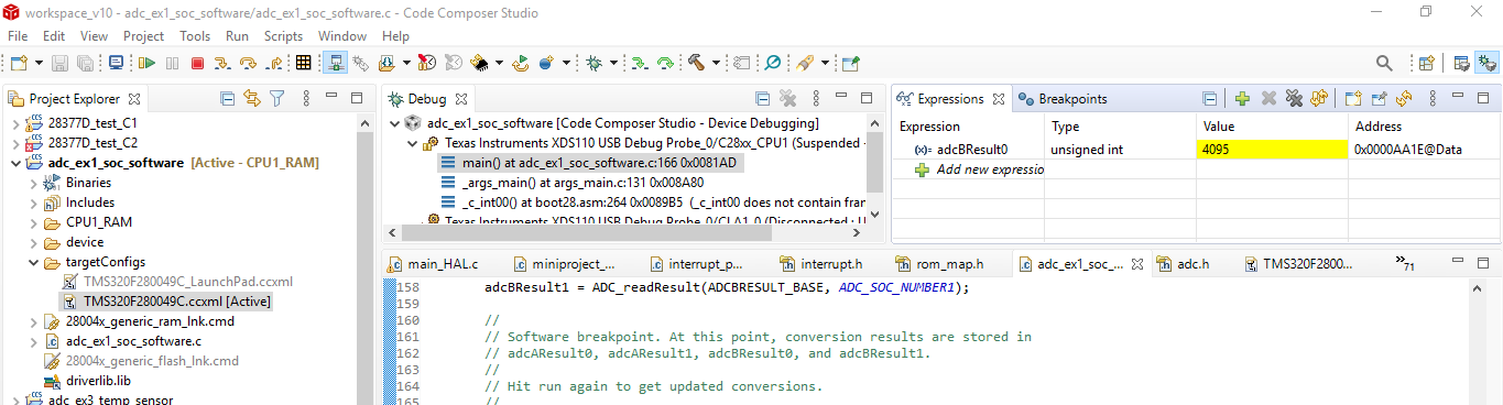
"C2000ware_2_00_00_02/driverlib/f28004x/examples/adc/adc_ex1_soc_software"
"C2000ware_2_00_00_02/driverlib/f28004x/examples/adc/adc_ex2_soc_epwm"
"C2000ware_2_00_00_02/driverlib/f28004x/examples/adc/adc_ex3_temp_sensor"
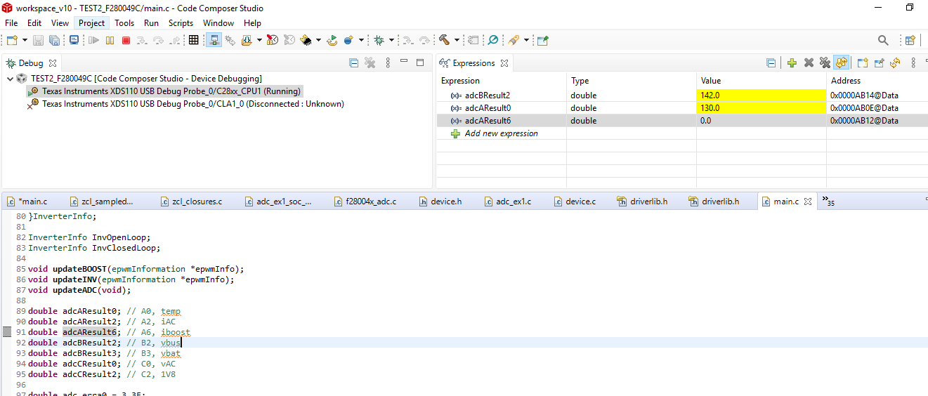
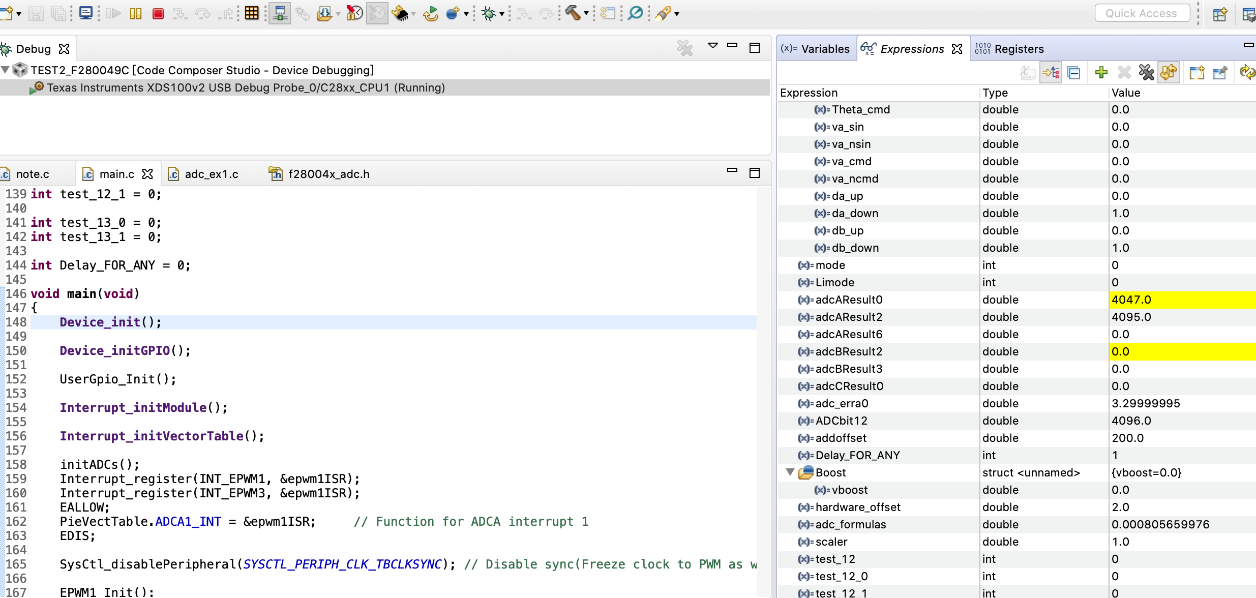
讀取的值會有亂跳的現象,以及當我同時使用ADCA, ADCB, ADCC BASE 會有一些通道並沒有辦法讀取資料
可否請教有人可以教教我讀取ADC
程式碼如下:
void initADCs(void)
{
//
// Setup VREF as internal
//
ADC_setVREF(ADCA_BASE, ADC_REFERENCE_INTERNAL, ADC_REFERENCE_3_3V);
ADC_setVREF(ADCB_BASE, ADC_REFERENCE_INTERNAL, ADC_REFERENCE_3_3V);
ADC_setVREF(ADCC_BASE, ADC_REFERENCE_INTERNAL, ADC_REFERENCE_3_3V);
//
// Set ADCCLK divider to /4
//
ADC_setPrescaler(ADCA_BASE, ADC_CLK_DIV_1_0);
ADC_setPrescaler(ADCB_BASE, ADC_CLK_DIV_1_0);
ADC_setPrescaler(ADCC_BASE, ADC_CLK_DIV_1_0);
//
// Set pulse positions to late
//
ADC_setInterruptPulseMode(ADCA_BASE, ADC_PULSE_END_OF_CONV);
ADC_setInterruptPulseMode(ADCB_BASE, ADC_PULSE_END_OF_CONV);
ADC_setInterruptPulseMode(ADCC_BASE, ADC_PULSE_END_OF_CONV);
//
// Power up the ADC and then delay for 1 ms
//
ADC_enableConverter(ADCA_BASE);
ADC_enableConverter(ADCB_BASE);
ADC_enableConverter(ADCC_BASE);
DEVICE_DELAY_US(1000);
}
void initADCSOCs(void)
{
//
// Configure SOC0 of ADCA to convert pin A0 with a sample window of 10
// SYSCLK cycles. The EPWM1SOCA signal will be the trigger.
//
ADC_setupSOC(ADCA_BASE, ADC_SOC_NUMBER0, ADC_TRIGGER_EPWM1_SOCA,
ADC_CH_ADCIN0, 10);
ADC_setupSOC(ADCA_BASE, ADC_SOC_NUMBER0, ADC_TRIGGER_EPWM1_SOCA,
ADC_CH_ADCIN2, 10);
//
// Set SOC1 to set the interrupt 1 flag. Enable the interrupt and make
// sure its flag is cleared.
//
ADC_setInterruptSource(ADCA_BASE, ADC_INT_NUMBER1, ADC_SOC_NUMBER1);
ADC_enableInterrupt(ADCA_BASE, ADC_INT_NUMBER1);
ADC_clearInterruptStatus(ADCA_BASE, ADC_INT_NUMBER1);
ADC_setupSOC(ADCB_BASE, ADC_SOC_NUMBER0, ADC_TRIGGER_EPWM1_SOCA,
ADC_CH_ADCIN2, 10);
ADC_setupSOC(ADCB_BASE, ADC_SOC_NUMBER0, ADC_TRIGGER_EPWM1_SOCA,
ADC_CH_ADCIN3, 10);
//
// Set SOC1 to set the interrupt 1 flag. Enable the interrupt and make
// sure its flag is cleared.
//
ADC_setInterruptSource(ADCB_BASE, ADC_INT_NUMBER1, ADC_SOC_NUMBER1);
ADC_enableInterrupt(ADCB_BASE, ADC_INT_NUMBER1);
ADC_clearInterruptStatus(ADCB_BASE, ADC_INT_NUMBER1);
}
ADC_forceSOC(ADCA_BASE, ADC_SOC_NUMBER0);
ADC_forceSOC(ADCA_BASE, ADC_SOC_NUMBER2);
ADC_forceSOC(ADCB_BASE, ADC_SOC_NUMBER2);
ADC_forceSOC(ADCB_BASE, ADC_SOC_NUMBER3);
ADC_forceSOC(ADCC_BASE, ADC_SOC_NUMBER4);
adcBResult3 = (AdcbResultRegs.ADCRESULT3);
for(Delay_FOR_ANY=0; Delay_FOR_ANY<1; Delay_FOR_ANY++){}
adcAResult0 = (AdcaResultRegs.ADCRESULT0);
for(Delay_FOR_ANY=0; Delay_FOR_ANY<1; Delay_FOR_ANY++){}
adcAResult2 = (AdcaResultRegs.ADCRESULT2);
for(Delay_FOR_ANY=0; Delay_FOR_ANY<1; Delay_FOR_ANY++){}
adcAResult6 = (AdcaResultRegs.ADCRESULT6);
for(Delay_FOR_ANY=0; Delay_FOR_ANY<1; Delay_FOR_ANY++){}
adcBResult2 = (AdcbResultRegs.ADCRESULT2);
for(Delay_FOR_ANY=0; Delay_FOR_ANY<1; Delay_FOR_ANY++){}
adcCResult0 = (AdccResultRegs.ADCRESULT0);
for(Delay_FOR_ANY=0; Delay_FOR_ANY<1; Delay_FOR_ANY++){}
adcCResult2 = (AdccResultRegs.ADCRESULT2);
for(Delay_FOR_ANY=0; Delay_FOR_ANY<1; Delay_FOR_ANY++){}
//AdcbRegs.ADCOFFTRIM.bit.OFFTRIM = addoffset;
adcAResult0 = ADC_readResult(ADCARESULT_BASE, ADC_SOC_NUMBER0);
adcAResult2 = ADC_readResult(ADCARESULT_BASE, ADC_SOC_NUMBER2);
adcAResult6 = ADC_readResult(ADCARESULT_BASE, ADC_SOC_NUMBER6);
adcBResult2 = ADC_readResult(ADCBRESULT_BASE, ADC_SOC_NUMBER2);
adcBResult3 = ADC_readResult(ADCBRESULT_BASE, ADC_SOC_NUMBER3);
adcCResult0 = ADC_readResult(ADCCRESULT_BASE, ADC_SOC_NUMBER0);
adcCResult2 = ADC_readResult(ADCCRESULT_BASE, ADC_SOC_NUMBER2);
PieCtrlRegs.PIEACK.all = PIEACK_GROUP1;