This thread has been locked.

If you have a related question, please click the "Ask a related question" button in the top right corner. The newly created question will be automatically linked to this question.

C2000 ware

Other Parts Discussed in Thread: C2000WARE

在测试自己DIY制作的电路板的过程中

发现232串口一直没有数据显示

1、自己思考可能出现的问题:

有可能是设计电路板的时候,232没有将RXD、TXD交叉连接

2、自己思考的解决方案:

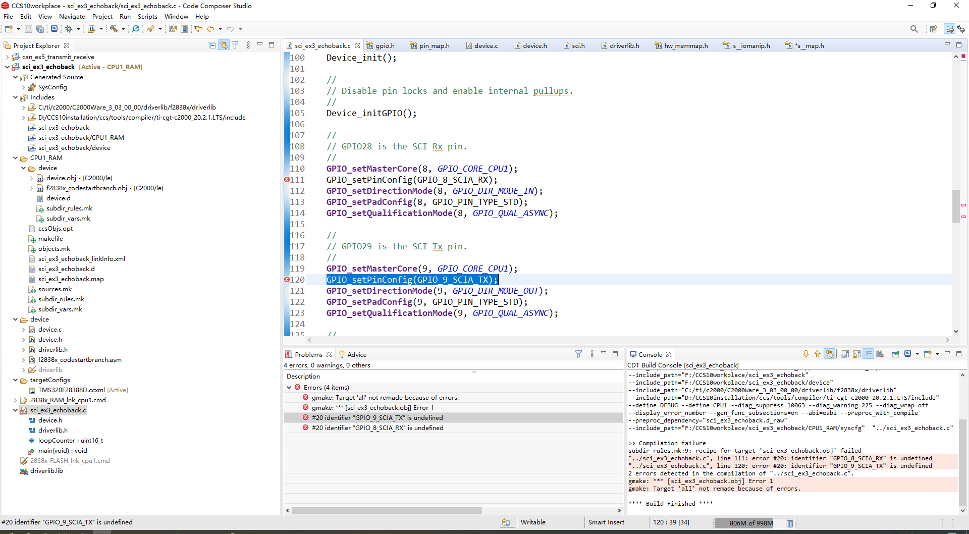
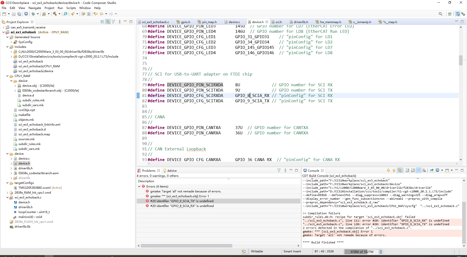
从CCS  C2000ware中的例程中,找到定义多路复用引脚的文件,将100多个引脚中的SCIA的功能定义,改成我们自己想要的功能。

3、操作如下:

例程初始定义的是

SCIA RXD是GPIO8 

SCIA TXD是GPIO9

我想修改成:

SCIA TXD是GPIO8 

SCIA RXD是GPIO9

4、相请教的问题

之前配置的时候,见过GPIOmap之类的文件,里面有何28388D的所有引脚的功能定义。

但是,现在单独去找,找了好久,没找到这个文件所在的位置

特来请教

谢谢

  • 您指的是下面的文件?

    //###########################################################################
    //
    // FILE:    f2838x_gpio.h
    //
    // TITLE:   Definitions for the GPIO registers.
    //
    //###########################################################################
    // $TI Release: F2838x Support Library v3.03.00.00 $
    // $Release Date: Sun Oct  4 16:00:36 IST 2020 $
    // $Copyright:
    // Copyright (C) 2020 Texas Instruments Incorporated - http://www.ti.com/
    //
    // Redistribution and use in source and binary forms, with or without 
    // modification, are permitted provided that the following conditions 
    // are met:
    // 
    //   Redistributions of source code must retain the above copyright 
    //   notice, this list of conditions and the following disclaimer.
    // 
    //   Redistributions in binary form must reproduce the above copyright
    //   notice, this list of conditions and the following disclaimer in the 
    //   documentation and/or other materials provided with the   
    //   distribution.
    // 
    //   Neither the name of Texas Instruments Incorporated nor the names of
    //   its contributors may be used to endorse or promote products derived
    //   from this software without specific prior written permission.
    // 
    // THIS SOFTWARE IS PROVIDED BY THE COPYRIGHT HOLDERS AND CONTRIBUTORS 
    // "AS IS" AND ANY EXPRESS OR IMPLIED WARRANTIES, INCLUDING, BUT NOT 
    // LIMITED TO, THE IMPLIED WARRANTIES OF MERCHANTABILITY AND FITNESS FOR
    // A PARTICULAR PURPOSE ARE DISCLAIMED. IN NO EVENT SHALL THE COPYRIGHT 
    // OWNER OR CONTRIBUTORS BE LIABLE FOR ANY DIRECT, INDIRECT, INCIDENTAL, 
    // SPECIAL, EXEMPLARY, OR CONSEQUENTIAL DAMAGES (INCLUDING, BUT NOT 
    // LIMITED TO, PROCUREMENT OF SUBSTITUTE GOODS OR SERVICES; LOSS OF USE,
    // DATA, OR PROFITS; OR BUSINESS INTERRUPTION) HOWEVER CAUSED AND ON ANY
    // THEORY OF LIABILITY, WHETHER IN CONTRACT, STRICT LIABILITY, OR TORT 
    // (INCLUDING NEGLIGENCE OR OTHERWISE) ARISING IN ANY WAY OUT OF THE USE 
    // OF THIS SOFTWARE, EVEN IF ADVISED OF THE POSSIBILITY OF SUCH DAMAGE.
    // $
    //###########################################################################
    
    #ifndef F2838X_GPIO_H
    #define F2838X_GPIO_H
    
    #ifdef __cplusplus
    extern "C" {
    #endif
    
    
    //---------------------------------------------------------------------------
    // GPIO Individual Register Bit Definitions:
    
    struct GPACTRL_BITS {                   // bits description
        Uint16 QUALPRD0:8;                  // 7:0 Qualification sampling period for GPIO0 to GPIO7
        Uint16 QUALPRD1:8;                  // 15:8 Qualification sampling period for GPIO8 to GPIO15
        Uint16 QUALPRD2:8;                  // 23:16 Qualification sampling period for GPIO16 to GPIO23
        Uint16 QUALPRD3:8;                  // 31:24 Qualification sampling period for GPIO24 to GPIO31
    };
    
    union GPACTRL_REG {
        Uint32  all;
        struct  GPACTRL_BITS  bit;
    };
    
    struct GPAQSEL1_BITS {                  // bits description
        Uint16 GPIO0:2;                     // 1:0 Select input qualification type for GPIO0
        Uint16 GPIO1:2;                     // 3:2 Select input qualification type for GPIO1
        Uint16 GPIO2:2;                     // 5:4 Select input qualification type for GPIO2
        Uint16 GPIO3:2;                     // 7:6 Select input qualification type for GPIO3
        Uint16 GPIO4:2;                     // 9:8 Select input qualification type for GPIO4
        Uint16 GPIO5:2;                     // 11:10 Select input qualification type for GPIO5
        Uint16 GPIO6:2;                     // 13:12 Select input qualification type for GPIO6
        Uint16 GPIO7:2;                     // 15:14 Select input qualification type for GPIO7
        Uint16 GPIO8:2;                     // 17:16 Select input qualification type for GPIO8
        Uint16 GPIO9:2;                     // 19:18 Select input qualification type for GPIO9
        Uint16 GPIO10:2;                    // 21:20 Select input qualification type for GPIO10
        Uint16 GPIO11:2;                    // 23:22 Select input qualification type for GPIO11
        Uint16 GPIO12:2;                    // 25:24 Select input qualification type for GPIO12
        Uint16 GPIO13:2;                    // 27:26 Select input qualification type for GPIO13
        Uint16 GPIO14:2;                    // 29:28 Select input qualification type for GPIO14
        Uint16 GPIO15:2;                    // 31:30 Select input qualification type for GPIO15
    };
    
    union GPAQSEL1_REG {
        Uint32  all;
        struct  GPAQSEL1_BITS  bit;
    };
    
    struct GPAQSEL2_BITS {                  // bits description
        Uint16 GPIO16:2;                    // 1:0 Select input qualification type for GPIO16
        Uint16 GPIO17:2;                    // 3:2 Select input qualification type for GPIO17
        Uint16 GPIO18:2;                    // 5:4 Select input qualification type for GPIO18
        Uint16 GPIO19:2;                    // 7:6 Select input qualification type for GPIO19
        Uint16 GPIO20:2;                    // 9:8 Select input qualification type for GPIO20
        Uint16 GPIO21:2;                    // 11:10 Select input qualification type for GPIO21
        Uint16 GPIO22:2;                    // 13:12 Select input qualification type for GPIO22
        Uint16 GPIO23:2;                    // 15:14 Select input qualification type for GPIO23
        Uint16 GPIO24:2;                    // 17:16 Select input qualification type for GPIO24
        Uint16 GPIO25:2;                    // 19:18 Select input qualification type for GPIO25
        Uint16 GPIO26:2;                    // 21:20 Select input qualification type for GPIO26
        Uint16 GPIO27:2;                    // 23:22 Select input qualification type for GPIO27
        Uint16 GPIO28:2;                    // 25:24 Select input qualification type for GPIO28
        Uint16 GPIO29:2;                    // 27:26 Select input qualification type for GPIO29
        Uint16 GPIO30:2;                    // 29:28 Select input qualification type for GPIO30
        Uint16 GPIO31:2;                    // 31:30 Select input qualification type for GPIO31
    };
    
    union GPAQSEL2_REG {
        Uint32  all;
        struct  GPAQSEL2_BITS  bit;
    };
    
    struct GPAMUX1_BITS {                   // bits description
        Uint16 GPIO0:2;                     // 1:0 Defines pin-muxing selection for GPIO0
        Uint16 GPIO1:2;                     // 3:2 Defines pin-muxing selection for GPIO1
        Uint16 GPIO2:2;                     // 5:4 Defines pin-muxing selection for GPIO2
        Uint16 GPIO3:2;                     // 7:6 Defines pin-muxing selection for GPIO3
        Uint16 GPIO4:2;                     // 9:8 Defines pin-muxing selection for GPIO4
        Uint16 GPIO5:2;                     // 11:10 Defines pin-muxing selection for GPIO5
        Uint16 GPIO6:2;                     // 13:12 Defines pin-muxing selection for GPIO6
        Uint16 GPIO7:2;                     // 15:14 Defines pin-muxing selection for GPIO7
        Uint16 GPIO8:2;                     // 17:16 Defines pin-muxing selection for GPIO8
        Uint16 GPIO9:2;                     // 19:18 Defines pin-muxing selection for GPIO9
        Uint16 GPIO10:2;                    // 21:20 Defines pin-muxing selection for GPIO10
        Uint16 GPIO11:2;                    // 23:22 Defines pin-muxing selection for GPIO11
        Uint16 GPIO12:2;                    // 25:24 Defines pin-muxing selection for GPIO12
        Uint16 GPIO13:2;                    // 27:26 Defines pin-muxing selection for GPIO13
        Uint16 GPIO14:2;                    // 29:28 Defines pin-muxing selection for GPIO14
        Uint16 GPIO15:2;                    // 31:30 Defines pin-muxing selection for GPIO15
    };
    
    union GPAMUX1_REG {
        Uint32  all;
        struct  GPAMUX1_BITS  bit;
    };
    
    struct GPAMUX2_BITS {                   // bits description
        Uint16 GPIO16:2;                    // 1:0 Defines pin-muxing selection for GPIO16
        Uint16 GPIO17:2;                    // 3:2 Defines pin-muxing selection for GPIO17
        Uint16 GPIO18:2;                    // 5:4 Defines pin-muxing selection for GPIO18
        Uint16 GPIO19:2;                    // 7:6 Defines pin-muxing selection for GPIO19
        Uint16 GPIO20:2;                    // 9:8 Defines pin-muxing selection for GPIO20
        Uint16 GPIO21:2;                    // 11:10 Defines pin-muxing selection for GPIO21
        Uint16 GPIO22:2;                    // 13:12 Defines pin-muxing selection for GPIO22
        Uint16 GPIO23:2;                    // 15:14 Defines pin-muxing selection for GPIO23
        Uint16 GPIO24:2;                    // 17:16 Defines pin-muxing selection for GPIO24
        Uint16 GPIO25:2;                    // 19:18 Defines pin-muxing selection for GPIO25
        Uint16 GPIO26:2;                    // 21:20 Defines pin-muxing selection for GPIO26
        Uint16 GPIO27:2;                    // 23:22 Defines pin-muxing selection for GPIO27
        Uint16 GPIO28:2;                    // 25:24 Defines pin-muxing selection for GPIO28
        Uint16 GPIO29:2;                    // 27:26 Defines pin-muxing selection for GPIO29
        Uint16 GPIO30:2;                    // 29:28 Defines pin-muxing selection for GPIO30
        Uint16 GPIO31:2;                    // 31:30 Defines pin-muxing selection for GPIO31
    };
    
    union GPAMUX2_REG {
        Uint32  all;
        struct  GPAMUX2_BITS  bit;
    };
    
    struct GPADIR_BITS {                    // bits description
        Uint16 GPIO0:1;                     // 0 Defines direction for this pin in GPIO mode
        Uint16 GPIO1:1;                     // 1 Defines direction for this pin in GPIO mode
        Uint16 GPIO2:1;                     // 2 Defines direction for this pin in GPIO mode
        Uint16 GPIO3:1;                     // 3 Defines direction for this pin in GPIO mode
        Uint16 GPIO4:1;                     // 4 Defines direction for this pin in GPIO mode
        Uint16 GPIO5:1;                     // 5 Defines direction for this pin in GPIO mode
        Uint16 GPIO6:1;                     // 6 Defines direction for this pin in GPIO mode
        Uint16 GPIO7:1;                     // 7 Defines direction for this pin in GPIO mode
        Uint16 GPIO8:1;                     // 8 Defines direction for this pin in GPIO mode
        Uint16 GPIO9:1;                     // 9 Defines direction for this pin in GPIO mode
        Uint16 GPIO10:1;                    // 10 Defines direction for this pin in GPIO mode
        Uint16 GPIO11:1;                    // 11 Defines direction for this pin in GPIO mode
        Uint16 GPIO12:1;                    // 12 Defines direction for this pin in GPIO mode
        Uint16 GPIO13:1;                    // 13 Defines direction for this pin in GPIO mode
        Uint16 GPIO14:1;                    // 14 Defines direction for this pin in GPIO mode
        Uint16 GPIO15:1;                    // 15 Defines direction for this pin in GPIO mode
        Uint16 GPIO16:1;                    // 16 Defines direction for this pin in GPIO mode
        Uint16 GPIO17:1;                    // 17 Defines direction for this pin in GPIO mode
        Uint16 GPIO18:1;                    // 18 Defines direction for this pin in GPIO mode
        Uint16 GPIO19:1;                    // 19 Defines direction for this pin in GPIO mode
        Uint16 GPIO20:1;                    // 20 Defines direction for this pin in GPIO mode
        Uint16 GPIO21:1;                    // 21 Defines direction for this pin in GPIO mode
        Uint16 GPIO22:1;                    // 22 Defines direction for this pin in GPIO mode
        Uint16 GPIO23:1;                    // 23 Defines direction for this pin in GPIO mode
        Uint16 GPIO24:1;                    // 24 Defines direction for this pin in GPIO mode
        Uint16 GPIO25:1;                    // 25 Defines direction for this pin in GPIO mode
        Uint16 GPIO26:1;                    // 26 Defines direction for this pin in GPIO mode
        Uint16 GPIO27:1;                    // 27 Defines direction for this pin in GPIO mode
        Uint16 GPIO28:1;                    // 28 Defines direction for this pin in GPIO mode
        Uint16 GPIO29:1;                    // 29 Defines direction for this pin in GPIO mode
        Uint16 GPIO30:1;                    // 30 Defines direction for this pin in GPIO mode
        Uint16 GPIO31:1;                    // 31 Defines direction for this pin in GPIO mode
    };
    
    union GPADIR_REG {
        Uint32  all;
        struct  GPADIR_BITS  bit;
    };
    
    struct GPAPUD_BITS {                    // bits description
        Uint16 GPIO0:1;                     // 0 Pull-Up Disable control for this pin
        Uint16 GPIO1:1;                     // 1 Pull-Up Disable control for this pin
        Uint16 GPIO2:1;                     // 2 Pull-Up Disable control for this pin
        Uint16 GPIO3:1;                     // 3 Pull-Up Disable control for this pin
        Uint16 GPIO4:1;                     // 4 Pull-Up Disable control for this pin
        Uint16 GPIO5:1;                     // 5 Pull-Up Disable control for this pin
        Uint16 GPIO6:1;                     // 6 Pull-Up Disable control for this pin
        Uint16 GPIO7:1;                     // 7 Pull-Up Disable control for this pin
        Uint16 GPIO8:1;                     // 8 Pull-Up Disable control for this pin
        Uint16 GPIO9:1;                     // 9 Pull-Up Disable control for this pin
        Uint16 GPIO10:1;                    // 10 Pull-Up Disable control for this pin
        Uint16 GPIO11:1;                    // 11 Pull-Up Disable control for this pin
        Uint16 GPIO12:1;                    // 12 Pull-Up Disable control for this pin
        Uint16 GPIO13:1;                    // 13 Pull-Up Disable control for this pin
        Uint16 GPIO14:1;                    // 14 Pull-Up Disable control for this pin
        Uint16 GPIO15:1;                    // 15 Pull-Up Disable control for this pin
        Uint16 GPIO16:1;                    // 16 Pull-Up Disable control for this pin
        Uint16 GPIO17:1;                    // 17 Pull-Up Disable control for this pin
        Uint16 GPIO18:1;                    // 18 Pull-Up Disable control for this pin
        Uint16 GPIO19:1;                    // 19 Pull-Up Disable control for this pin
        Uint16 GPIO20:1;                    // 20 Pull-Up Disable control for this pin
        Uint16 GPIO21:1;                    // 21 Pull-Up Disable control for this pin
        Uint16 GPIO22:1;                    // 22 Pull-Up Disable control for this pin
        Uint16 GPIO23:1;                    // 23 Pull-Up Disable control for this pin
        Uint16 GPIO24:1;                    // 24 Pull-Up Disable control for this pin
        Uint16 GPIO25:1;                    // 25 Pull-Up Disable control for this pin
        Uint16 GPIO26:1;                    // 26 Pull-Up Disable control for this pin
        Uint16 GPIO27:1;                    // 27 Pull-Up Disable control for this pin
        Uint16 GPIO28:1;                    // 28 Pull-Up Disable control for this pin
        Uint16 GPIO29:1;                    // 29 Pull-Up Disable control for this pin
        Uint16 GPIO30:1;                    // 30 Pull-Up Disable control for this pin
        Uint16 GPIO31:1;                    // 31 Pull-Up Disable control for this pin
    };
    
    union GPAPUD_REG {
        Uint32  all;
        struct  GPAPUD_BITS  bit;
    };
    
    struct GPAINV_BITS {                    // bits description
        Uint16 GPIO0:1;                     // 0 Input inversion control for this pin
        Uint16 GPIO1:1;                     // 1 Input inversion control for this pin
        Uint16 GPIO2:1;                     // 2 Input inversion control for this pin
        Uint16 GPIO3:1;                     // 3 Input inversion control for this pin
        Uint16 GPIO4:1;                     // 4 Input inversion control for this pin
        Uint16 GPIO5:1;                     // 5 Input inversion control for this pin
        Uint16 GPIO6:1;                     // 6 Input inversion control for this pin
        Uint16 GPIO7:1;                     // 7 Input inversion control for this pin
        Uint16 GPIO8:1;                     // 8 Input inversion control for this pin
        Uint16 GPIO9:1;                     // 9 Input inversion control for this pin
        Uint16 GPIO10:1;                    // 10 Input inversion control for this pin
        Uint16 GPIO11:1;                    // 11 Input inversion control for this pin
        Uint16 GPIO12:1;                    // 12 Input inversion control for this pin
        Uint16 GPIO13:1;                    // 13 Input inversion control for this pin
        Uint16 GPIO14:1;                    // 14 Input inversion control for this pin
        Uint16 GPIO15:1;                    // 15 Input inversion control for this pin
        Uint16 GPIO16:1;                    // 16 Input inversion control for this pin
        Uint16 GPIO17:1;                    // 17 Input inversion control for this pin
        Uint16 GPIO18:1;                    // 18 Input inversion control for this pin
        Uint16 GPIO19:1;                    // 19 Input inversion control for this pin
        Uint16 GPIO20:1;                    // 20 Input inversion control for this pin
        Uint16 GPIO21:1;                    // 21 Input inversion control for this pin
        Uint16 GPIO22:1;                    // 22 Input inversion control for this pin
        Uint16 GPIO23:1;                    // 23 Input inversion control for this pin
        Uint16 GPIO24:1;                    // 24 Input inversion control for this pin
        Uint16 GPIO25:1;                    // 25 Input inversion control for this pin
        Uint16 GPIO26:1;                    // 26 Input inversion control for this pin
        Uint16 GPIO27:1;                    // 27 Input inversion control for this pin
        Uint16 GPIO28:1;                    // 28 Input inversion control for this pin
        Uint16 GPIO29:1;                    // 29 Input inversion control for this pin
        Uint16 GPIO30:1;                    // 30 Input inversion control for this pin
        Uint16 GPIO31:1;                    // 31 Input inversion control for this pin
    };
    
    union GPAINV_REG {
        Uint32  all;
        struct  GPAINV_BITS  bit;
    };
    
    struct GPAODR_BITS {                    // bits description
        Uint16 GPIO0:1;                     // 0 Outpout Open-Drain control for this pin
        Uint16 GPIO1:1;                     // 1 Outpout Open-Drain control for this pin
        Uint16 GPIO2:1;                     // 2 Outpout Open-Drain control for this pin
        Uint16 GPIO3:1;                     // 3 Outpout Open-Drain control for this pin
        Uint16 GPIO4:1;                     // 4 Outpout Open-Drain control for this pin
        Uint16 GPIO5:1;                     // 5 Outpout Open-Drain control for this pin
        Uint16 GPIO6:1;                     // 6 Outpout Open-Drain control for this pin
        Uint16 GPIO7:1;                     // 7 Outpout Open-Drain control for this pin
        Uint16 GPIO8:1;                     // 8 Outpout Open-Drain control for this pin
        Uint16 GPIO9:1;                     // 9 Outpout Open-Drain control for this pin
        Uint16 GPIO10:1;                    // 10 Outpout Open-Drain control for this pin
        Uint16 GPIO11:1;                    // 11 Outpout Open-Drain control for this pin
        Uint16 GPIO12:1;                    // 12 Outpout Open-Drain control for this pin
        Uint16 GPIO13:1;                    // 13 Outpout Open-Drain control for this pin
        Uint16 GPIO14:1;                    // 14 Outpout Open-Drain control for this pin
        Uint16 GPIO15:1;                    // 15 Outpout Open-Drain control for this pin
        Uint16 GPIO16:1;                    // 16 Outpout Open-Drain control for this pin
        Uint16 GPIO17:1;                    // 17 Outpout Open-Drain control for this pin
        Uint16 GPIO18:1;                    // 18 Outpout Open-Drain control for this pin
        Uint16 GPIO19:1;                    // 19 Outpout Open-Drain control for this pin
        Uint16 GPIO20:1;                    // 20 Outpout Open-Drain control for this pin
        Uint16 GPIO21:1;                    // 21 Outpout Open-Drain control for this pin
        Uint16 GPIO22:1;                    // 22 Outpout Open-Drain control for this pin
        Uint16 GPIO23:1;                    // 23 Outpout Open-Drain control for this pin
        Uint16 GPIO24:1;                    // 24 Outpout Open-Drain control for this pin
        Uint16 GPIO25:1;                    // 25 Outpout Open-Drain control for this pin
        Uint16 GPIO26:1;                    // 26 Outpout Open-Drain control for this pin
        Uint16 GPIO27:1;                    // 27 Outpout Open-Drain control for this pin
        Uint16 GPIO28:1;                    // 28 Outpout Open-Drain control for this pin
        Uint16 GPIO29:1;                    // 29 Outpout Open-Drain control for this pin
        Uint16 GPIO30:1;                    // 30 Outpout Open-Drain control for this pin
        Uint16 GPIO31:1;                    // 31 Outpout Open-Drain control for this pin
    };
    
    union GPAODR_REG {
        Uint32  all;
        struct  GPAODR_BITS  bit;
    };
    
    struct GPAGMUX1_BITS {                  // bits description
        Uint16 GPIO0:2;                     // 1:0 Defines pin-muxing selection for GPIO0
        Uint16 GPIO1:2;                     // 3:2 Defines pin-muxing selection for GPIO1
        Uint16 GPIO2:2;                     // 5:4 Defines pin-muxing selection for GPIO2
        Uint16 GPIO3:2;                     // 7:6 Defines pin-muxing selection for GPIO3
        Uint16 GPIO4:2;                     // 9:8 Defines pin-muxing selection for GPIO4
        Uint16 GPIO5:2;                     // 11:10 Defines pin-muxing selection for GPIO5
        Uint16 GPIO6:2;                     // 13:12 Defines pin-muxing selection for GPIO6
        Uint16 GPIO7:2;                     // 15:14 Defines pin-muxing selection for GPIO7
        Uint16 GPIO8:2;                     // 17:16 Defines pin-muxing selection for GPIO8
        Uint16 GPIO9:2;                     // 19:18 Defines pin-muxing selection for GPIO9
        Uint16 GPIO10:2;                    // 21:20 Defines pin-muxing selection for GPIO10
        Uint16 GPIO11:2;                    // 23:22 Defines pin-muxing selection for GPIO11
        Uint16 GPIO12:2;                    // 25:24 Defines pin-muxing selection for GPIO12
        Uint16 GPIO13:2;                    // 27:26 Defines pin-muxing selection for GPIO13
        Uint16 GPIO14:2;                    // 29:28 Defines pin-muxing selection for GPIO14
        Uint16 GPIO15:2;                    // 31:30 Defines pin-muxing selection for GPIO15
    };
    
    union GPAGMUX1_REG {
        Uint32  all;
        struct  GPAGMUX1_BITS  bit;
    };
    
    struct GPAGMUX2_BITS {                  // bits description
        Uint16 GPIO16:2;                    // 1:0 Defines pin-muxing selection for GPIO16
        Uint16 GPIO17:2;                    // 3:2 Defines pin-muxing selection for GPIO17
        Uint16 GPIO18:2;                    // 5:4 Defines pin-muxing selection for GPIO18
        Uint16 GPIO19:2;                    // 7:6 Defines pin-muxing selection for GPIO19
        Uint16 GPIO20:2;                    // 9:8 Defines pin-muxing selection for GPIO20
        Uint16 GPIO21:2;                    // 11:10 Defines pin-muxing selection for GPIO21
        Uint16 GPIO22:2;                    // 13:12 Defines pin-muxing selection for GPIO22
        Uint16 GPIO23:2;                    // 15:14 Defines pin-muxing selection for GPIO23
        Uint16 GPIO24:2;                    // 17:16 Defines pin-muxing selection for GPIO24
        Uint16 GPIO25:2;                    // 19:18 Defines pin-muxing selection for GPIO25
        Uint16 GPIO26:2;                    // 21:20 Defines pin-muxing selection for GPIO26
        Uint16 GPIO27:2;                    // 23:22 Defines pin-muxing selection for GPIO27
        Uint16 GPIO28:2;                    // 25:24 Defines pin-muxing selection for GPIO28
        Uint16 GPIO29:2;                    // 27:26 Defines pin-muxing selection for GPIO29
        Uint16 GPIO30:2;                    // 29:28 Defines pin-muxing selection for GPIO30
        Uint16 GPIO31:2;                    // 31:30 Defines pin-muxing selection for GPIO31
    };
    
    union GPAGMUX2_REG {
        Uint32  all;
        struct  GPAGMUX2_BITS  bit;
    };
    
    struct GPACSEL1_BITS {                  // bits description
        Uint16 GPIO0:4;                     // 3:0 GPIO0 Master CPU Select
        Uint16 GPIO1:4;                     // 7:4 GPIO1 Master CPU Select
        Uint16 GPIO2:4;                     // 11:8 GPIO2 Master CPU Select
        Uint16 GPIO3:4;                     // 15:12 GPIO3 Master CPU Select
        Uint16 GPIO4:4;                     // 19:16 GPIO4 Master CPU Select
        Uint16 GPIO5:4;                     // 23:20 GPIO5 Master CPU Select
        Uint16 GPIO6:4;                     // 27:24 GPIO6 Master CPU Select
        Uint16 GPIO7:4;                     // 31:28 GPIO7 Master CPU Select
    };
    
    union GPACSEL1_REG {
        Uint32  all;
        struct  GPACSEL1_BITS  bit;
    };
    
    struct GPACSEL2_BITS {                  // bits description
        Uint16 GPIO8:4;                     // 3:0 GPIO8 Master CPU Select
        Uint16 GPIO9:4;                     // 7:4 GPIO9 Master CPU Select
        Uint16 GPIO10:4;                    // 11:8 GPIO10 Master CPU Select
        Uint16 GPIO11:4;                    // 15:12 GPIO11 Master CPU Select
        Uint16 GPIO12:4;                    // 19:16 GPIO12 Master CPU Select
        Uint16 GPIO13:4;                    // 23:20 GPIO13 Master CPU Select
        Uint16 GPIO14:4;                    // 27:24 GPIO14 Master CPU Select
        Uint16 GPIO15:4;                    // 31:28 GPIO15 Master CPU Select
    };
    
    union GPACSEL2_REG {
        Uint32  all;
        struct  GPACSEL2_BITS  bit;
    };
    
    struct GPACSEL3_BITS {                  // bits description
        Uint16 GPIO16:4;                    // 3:0 GPIO16 Master CPU Select
        Uint16 GPIO17:4;                    // 7:4 GPIO17 Master CPU Select
        Uint16 GPIO18:4;                    // 11:8 GPIO18 Master CPU Select
        Uint16 GPIO19:4;                    // 15:12 GPIO19 Master CPU Select
        Uint16 GPIO20:4;                    // 19:16 GPIO20 Master CPU Select
        Uint16 GPIO21:4;                    // 23:20 GPIO21 Master CPU Select
        Uint16 GPIO22:4;                    // 27:24 GPIO22 Master CPU Select
        Uint16 GPIO23:4;                    // 31:28 GPIO23 Master CPU Select
    };
    
    union GPACSEL3_REG {
        Uint32  all;
        struct  GPACSEL3_BITS  bit;
    };
    
    struct GPACSEL4_BITS {                  // bits description
        Uint16 GPIO24:4;                    // 3:0 GPIO24 Master CPU Select
        Uint16 GPIO25:4;                    // 7:4 GPIO25 Master CPU Select
        Uint16 GPIO26:4;                    // 11:8 GPIO26 Master CPU Select
        Uint16 GPIO27:4;                    // 15:12 GPIO27 Master CPU Select
        Uint16 GPIO28:4;                    // 19:16 GPIO28 Master CPU Select
        Uint16 GPIO29:4;                    // 23:20 GPIO29 Master CPU Select
        Uint16 GPIO30:4;                    // 27:24 GPIO30 Master CPU Select
        Uint16 GPIO31:4;                    // 31:28 GPIO31 Master CPU Select
    };
    
    union GPACSEL4_REG {
        Uint32  all;
        struct  GPACSEL4_BITS  bit;
    };
    
    struct GPALOCK_BITS {                   // bits description
        Uint16 GPIO0:1;                     // 0 Configuration Lock bit for this pin
        Uint16 GPIO1:1;                     // 1 Configuration Lock bit for this pin
        Uint16 GPIO2:1;                     // 2 Configuration Lock bit for this pin
        Uint16 GPIO3:1;                     // 3 Configuration Lock bit for this pin
        Uint16 GPIO4:1;                     // 4 Configuration Lock bit for this pin
        Uint16 GPIO5:1;                     // 5 Configuration Lock bit for this pin
        Uint16 GPIO6:1;                     // 6 Configuration Lock bit for this pin
        Uint16 GPIO7:1;                     // 7 Configuration Lock bit for this pin
        Uint16 GPIO8:1;                     // 8 Configuration Lock bit for this pin
        Uint16 GPIO9:1;                     // 9 Configuration Lock bit for this pin
        Uint16 GPIO10:1;                    // 10 Configuration Lock bit for this pin
        Uint16 GPIO11:1;                    // 11 Configuration Lock bit for this pin
        Uint16 GPIO12:1;                    // 12 Configuration Lock bit for this pin
        Uint16 GPIO13:1;                    // 13 Configuration Lock bit for this pin
        Uint16 GPIO14:1;                    // 14 Configuration Lock bit for this pin
        Uint16 GPIO15:1;                    // 15 Configuration Lock bit for this pin
        Uint16 GPIO16:1;                    // 16 Configuration Lock bit for this pin
        Uint16 GPIO17:1;                    // 17 Configuration Lock bit for this pin
        Uint16 GPIO18:1;                    // 18 Configuration Lock bit for this pin
        Uint16 GPIO19:1;                    // 19 Configuration Lock bit for this pin
        Uint16 GPIO20:1;                    // 20 Configuration Lock bit for this pin
        Uint16 GPIO21:1;                    // 21 Configuration Lock bit for this pin
        Uint16 GPIO22:1;                    // 22 Configuration Lock bit for this pin
        Uint16 GPIO23:1;                    // 23 Configuration Lock bit for this pin
        Uint16 GPIO24:1;                    // 24 Configuration Lock bit for this pin
        Uint16 GPIO25:1;                    // 25 Configuration Lock bit for this pin
        Uint16 GPIO26:1;                    // 26 Configuration Lock bit for this pin
        Uint16 GPIO27:1;                    // 27 Configuration Lock bit for this pin
        Uint16 GPIO28:1;                    // 28 Configuration Lock bit for this pin
        Uint16 GPIO29:1;                    // 29 Configuration Lock bit for this pin
        Uint16 GPIO30:1;                    // 30 Configuration Lock bit for this pin
        Uint16 GPIO31:1;                    // 31 Configuration Lock bit for this pin
    };
    
    union GPALOCK_REG {
        Uint32  all;
        struct  GPALOCK_BITS  bit;
    };
    
    struct GPACR_BITS {                     // bits description
        Uint16 GPIO0:1;                     // 0 Configuration lock commit bit for this pin
        Uint16 GPIO1:1;                     // 1 Configuration lock commit bit for this pin
        Uint16 GPIO2:1;                     // 2 Configuration lock commit bit for this pin
        Uint16 GPIO3:1;                     // 3 Configuration lock commit bit for this pin
        Uint16 GPIO4:1;                     // 4 Configuration lock commit bit for this pin
        Uint16 GPIO5:1;                     // 5 Configuration lock commit bit for this pin
        Uint16 GPIO6:1;                     // 6 Configuration lock commit bit for this pin
        Uint16 GPIO7:1;                     // 7 Configuration lock commit bit for this pin
        Uint16 GPIO8:1;                     // 8 Configuration lock commit bit for this pin
        Uint16 GPIO9:1;                     // 9 Configuration lock commit bit for this pin
        Uint16 GPIO10:1;                    // 10 Configuration lock commit bit for this pin
        Uint16 GPIO11:1;                    // 11 Configuration lock commit bit for this pin
        Uint16 GPIO12:1;                    // 12 Configuration lock commit bit for this pin
        Uint16 GPIO13:1;                    // 13 Configuration lock commit bit for this pin
        Uint16 GPIO14:1;                    // 14 Configuration lock commit bit for this pin
        Uint16 GPIO15:1;                    // 15 Configuration lock commit bit for this pin
        Uint16 GPIO16:1;                    // 16 Configuration lock commit bit for this pin
        Uint16 GPIO17:1;                    // 17 Configuration lock commit bit for this pin
        Uint16 GPIO18:1;                    // 18 Configuration lock commit bit for this pin
        Uint16 GPIO19:1;                    // 19 Configuration lock commit bit for this pin
        Uint16 GPIO20:1;                    // 20 Configuration lock commit bit for this pin
        Uint16 GPIO21:1;                    // 21 Configuration lock commit bit for this pin
        Uint16 GPIO22:1;                    // 22 Configuration lock commit bit for this pin
        Uint16 GPIO23:1;                    // 23 Configuration lock commit bit for this pin
        Uint16 GPIO24:1;                    // 24 Configuration lock commit bit for this pin
        Uint16 GPIO25:1;                    // 25 Configuration lock commit bit for this pin
        Uint16 GPIO26:1;                    // 26 Configuration lock commit bit for this pin
        Uint16 GPIO27:1;                    // 27 Configuration lock commit bit for this pin
        Uint16 GPIO28:1;                    // 28 Configuration lock commit bit for this pin
        Uint16 GPIO29:1;                    // 29 Configuration lock commit bit for this pin
        Uint16 GPIO30:1;                    // 30 Configuration lock commit bit for this pin
        Uint16 GPIO31:1;                    // 31 Configuration lock commit bit for this pin
    };
    
    union GPACR_REG {
        Uint32  all;
        struct  GPACR_BITS  bit;
    };
    
    struct GPBCTRL_BITS {                   // bits description
        Uint16 QUALPRD0:8;                  // 7:0 Qualification sampling period for GPIO32 to GPIO39
        Uint16 QUALPRD1:8;                  // 15:8 Qualification sampling period for GPIO40 to GPIO47
        Uint16 QUALPRD2:8;                  // 23:16 Qualification sampling period for GPIO48 to GPIO55
        Uint16 QUALPRD3:8;                  // 31:24 Qualification sampling period for GPIO56 to GPIO63
    };
    
    union GPBCTRL_REG {
        Uint32  all;
        struct  GPBCTRL_BITS  bit;
    };
    
    struct GPBQSEL1_BITS {                  // bits description
        Uint16 GPIO32:2;                    // 1:0 Select input qualification type for GPIO32
        Uint16 GPIO33:2;                    // 3:2 Select input qualification type for GPIO33
        Uint16 GPIO34:2;                    // 5:4 Select input qualification type for GPIO34
        Uint16 GPIO35:2;                    // 7:6 Select input qualification type for GPIO35
        Uint16 GPIO36:2;                    // 9:8 Select input qualification type for GPIO36
        Uint16 GPIO37:2;                    // 11:10 Select input qualification type for GPIO37
        Uint16 GPIO38:2;                    // 13:12 Select input qualification type for GPIO38
        Uint16 GPIO39:2;                    // 15:14 Select input qualification type for GPIO39
        Uint16 GPIO40:2;                    // 17:16 Select input qualification type for GPIO40
        Uint16 GPIO41:2;                    // 19:18 Select input qualification type for GPIO41
        Uint16 GPIO42:2;                    // 21:20 Select input qualification type for GPIO42
        Uint16 GPIO43:2;                    // 23:22 Select input qualification type for GPIO43
        Uint16 GPIO44:2;                    // 25:24 Select input qualification type for GPIO44
        Uint16 GPIO45:2;                    // 27:26 Select input qualification type for GPIO45
        Uint16 GPIO46:2;                    // 29:28 Select input qualification type for GPIO46
        Uint16 GPIO47:2;                    // 31:30 Select input qualification type for GPIO47
    };
    
    union GPBQSEL1_REG {
        Uint32  all;
        struct  GPBQSEL1_BITS  bit;
    };
    
    struct GPBQSEL2_BITS {                  // bits description
        Uint16 GPIO48:2;                    // 1:0 Select input qualification type for GPIO48
        Uint16 GPIO49:2;                    // 3:2 Select input qualification type for GPIO49
        Uint16 GPIO50:2;                    // 5:4 Select input qualification type for GPIO50
        Uint16 GPIO51:2;                    // 7:6 Select input qualification type for GPIO51
        Uint16 GPIO52:2;                    // 9:8 Select input qualification type for GPIO52
        Uint16 GPIO53:2;                    // 11:10 Select input qualification type for GPIO53
        Uint16 GPIO54:2;                    // 13:12 Select input qualification type for GPIO54
        Uint16 GPIO55:2;                    // 15:14 Select input qualification type for GPIO55
        Uint16 GPIO56:2;                    // 17:16 Select input qualification type for GPIO56
        Uint16 GPIO57:2;                    // 19:18 Select input qualification type for GPIO57
        Uint16 GPIO58:2;                    // 21:20 Select input qualification type for GPIO58
        Uint16 GPIO59:2;                    // 23:22 Select input qualification type for GPIO59
        Uint16 GPIO60:2;                    // 25:24 Select input qualification type for GPIO60
        Uint16 GPIO61:2;                    // 27:26 Select input qualification type for GPIO61
        Uint16 GPIO62:2;                    // 29:28 Select input qualification type for GPIO62
        Uint16 GPIO63:2;                    // 31:30 Select input qualification type for GPIO63
    };
    
    union GPBQSEL2_REG {
        Uint32  all;
        struct  GPBQSEL2_BITS  bit;
    };
    
    struct GPBMUX1_BITS {                   // bits description
        Uint16 GPIO32:2;                    // 1:0 Defines pin-muxing selection for GPIO32
        Uint16 GPIO33:2;                    // 3:2 Defines pin-muxing selection for GPIO33
        Uint16 GPIO34:2;                    // 5:4 Defines pin-muxing selection for GPIO34
        Uint16 GPIO35:2;                    // 7:6 Defines pin-muxing selection for GPIO35
        Uint16 GPIO36:2;                    // 9:8 Defines pin-muxing selection for GPIO36
        Uint16 GPIO37:2;                    // 11:10 Defines pin-muxing selection for GPIO37
        Uint16 GPIO38:2;                    // 13:12 Defines pin-muxing selection for GPIO38
        Uint16 GPIO39:2;                    // 15:14 Defines pin-muxing selection for GPIO39
        Uint16 GPIO40:2;                    // 17:16 Defines pin-muxing selection for GPIO40
        Uint16 GPIO41:2;                    // 19:18 Defines pin-muxing selection for GPIO41
        Uint16 GPIO42:2;                    // 21:20 Defines pin-muxing selection for GPIO42
        Uint16 GPIO43:2;                    // 23:22 Defines pin-muxing selection for GPIO43
        Uint16 GPIO44:2;                    // 25:24 Defines pin-muxing selection for GPIO44
        Uint16 GPIO45:2;                    // 27:26 Defines pin-muxing selection for GPIO45
        Uint16 GPIO46:2;                    // 29:28 Defines pin-muxing selection for GPIO46
        Uint16 GPIO47:2;                    // 31:30 Defines pin-muxing selection for GPIO47
    };
    
    union GPBMUX1_REG {
        Uint32  all;
        struct  GPBMUX1_BITS  bit;
    };
    
    struct GPBMUX2_BITS {                   // bits description
        Uint16 GPIO48:2;                    // 1:0 Defines pin-muxing selection for GPIO48
        Uint16 GPIO49:2;                    // 3:2 Defines pin-muxing selection for GPIO49
        Uint16 GPIO50:2;                    // 5:4 Defines pin-muxing selection for GPIO50
        Uint16 GPIO51:2;                    // 7:6 Defines pin-muxing selection for GPIO51
        Uint16 GPIO52:2;                    // 9:8 Defines pin-muxing selection for GPIO52
        Uint16 GPIO53:2;                    // 11:10 Defines pin-muxing selection for GPIO53
        Uint16 GPIO54:2;                    // 13:12 Defines pin-muxing selection for GPIO54
        Uint16 GPIO55:2;                    // 15:14 Defines pin-muxing selection for GPIO55
        Uint16 GPIO56:2;                    // 17:16 Defines pin-muxing selection for GPIO56
        Uint16 GPIO57:2;                    // 19:18 Defines pin-muxing selection for GPIO57
        Uint16 GPIO58:2;                    // 21:20 Defines pin-muxing selection for GPIO58
        Uint16 GPIO59:2;                    // 23:22 Defines pin-muxing selection for GPIO59
        Uint16 GPIO60:2;                    // 25:24 Defines pin-muxing selection for GPIO60
        Uint16 GPIO61:2;                    // 27:26 Defines pin-muxing selection for GPIO61
        Uint16 GPIO62:2;                    // 29:28 Defines pin-muxing selection for GPIO62
        Uint16 GPIO63:2;                    // 31:30 Defines pin-muxing selection for GPIO63
    };
    
    union GPBMUX2_REG {
        Uint32  all;
        struct  GPBMUX2_BITS  bit;
    };
    
    struct GPBDIR_BITS {                    // bits description
        Uint16 GPIO32:1;                    // 0 Defines direction for this pin in GPIO mode
        Uint16 GPIO33:1;                    // 1 Defines direction for this pin in GPIO mode
        Uint16 GPIO34:1;                    // 2 Defines direction for this pin in GPIO mode
        Uint16 GPIO35:1;                    // 3 Defines direction for this pin in GPIO mode
        Uint16 GPIO36:1;                    // 4 Defines direction for this pin in GPIO mode
        Uint16 GPIO37:1;                    // 5 Defines direction for this pin in GPIO mode
        Uint16 GPIO38:1;                    // 6 Defines direction for this pin in GPIO mode
        Uint16 GPIO39:1;                    // 7 Defines direction for this pin in GPIO mode
        Uint16 GPIO40:1;                    // 8 Defines direction for this pin in GPIO mode
        Uint16 GPIO41:1;                    // 9 Defines direction for this pin in GPIO mode
        Uint16 GPIO42:1;                    // 10 Defines direction for this pin in GPIO mode
        Uint16 GPIO43:1;                    // 11 Defines direction for this pin in GPIO mode
        Uint16 GPIO44:1;                    // 12 Defines direction for this pin in GPIO mode
        Uint16 GPIO45:1;                    // 13 Defines direction for this pin in GPIO mode
        Uint16 GPIO46:1;                    // 14 Defines direction for this pin in GPIO mode
        Uint16 GPIO47:1;                    // 15 Defines direction for this pin in GPIO mode
        Uint16 GPIO48:1;                    // 16 Defines direction for this pin in GPIO mode
        Uint16 GPIO49:1;                    // 17 Defines direction for this pin in GPIO mode
        Uint16 GPIO50:1;                    // 18 Defines direction for this pin in GPIO mode
        Uint16 GPIO51:1;                    // 19 Defines direction for this pin in GPIO mode
        Uint16 GPIO52:1;                    // 20 Defines direction for this pin in GPIO mode
        Uint16 GPIO53:1;                    // 21 Defines direction for this pin in GPIO mode
        Uint16 GPIO54:1;                    // 22 Defines direction for this pin in GPIO mode
        Uint16 GPIO55:1;                    // 23 Defines direction for this pin in GPIO mode
        Uint16 GPIO56:1;                    // 24 Defines direction for this pin in GPIO mode
        Uint16 GPIO57:1;                    // 25 Defines direction for this pin in GPIO mode
        Uint16 GPIO58:1;                    // 26 Defines direction for this pin in GPIO mode
        Uint16 GPIO59:1;                    // 27 Defines direction for this pin in GPIO mode
        Uint16 GPIO60:1;                    // 28 Defines direction for this pin in GPIO mode
        Uint16 GPIO61:1;                    // 29 Defines direction for this pin in GPIO mode
        Uint16 GPIO62:1;                    // 30 Defines direction for this pin in GPIO mode
        Uint16 GPIO63:1;                    // 31 Defines direction for this pin in GPIO mode
    };
    
    union GPBDIR_REG {
        Uint32  all;
        struct  GPBDIR_BITS  bit;
    };
    
    struct GPBPUD_BITS {                    // bits description
        Uint16 GPIO32:1;                    // 0 Pull-Up Disable control for this pin
        Uint16 GPIO33:1;                    // 1 Pull-Up Disable control for this pin
        Uint16 GPIO34:1;                    // 2 Pull-Up Disable control for this pin
        Uint16 GPIO35:1;                    // 3 Pull-Up Disable control for this pin
        Uint16 GPIO36:1;                    // 4 Pull-Up Disable control for this pin
        Uint16 GPIO37:1;                    // 5 Pull-Up Disable control for this pin
        Uint16 GPIO38:1;                    // 6 Pull-Up Disable control for this pin
        Uint16 GPIO39:1;                    // 7 Pull-Up Disable control for this pin
        Uint16 GPIO40:1;                    // 8 Pull-Up Disable control for this pin
        Uint16 GPIO41:1;                    // 9 Pull-Up Disable control for this pin
        Uint16 GPIO42:1;                    // 10 Pull-Up Disable control for this pin
        Uint16 GPIO43:1;                    // 11 Pull-Up Disable control for this pin
        Uint16 GPIO44:1;                    // 12 Pull-Up Disable control for this pin
        Uint16 GPIO45:1;                    // 13 Pull-Up Disable control for this pin
        Uint16 GPIO46:1;                    // 14 Pull-Up Disable control for this pin
        Uint16 GPIO47:1;                    // 15 Pull-Up Disable control for this pin
        Uint16 GPIO48:1;                    // 16 Pull-Up Disable control for this pin
        Uint16 GPIO49:1;                    // 17 Pull-Up Disable control for this pin
        Uint16 GPIO50:1;                    // 18 Pull-Up Disable control for this pin
        Uint16 GPIO51:1;                    // 19 Pull-Up Disable control for this pin
        Uint16 GPIO52:1;                    // 20 Pull-Up Disable control for this pin
        Uint16 GPIO53:1;                    // 21 Pull-Up Disable control for this pin
        Uint16 GPIO54:1;                    // 22 Pull-Up Disable control for this pin
        Uint16 GPIO55:1;                    // 23 Pull-Up Disable control for this pin
        Uint16 GPIO56:1;                    // 24 Pull-Up Disable control for this pin
        Uint16 GPIO57:1;                    // 25 Pull-Up Disable control for this pin
        Uint16 GPIO58:1;                    // 26 Pull-Up Disable control for this pin
        Uint16 GPIO59:1;                    // 27 Pull-Up Disable control for this pin
        Uint16 GPIO60:1;                    // 28 Pull-Up Disable control for this pin
        Uint16 GPIO61:1;                    // 29 Pull-Up Disable control for this pin
        Uint16 GPIO62:1;                    // 30 Pull-Up Disable control for this pin
        Uint16 GPIO63:1;                    // 31 Pull-Up Disable control for this pin
    };
    
    union GPBPUD_REG {
        Uint32  all;
        struct  GPBPUD_BITS  bit;
    };
    
    struct GPBINV_BITS {                    // bits description
        Uint16 GPIO32:1;                    // 0 Input inversion control for this pin
        Uint16 GPIO33:1;                    // 1 Input inversion control for this pin
        Uint16 GPIO34:1;                    // 2 Input inversion control for this pin
        Uint16 GPIO35:1;                    // 3 Input inversion control for this pin
        Uint16 GPIO36:1;                    // 4 Input inversion control for this pin
        Uint16 GPIO37:1;                    // 5 Input inversion control for this pin
        Uint16 GPIO38:1;                    // 6 Input inversion control for this pin
        Uint16 GPIO39:1;                    // 7 Input inversion control for this pin
        Uint16 GPIO40:1;                    // 8 Input inversion control for this pin
        Uint16 GPIO41:1;                    // 9 Input inversion control for this pin
        Uint16 GPIO42:1;                    // 10 Input inversion control for this pin
        Uint16 GPIO43:1;                    // 11 Input inversion control for this pin
        Uint16 GPIO44:1;                    // 12 Input inversion control for this pin
        Uint16 GPIO45:1;                    // 13 Input inversion control for this pin
        Uint16 GPIO46:1;                    // 14 Input inversion control for this pin
        Uint16 GPIO47:1;                    // 15 Input inversion control for this pin
        Uint16 GPIO48:1;                    // 16 Input inversion control for this pin
        Uint16 GPIO49:1;                    // 17 Input inversion control for this pin
        Uint16 GPIO50:1;                    // 18 Input inversion control for this pin
        Uint16 GPIO51:1;                    // 19 Input inversion control for this pin
        Uint16 GPIO52:1;                    // 20 Input inversion control for this pin
        Uint16 GPIO53:1;                    // 21 Input inversion control for this pin
        Uint16 GPIO54:1;                    // 22 Input inversion control for this pin
        Uint16 GPIO55:1;                    // 23 Input inversion control for this pin
        Uint16 GPIO56:1;                    // 24 Input inversion control for this pin
        Uint16 GPIO57:1;                    // 25 Input inversion control for this pin
        Uint16 GPIO58:1;                    // 26 Input inversion control for this pin
        Uint16 GPIO59:1;                    // 27 Input inversion control for this pin
        Uint16 GPIO60:1;                    // 28 Input inversion control for this pin
        Uint16 GPIO61:1;                    // 29 Input inversion control for this pin
        Uint16 GPIO62:1;                    // 30 Input inversion control for this pin
        Uint16 GPIO63:1;                    // 31 Input inversion control for this pin
    };
    
    union GPBINV_REG {
        Uint32  all;
        struct  GPBINV_BITS  bit;
    };
    
    struct GPBODR_BITS {                    // bits description
        Uint16 GPIO32:1;                    // 0 Outpout Open-Drain control for this pin
        Uint16 GPIO33:1;                    // 1 Outpout Open-Drain control for this pin
        Uint16 GPIO34:1;                    // 2 Outpout Open-Drain control for this pin
        Uint16 GPIO35:1;                    // 3 Outpout Open-Drain control for this pin
        Uint16 GPIO36:1;                    // 4 Outpout Open-Drain control for this pin
        Uint16 GPIO37:1;                    // 5 Outpout Open-Drain control for this pin
        Uint16 GPIO38:1;                    // 6 Outpout Open-Drain control for this pin
        Uint16 GPIO39:1;                    // 7 Outpout Open-Drain control for this pin
        Uint16 GPIO40:1;                    // 8 Outpout Open-Drain control for this pin
        Uint16 GPIO41:1;                    // 9 Outpout Open-Drain control for this pin
        Uint16 GPIO42:1;                    // 10 Outpout Open-Drain control for this pin
        Uint16 GPIO43:1;                    // 11 Outpout Open-Drain control for this pin
        Uint16 GPIO44:1;                    // 12 Outpout Open-Drain control for this pin
        Uint16 GPIO45:1;                    // 13 Outpout Open-Drain control for this pin
        Uint16 GPIO46:1;                    // 14 Outpout Open-Drain control for this pin
        Uint16 GPIO47:1;                    // 15 Outpout Open-Drain control for this pin
        Uint16 GPIO48:1;                    // 16 Outpout Open-Drain control for this pin
        Uint16 GPIO49:1;                    // 17 Outpout Open-Drain control for this pin
        Uint16 GPIO50:1;                    // 18 Outpout Open-Drain control for this pin
        Uint16 GPIO51:1;                    // 19 Outpout Open-Drain control for this pin
        Uint16 GPIO52:1;                    // 20 Outpout Open-Drain control for this pin
        Uint16 GPIO53:1;                    // 21 Outpout Open-Drain control for this pin
        Uint16 GPIO54:1;                    // 22 Outpout Open-Drain control for this pin
        Uint16 GPIO55:1;                    // 23 Outpout Open-Drain control for this pin
        Uint16 GPIO56:1;                    // 24 Outpout Open-Drain control for this pin
        Uint16 GPIO57:1;                    // 25 Outpout Open-Drain control for this pin
        Uint16 GPIO58:1;                    // 26 Outpout Open-Drain control for this pin
        Uint16 GPIO59:1;                    // 27 Outpout Open-Drain control for this pin
        Uint16 GPIO60:1;                    // 28 Outpout Open-Drain control for this pin
        Uint16 GPIO61:1;                    // 29 Outpout Open-Drain control for this pin
        Uint16 GPIO62:1;                    // 30 Outpout Open-Drain control for this pin
        Uint16 GPIO63:1;                    // 31 Outpout Open-Drain control for this pin
    };
    
    union GPBODR_REG {
        Uint32  all;
        struct  GPBODR_BITS  bit;
    };
    
    struct GPBAMSEL_BITS {                  // bits description
        Uint16 rsvd1:1;                     // 0 Reserved
        Uint16 rsvd2:1;                     // 1 Reserved
        Uint16 rsvd3:1;                     // 2 Reserved
        Uint16 rsvd4:1;                     // 3 Reserved
        Uint16 rsvd5:1;                     // 4 Reserved
        Uint16 rsvd6:1;                     // 5 Reserved
        Uint16 rsvd7:1;                     // 6 Reserved
        Uint16 rsvd8:1;                     // 7 Reserved
        Uint16 rsvd9:1;                     // 8 Reserved
        Uint16 rsvd10:1;                    // 9 Reserved
        Uint16 GPIO42:1;                    // 10 Analog Mode select for this pin
        Uint16 GPIO43:1;                    // 11 Analog Mode select for this pin
        Uint16 rsvd11:1;                    // 12 Reserved
        Uint16 rsvd12:1;                    // 13 Reserved
        Uint16 rsvd13:1;                    // 14 Reserved
        Uint16 rsvd14:1;                    // 15 Reserved
        Uint16 rsvd15:1;                    // 16 Reserved
        Uint16 rsvd16:1;                    // 17 Reserved
        Uint16 rsvd17:1;                    // 18 Reserved
        Uint16 rsvd18:1;                    // 19 Reserved
        Uint16 rsvd19:1;                    // 20 Reserved
        Uint16 rsvd20:1;                    // 21 Reserved
        Uint16 rsvd21:1;                    // 22 Reserved
        Uint16 rsvd22:1;                    // 23 Reserved
        Uint16 rsvd23:1;                    // 24 Reserved
        Uint16 rsvd24:1;                    // 25 Reserved
        Uint16 rsvd25:1;                    // 26 Reserved
        Uint16 rsvd26:1;                    // 27 Reserved
        Uint16 rsvd27:1;                    // 28 Reserved
        Uint16 rsvd28:1;                    // 29 Reserved
        Uint16 rsvd29:1;                    // 30 Reserved
        Uint16 rsvd30:1;                    // 31 Reserved
    };
    
    union GPBAMSEL_REG {
        Uint32  all;
        struct  GPBAMSEL_BITS  bit;
    };
    
    struct GPBGMUX1_BITS {                  // bits description
        Uint16 GPIO32:2;                    // 1:0 Defines pin-muxing selection for GPIO32
        Uint16 GPIO33:2;                    // 3:2 Defines pin-muxing selection for GPIO33
        Uint16 GPIO34:2;                    // 5:4 Defines pin-muxing selection for GPIO34
        Uint16 GPIO35:2;                    // 7:6 Defines pin-muxing selection for GPIO35
        Uint16 GPIO36:2;                    // 9:8 Defines pin-muxing selection for GPIO36
        Uint16 GPIO37:2;                    // 11:10 Defines pin-muxing selection for GPIO37
        Uint16 GPIO38:2;                    // 13:12 Defines pin-muxing selection for GPIO38
        Uint16 GPIO39:2;                    // 15:14 Defines pin-muxing selection for GPIO39
        Uint16 GPIO40:2;                    // 17:16 Defines pin-muxing selection for GPIO40
        Uint16 GPIO41:2;                    // 19:18 Defines pin-muxing selection for GPIO41
        Uint16 GPIO42:2;                    // 21:20 Defines pin-muxing selection for GPIO42
        Uint16 GPIO43:2;                    // 23:22 Defines pin-muxing selection for GPIO43
        Uint16 GPIO44:2;                    // 25:24 Defines pin-muxing selection for GPIO44
        Uint16 GPIO45:2;                    // 27:26 Defines pin-muxing selection for GPIO45
        Uint16 GPIO46:2;                    // 29:28 Defines pin-muxing selection for GPIO46
        Uint16 GPIO47:2;                    // 31:30 Defines pin-muxing selection for GPIO47
    };
    
    union GPBGMUX1_REG {
        Uint32  all;
        struct  GPBGMUX1_BITS  bit;
    };
    
    struct GPBGMUX2_BITS {                  // bits description
        Uint16 GPIO48:2;                    // 1:0 Defines pin-muxing selection for GPIO48
        Uint16 GPIO49:2;                    // 3:2 Defines pin-muxing selection for GPIO49
        Uint16 GPIO50:2;                    // 5:4 Defines pin-muxing selection for GPIO50
        Uint16 GPIO51:2;                    // 7:6 Defines pin-muxing selection for GPIO51
        Uint16 GPIO52:2;                    // 9:8 Defines pin-muxing selection for GPIO52
        Uint16 GPIO53:2;                    // 11:10 Defines pin-muxing selection for GPIO53
        Uint16 GPIO54:2;                    // 13:12 Defines pin-muxing selection for GPIO54
        Uint16 GPIO55:2;                    // 15:14 Defines pin-muxing selection for GPIO55
        Uint16 GPIO56:2;                    // 17:16 Defines pin-muxing selection for GPIO56
        Uint16 GPIO57:2;                    // 19:18 Defines pin-muxing selection for GPIO57
        Uint16 GPIO58:2;                    // 21:20 Defines pin-muxing selection for GPIO58
        Uint16 GPIO59:2;                    // 23:22 Defines pin-muxing selection for GPIO59
        Uint16 GPIO60:2;                    // 25:24 Defines pin-muxing selection for GPIO60
        Uint16 GPIO61:2;                    // 27:26 Defines pin-muxing selection for GPIO61
        Uint16 GPIO62:2;                    // 29:28 Defines pin-muxing selection for GPIO62
        Uint16 GPIO63:2;                    // 31:30 Defines pin-muxing selection for GPIO63
    };
    
    union GPBGMUX2_REG {
        Uint32  all;
        struct  GPBGMUX2_BITS  bit;
    };
    
    struct GPBCSEL1_BITS {                  // bits description
        Uint16 GPIO32:4;                    // 3:0 GPIO32 Master CPU Select
        Uint16 GPIO33:4;                    // 7:4 GPIO33 Master CPU Select
        Uint16 GPIO34:4;                    // 11:8 GPIO34 Master CPU Select
        Uint16 GPIO35:4;                    // 15:12 GPIO35 Master CPU Select
        Uint16 GPIO36:4;                    // 19:16 GPIO36 Master CPU Select
        Uint16 GPIO37:4;                    // 23:20 GPIO37 Master CPU Select
        Uint16 GPIO38:4;                    // 27:24 GPIO38 Master CPU Select
        Uint16 GPIO39:4;                    // 31:28 GPIO39 Master CPU Select
    };
    
    union GPBCSEL1_REG {
        Uint32  all;
        struct  GPBCSEL1_BITS  bit;
    };
    
    struct GPBCSEL2_BITS {                  // bits description
        Uint16 GPIO40:4;                    // 3:0 GPIO40 Master CPU Select
        Uint16 GPIO41:4;                    // 7:4 GPIO41 Master CPU Select
        Uint16 GPIO42:4;                    // 11:8 GPIO42 Master CPU Select
        Uint16 GPIO43:4;                    // 15:12 GPIO43 Master CPU Select
        Uint16 GPIO44:4;                    // 19:16 GPIO44 Master CPU Select
        Uint16 GPIO45:4;                    // 23:20 GPIO45 Master CPU Select
        Uint16 GPIO46:4;                    // 27:24 GPIO46 Master CPU Select
        Uint16 GPIO47:4;                    // 31:28 GPIO47 Master CPU Select
    };
    
    union GPBCSEL2_REG {
        Uint32  all;
        struct  GPBCSEL2_BITS  bit;
    };
    
    struct GPBCSEL3_BITS {                  // bits description
        Uint16 GPIO48:4;                    // 3:0 GPIO48 Master CPU Select
        Uint16 GPIO49:4;                    // 7:4 GPIO49 Master CPU Select
        Uint16 GPIO50:4;                    // 11:8 GPIO50 Master CPU Select
        Uint16 GPIO51:4;                    // 15:12 GPIO51 Master CPU Select
        Uint16 GPIO52:4;                    // 19:16 GPIO52 Master CPU Select
        Uint16 GPIO53:4;                    // 23:20 GPIO53 Master CPU Select
        Uint16 GPIO54:4;                    // 27:24 GPIO54 Master CPU Select
        Uint16 GPIO55:4;                    // 31:28 GPIO55 Master CPU Select
    };
    
    union GPBCSEL3_REG {
        Uint32  all;
        struct  GPBCSEL3_BITS  bit;
    };
    
    struct GPBCSEL4_BITS {                  // bits description
        Uint16 GPIO56:4;                    // 3:0 GPIO56 Master CPU Select
        Uint16 GPIO57:4;                    // 7:4 GPIO57 Master CPU Select
        Uint16 GPIO58:4;                    // 11:8 GPIO58 Master CPU Select
        Uint16 GPIO59:4;                    // 15:12 GPIO59 Master CPU Select
        Uint16 GPIO60:4;                    // 19:16 GPIO60 Master CPU Select
        Uint16 GPIO61:4;                    // 23:20 GPIO61 Master CPU Select
        Uint16 GPIO62:4;                    // 27:24 GPIO62 Master CPU Select
        Uint16 GPIO63:4;                    // 31:28 GPIO63 Master CPU Select
    };
    
    union GPBCSEL4_REG {
        Uint32  all;
        struct  GPBCSEL4_BITS  bit;
    };
    
    struct GPBLOCK_BITS {                   // bits description
        Uint16 GPIO32:1;                    // 0 Configuration Lock bit for this pin
        Uint16 GPIO33:1;                    // 1 Configuration Lock bit for this pin
        Uint16 GPIO34:1;                    // 2 Configuration Lock bit for this pin
        Uint16 GPIO35:1;                    // 3 Configuration Lock bit for this pin
        Uint16 GPIO36:1;                    // 4 Configuration Lock bit for this pin
        Uint16 GPIO37:1;                    // 5 Configuration Lock bit for this pin
        Uint16 GPIO38:1;                    // 6 Configuration Lock bit for this pin
        Uint16 GPIO39:1;                    // 7 Configuration Lock bit for this pin
        Uint16 GPIO40:1;                    // 8 Configuration Lock bit for this pin
        Uint16 GPIO41:1;                    // 9 Configuration Lock bit for this pin
        Uint16 GPIO42:1;                    // 10 Configuration Lock bit for this pin
        Uint16 GPIO43:1;                    // 11 Configuration Lock bit for this pin
        Uint16 GPIO44:1;                    // 12 Configuration Lock bit for this pin
        Uint16 GPIO45:1;                    // 13 Configuration Lock bit for this pin
        Uint16 GPIO46:1;                    // 14 Configuration Lock bit for this pin
        Uint16 GPIO47:1;                    // 15 Configuration Lock bit for this pin
        Uint16 GPIO48:1;                    // 16 Configuration Lock bit for this pin
        Uint16 GPIO49:1;                    // 17 Configuration Lock bit for this pin
        Uint16 GPIO50:1;                    // 18 Configuration Lock bit for this pin
        Uint16 GPIO51:1;                    // 19 Configuration Lock bit for this pin
        Uint16 GPIO52:1;                    // 20 Configuration Lock bit for this pin
        Uint16 GPIO53:1;                    // 21 Configuration Lock bit for this pin
        Uint16 GPIO54:1;                    // 22 Configuration Lock bit for this pin
        Uint16 GPIO55:1;                    // 23 Configuration Lock bit for this pin
        Uint16 GPIO56:1;                    // 24 Configuration Lock bit for this pin
        Uint16 GPIO57:1;                    // 25 Configuration Lock bit for this pin
        Uint16 GPIO58:1;                    // 26 Configuration Lock bit for this pin
        Uint16 GPIO59:1;                    // 27 Configuration Lock bit for this pin
        Uint16 GPIO60:1;                    // 28 Configuration Lock bit for this pin
        Uint16 GPIO61:1;                    // 29 Configuration Lock bit for this pin
        Uint16 GPIO62:1;                    // 30 Configuration Lock bit for this pin
        Uint16 GPIO63:1;                    // 31 Configuration Lock bit for this pin
    };
    
    union GPBLOCK_REG {
        Uint32  all;
        struct  GPBLOCK_BITS  bit;
    };
    
    struct GPBCR_BITS {                     // bits description
        Uint16 GPIO32:1;                    // 0 Configuration lock commit bit for this pin
        Uint16 GPIO33:1;                    // 1 Configuration lock commit bit for this pin
        Uint16 GPIO34:1;                    // 2 Configuration lock commit bit for this pin
        Uint16 GPIO35:1;                    // 3 Configuration lock commit bit for this pin
        Uint16 GPIO36:1;                    // 4 Configuration lock commit bit for this pin
        Uint16 GPIO37:1;                    // 5 Configuration lock commit bit for this pin
        Uint16 GPIO38:1;                    // 6 Configuration lock commit bit for this pin
        Uint16 GPIO39:1;                    // 7 Configuration lock commit bit for this pin
        Uint16 GPIO40:1;                    // 8 Configuration lock commit bit for this pin
        Uint16 GPIO41:1;                    // 9 Configuration lock commit bit for this pin
        Uint16 GPIO42:1;                    // 10 Configuration lock commit bit for this pin
        Uint16 GPIO43:1;                    // 11 Configuration lock commit bit for this pin
        Uint16 GPIO44:1;                    // 12 Configuration lock commit bit for this pin
        Uint16 GPIO45:1;                    // 13 Configuration lock commit bit for this pin
        Uint16 GPIO46:1;                    // 14 Configuration lock commit bit for this pin
        Uint16 GPIO47:1;                    // 15 Configuration lock commit bit for this pin
        Uint16 GPIO48:1;                    // 16 Configuration lock commit bit for this pin
        Uint16 GPIO49:1;                    // 17 Configuration lock commit bit for this pin
        Uint16 GPIO50:1;                    // 18 Configuration lock commit bit for this pin
        Uint16 GPIO51:1;                    // 19 Configuration lock commit bit for this pin
        Uint16 GPIO52:1;                    // 20 Configuration lock commit bit for this pin
        Uint16 GPIO53:1;                    // 21 Configuration lock commit bit for this pin
        Uint16 GPIO54:1;                    // 22 Configuration lock commit bit for this pin
        Uint16 GPIO55:1;                    // 23 Configuration lock commit bit for this pin
        Uint16 GPIO56:1;                    // 24 Configuration lock commit bit for this pin
        Uint16 GPIO57:1;                    // 25 Configuration lock commit bit for this pin
        Uint16 GPIO58:1;                    // 26 Configuration lock commit bit for this pin
        Uint16 GPIO59:1;                    // 27 Configuration lock commit bit for this pin
        Uint16 GPIO60:1;                    // 28 Configuration lock commit bit for this pin
        Uint16 GPIO61:1;                    // 29 Configuration lock commit bit for this pin
        Uint16 GPIO62:1;                    // 30 Configuration lock commit bit for this pin
        Uint16 GPIO63:1;                    // 31 Configuration lock commit bit for this pin
    };
    
    union GPBCR_REG {
        Uint32  all;
        struct  GPBCR_BITS  bit;
    };
    
    struct GPCCTRL_BITS {                   // bits description
        Uint16 QUALPRD0:8;                  // 7:0 Qualification sampling period for GPIO64 to GPIO71
        Uint16 QUALPRD1:8;                  // 15:8 Qualification sampling period for GPIO72 to GPIO79
        Uint16 QUALPRD2:8;                  // 23:16 Qualification sampling period for GPIO80 to GPIO87
        Uint16 QUALPRD3:8;                  // 31:24 Qualification sampling period for GPIO88 to GPIO95
    };
    
    union GPCCTRL_REG {
        Uint32  all;
        struct  GPCCTRL_BITS  bit;
    };
    
    struct GPCQSEL1_BITS {                  // bits description
        Uint16 GPIO64:2;                    // 1:0 Select input qualification type for GPIO64
        Uint16 GPIO65:2;                    // 3:2 Select input qualification type for GPIO65
        Uint16 GPIO66:2;                    // 5:4 Select input qualification type for GPIO66
        Uint16 GPIO67:2;                    // 7:6 Select input qualification type for GPIO67
        Uint16 GPIO68:2;                    // 9:8 Select input qualification type for GPIO68
        Uint16 GPIO69:2;                    // 11:10 Select input qualification type for GPIO69
        Uint16 GPIO70:2;                    // 13:12 Select input qualification type for GPIO70
        Uint16 GPIO71:2;                    // 15:14 Select input qualification type for GPIO71
        Uint16 GPIO72:2;                    // 17:16 Select input qualification type for GPIO72
        Uint16 GPIO73:2;                    // 19:18 Select input qualification type for GPIO73
        Uint16 GPIO74:2;                    // 21:20 Select input qualification type for GPIO74
        Uint16 GPIO75:2;                    // 23:22 Select input qualification type for GPIO75
        Uint16 GPIO76:2;                    // 25:24 Select input qualification type for GPIO76
        Uint16 GPIO77:2;                    // 27:26 Select input qualification type for GPIO77
        Uint16 GPIO78:2;                    // 29:28 Select input qualification type for GPIO78
        Uint16 GPIO79:2;                    // 31:30 Select input qualification type for GPIO79
    };
    
    union GPCQSEL1_REG {
        Uint32  all;
        struct  GPCQSEL1_BITS  bit;
    };
    
    struct GPCQSEL2_BITS {                  // bits description
        Uint16 GPIO80:2;                    // 1:0 Select input qualification type for GPIO80
        Uint16 GPIO81:2;                    // 3:2 Select input qualification type for GPIO81
        Uint16 GPIO82:2;                    // 5:4 Select input qualification type for GPIO82
        Uint16 GPIO83:2;                    // 7:6 Select input qualification type for GPIO83
        Uint16 GPIO84:2;                    // 9:8 Select input qualification type for GPIO84
        Uint16 GPIO85:2;                    // 11:10 Select input qualification type for GPIO85
        Uint16 GPIO86:2;                    // 13:12 Select input qualification type for GPIO86
        Uint16 GPIO87:2;                    // 15:14 Select input qualification type for GPIO87
        Uint16 GPIO88:2;                    // 17:16 Select input qualification type for GPIO88
        Uint16 GPIO89:2;                    // 19:18 Select input qualification type for GPIO89
        Uint16 GPIO90:2;                    // 21:20 Select input qualification type for GPIO90
        Uint16 GPIO91:2;                    // 23:22 Select input qualification type for GPIO91
        Uint16 GPIO92:2;                    // 25:24 Select input qualification type for GPIO92
        Uint16 GPIO93:2;                    // 27:26 Select input qualification type for GPIO93
        Uint16 GPIO94:2;                    // 29:28 Select input qualification type for GPIO94
        Uint16 GPIO95:2;                    // 31:30 Select input qualification type for GPIO95
    };
    
    union GPCQSEL2_REG {
        Uint32  all;
        struct  GPCQSEL2_BITS  bit;
    };
    
    struct GPCMUX1_BITS {                   // bits description
        Uint16 GPIO64:2;                    // 1:0 Defines pin-muxing selection for GPIO64
        Uint16 GPIO65:2;                    // 3:2 Defines pin-muxing selection for GPIO65
        Uint16 GPIO66:2;                    // 5:4 Defines pin-muxing selection for GPIO66
        Uint16 GPIO67:2;                    // 7:6 Defines pin-muxing selection for GPIO67
        Uint16 GPIO68:2;                    // 9:8 Defines pin-muxing selection for GPIO68
        Uint16 GPIO69:2;                    // 11:10 Defines pin-muxing selection for GPIO69
        Uint16 GPIO70:2;                    // 13:12 Defines pin-muxing selection for GPIO70
        Uint16 GPIO71:2;                    // 15:14 Defines pin-muxing selection for GPIO71
        Uint16 GPIO72:2;                    // 17:16 Defines pin-muxing selection for GPIO72
        Uint16 GPIO73:2;                    // 19:18 Defines pin-muxing selection for GPIO73
        Uint16 GPIO74:2;                    // 21:20 Defines pin-muxing selection for GPIO74
        Uint16 GPIO75:2;                    // 23:22 Defines pin-muxing selection for GPIO75
        Uint16 GPIO76:2;                    // 25:24 Defines pin-muxing selection for GPIO76
        Uint16 GPIO77:2;                    // 27:26 Defines pin-muxing selection for GPIO77
        Uint16 GPIO78:2;                    // 29:28 Defines pin-muxing selection for GPIO78
        Uint16 GPIO79:2;                    // 31:30 Defines pin-muxing selection for GPIO79
    };
    
    union GPCMUX1_REG {
        Uint32  all;
        struct  GPCMUX1_BITS  bit;
    };
    
    struct GPCMUX2_BITS {                   // bits description
        Uint16 GPIO80:2;                    // 1:0 Defines pin-muxing selection for GPIO80
        Uint16 GPIO81:2;                    // 3:2 Defines pin-muxing selection for GPIO81
        Uint16 GPIO82:2;                    // 5:4 Defines pin-muxing selection for GPIO82
        Uint16 GPIO83:2;                    // 7:6 Defines pin-muxing selection for GPIO83
        Uint16 GPIO84:2;                    // 9:8 Defines pin-muxing selection for GPIO84
        Uint16 GPIO85:2;                    // 11:10 Defines pin-muxing selection for GPIO85
        Uint16 GPIO86:2;                    // 13:12 Defines pin-muxing selection for GPIO86
        Uint16 GPIO87:2;                    // 15:14 Defines pin-muxing selection for GPIO87
        Uint16 GPIO88:2;                    // 17:16 Defines pin-muxing selection for GPIO88
        Uint16 GPIO89:2;                    // 19:18 Defines pin-muxing selection for GPIO89
        Uint16 GPIO90:2;                    // 21:20 Defines pin-muxing selection for GPIO90
        Uint16 GPIO91:2;                    // 23:22 Defines pin-muxing selection for GPIO91
        Uint16 GPIO92:2;                    // 25:24 Defines pin-muxing selection for GPIO92
        Uint16 GPIO93:2;                    // 27:26 Defines pin-muxing selection for GPIO93
        Uint16 GPIO94:2;                    // 29:28 Defines pin-muxing selection for GPIO94
        Uint16 GPIO95:2;                    // 31:30 Defines pin-muxing selection for GPIO95
    };
    
    union GPCMUX2_REG {
        Uint32  all;
        struct  GPCMUX2_BITS  bit;
    };
    
    struct GPCDIR_BITS {                    // bits description
        Uint16 GPIO64:1;                    // 0 Defines direction for this pin in GPIO mode
        Uint16 GPIO65:1;                    // 1 Defines direction for this pin in GPIO mode
        Uint16 GPIO66:1;                    // 2 Defines direction for this pin in GPIO mode
        Uint16 GPIO67:1;                    // 3 Defines direction for this pin in GPIO mode
        Uint16 GPIO68:1;                    // 4 Defines direction for this pin in GPIO mode
        Uint16 GPIO69:1;                    // 5 Defines direction for this pin in GPIO mode
        Uint16 GPIO70:1;                    // 6 Defines direction for this pin in GPIO mode
        Uint16 GPIO71:1;                    // 7 Defines direction for this pin in GPIO mode
        Uint16 GPIO72:1;                    // 8 Defines direction for this pin in GPIO mode
        Uint16 GPIO73:1;                    // 9 Defines direction for this pin in GPIO mode
        Uint16 GPIO74:1;                    // 10 Defines direction for this pin in GPIO mode
        Uint16 GPIO75:1;                    // 11 Defines direction for this pin in GPIO mode
        Uint16 GPIO76:1;                    // 12 Defines direction for this pin in GPIO mode
        Uint16 GPIO77:1;                    // 13 Defines direction for this pin in GPIO mode
        Uint16 GPIO78:1;                    // 14 Defines direction for this pin in GPIO mode
        Uint16 GPIO79:1;                    // 15 Defines direction for this pin in GPIO mode
        Uint16 GPIO80:1;                    // 16 Defines direction for this pin in GPIO mode
        Uint16 GPIO81:1;                    // 17 Defines direction for this pin in GPIO mode
        Uint16 GPIO82:1;                    // 18 Defines direction for this pin in GPIO mode
        Uint16 GPIO83:1;                    // 19 Defines direction for this pin in GPIO mode
        Uint16 GPIO84:1;                    // 20 Defines direction for this pin in GPIO mode
        Uint16 GPIO85:1;                    // 21 Defines direction for this pin in GPIO mode
        Uint16 GPIO86:1;                    // 22 Defines direction for this pin in GPIO mode
        Uint16 GPIO87:1;                    // 23 Defines direction for this pin in GPIO mode
        Uint16 GPIO88:1;                    // 24 Defines direction for this pin in GPIO mode
        Uint16 GPIO89:1;                    // 25 Defines direction for this pin in GPIO mode
        Uint16 GPIO90:1;                    // 26 Defines direction for this pin in GPIO mode
        Uint16 GPIO91:1;                    // 27 Defines direction for this pin in GPIO mode
        Uint16 GPIO92:1;                    // 28 Defines direction for this pin in GPIO mode
        Uint16 GPIO93:1;                    // 29 Defines direction for this pin in GPIO mode
        Uint16 GPIO94:1;                    // 30 Defines direction for this pin in GPIO mode
        Uint16 GPIO95:1;                    // 31 Defines direction for this pin in GPIO mode
    };
    
    union GPCDIR_REG {
        Uint32  all;
        struct  GPCDIR_BITS  bit;
    };
    
    struct GPCPUD_BITS {                    // bits description
        Uint16 GPIO64:1;                    // 0 Pull-Up Disable control for this pin
        Uint16 GPIO65:1;                    // 1 Pull-Up Disable control for this pin
        Uint16 GPIO66:1;                    // 2 Pull-Up Disable control for this pin
        Uint16 GPIO67:1;                    // 3 Pull-Up Disable control for this pin
        Uint16 GPIO68:1;                    // 4 Pull-Up Disable control for this pin
        Uint16 GPIO69:1;                    // 5 Pull-Up Disable control for this pin
        Uint16 GPIO70:1;                    // 6 Pull-Up Disable control for this pin
        Uint16 GPIO71:1;                    // 7 Pull-Up Disable control for this pin
        Uint16 GPIO72:1;                    // 8 Pull-Up Disable control for this pin
        Uint16 GPIO73:1;                    // 9 Pull-Up Disable control for this pin
        Uint16 GPIO74:1;                    // 10 Pull-Up Disable control for this pin
        Uint16 GPIO75:1;                    // 11 Pull-Up Disable control for this pin
        Uint16 GPIO76:1;                    // 12 Pull-Up Disable control for this pin
        Uint16 GPIO77:1;                    // 13 Pull-Up Disable control for this pin
        Uint16 GPIO78:1;                    // 14 Pull-Up Disable control for this pin
        Uint16 GPIO79:1;                    // 15 Pull-Up Disable control for this pin
        Uint16 GPIO80:1;                    // 16 Pull-Up Disable control for this pin
        Uint16 GPIO81:1;                    // 17 Pull-Up Disable control for this pin
        Uint16 GPIO82:1;                    // 18 Pull-Up Disable control for this pin
        Uint16 GPIO83:1;                    // 19 Pull-Up Disable control for this pin
        Uint16 GPIO84:1;                    // 20 Pull-Up Disable control for this pin
        Uint16 GPIO85:1;                    // 21 Pull-Up Disable control for this pin
        Uint16 GPIO86:1;                    // 22 Pull-Up Disable control for this pin
        Uint16 GPIO87:1;                    // 23 Pull-Up Disable control for this pin
        Uint16 GPIO88:1;                    // 24 Pull-Up Disable control for this pin
        Uint16 GPIO89:1;                    // 25 Pull-Up Disable control for this pin
        Uint16 GPIO90:1;                    // 26 Pull-Up Disable control for this pin
        Uint16 GPIO91:1;                    // 27 Pull-Up Disable control for this pin
        Uint16 GPIO92:1;                    // 28 Pull-Up Disable control for this pin
        Uint16 GPIO93:1;                    // 29 Pull-Up Disable control for this pin
        Uint16 GPIO94:1;                    // 30 Pull-Up Disable control for this pin
        Uint16 GPIO95:1;                    // 31 Pull-Up Disable control for this pin
    };
    
    union GPCPUD_REG {
        Uint32  all;
        struct  GPCPUD_BITS  bit;
    };
    
    struct GPCINV_BITS {                    // bits description
        Uint16 GPIO64:1;                    // 0 Input inversion control for this pin
        Uint16 GPIO65:1;                    // 1 Input inversion control for this pin
        Uint16 GPIO66:1;                    // 2 Input inversion control for this pin
        Uint16 GPIO67:1;                    // 3 Input inversion control for this pin
        Uint16 GPIO68:1;                    // 4 Input inversion control for this pin
        Uint16 GPIO69:1;                    // 5 Input inversion control for this pin
        Uint16 GPIO70:1;                    // 6 Input inversion control for this pin
        Uint16 GPIO71:1;                    // 7 Input inversion control for this pin
        Uint16 GPIO72:1;                    // 8 Input inversion control for this pin
        Uint16 GPIO73:1;                    // 9 Input inversion control for this pin
        Uint16 GPIO74:1;                    // 10 Input inversion control for this pin
        Uint16 GPIO75:1;                    // 11 Input inversion control for this pin
        Uint16 GPIO76:1;                    // 12 Input inversion control for this pin
        Uint16 GPIO77:1;                    // 13 Input inversion control for this pin
        Uint16 GPIO78:1;                    // 14 Input inversion control for this pin
        Uint16 GPIO79:1;                    // 15 Input inversion control for this pin
        Uint16 GPIO80:1;                    // 16 Input inversion control for this pin
        Uint16 GPIO81:1;                    // 17 Input inversion control for this pin
        Uint16 GPIO82:1;                    // 18 Input inversion control for this pin
        Uint16 GPIO83:1;                    // 19 Input inversion control for this pin
        Uint16 GPIO84:1;                    // 20 Input inversion control for this pin
        Uint16 GPIO85:1;                    // 21 Input inversion control for this pin
        Uint16 GPIO86:1;                    // 22 Input inversion control for this pin
        Uint16 GPIO87:1;                    // 23 Input inversion control for this pin
        Uint16 GPIO88:1;                    // 24 Input inversion control for this pin
        Uint16 GPIO89:1;                    // 25 Input inversion control for this pin
        Uint16 GPIO90:1;                    // 26 Input inversion control for this pin
        Uint16 GPIO91:1;                    // 27 Input inversion control for this pin
        Uint16 GPIO92:1;                    // 28 Input inversion control for this pin
        Uint16 GPIO93:1;                    // 29 Input inversion control for this pin
        Uint16 GPIO94:1;                    // 30 Input inversion control for this pin
        Uint16 GPIO95:1;                    // 31 Input inversion control for this pin
    };
    
    union GPCINV_REG {
        Uint32  all;
        struct  GPCINV_BITS  bit;
    };
    
    struct GPCODR_BITS {                    // bits description
        Uint16 GPIO64:1;                    // 0 Outpout Open-Drain control for this pin
        Uint16 GPIO65:1;                    // 1 Outpout Open-Drain control for this pin
        Uint16 GPIO66:1;                    // 2 Outpout Open-Drain control for this pin
        Uint16 GPIO67:1;                    // 3 Outpout Open-Drain control for this pin
        Uint16 GPIO68:1;                    // 4 Outpout Open-Drain control for this pin
        Uint16 GPIO69:1;                    // 5 Outpout Open-Drain control for this pin
        Uint16 GPIO70:1;                    // 6 Outpout Open-Drain control for this pin
        Uint16 GPIO71:1;                    // 7 Outpout Open-Drain control for this pin
        Uint16 GPIO72:1;                    // 8 Outpout Open-Drain control for this pin
        Uint16 GPIO73:1;                    // 9 Outpout Open-Drain control for this pin
        Uint16 GPIO74:1;                    // 10 Outpout Open-Drain control for this pin
        Uint16 GPIO75:1;                    // 11 Outpout Open-Drain control for this pin
        Uint16 GPIO76:1;                    // 12 Outpout Open-Drain control for this pin
        Uint16 GPIO77:1;                    // 13 Outpout Open-Drain control for this pin
        Uint16 GPIO78:1;                    // 14 Outpout Open-Drain control for this pin
        Uint16 GPIO79:1;                    // 15 Outpout Open-Drain control for this pin
        Uint16 GPIO80:1;                    // 16 Outpout Open-Drain control for this pin
        Uint16 GPIO81:1;                    // 17 Outpout Open-Drain control for this pin
        Uint16 GPIO82:1;                    // 18 Outpout Open-Drain control for this pin
        Uint16 GPIO83:1;                    // 19 Outpout Open-Drain control for this pin
        Uint16 GPIO84:1;                    // 20 Outpout Open-Drain control for this pin
        Uint16 GPIO85:1;                    // 21 Outpout Open-Drain control for this pin
        Uint16 GPIO86:1;                    // 22 Outpout Open-Drain control for this pin
        Uint16 GPIO87:1;                    // 23 Outpout Open-Drain control for this pin
        Uint16 GPIO88:1;                    // 24 Outpout Open-Drain control for this pin
        Uint16 GPIO89:1;                    // 25 Outpout Open-Drain control for this pin
        Uint16 GPIO90:1;                    // 26 Outpout Open-Drain control for this pin
        Uint16 GPIO91:1;                    // 27 Outpout Open-Drain control for this pin
        Uint16 GPIO92:1;                    // 28 Outpout Open-Drain control for this pin
        Uint16 GPIO93:1;                    // 29 Outpout Open-Drain control for this pin
        Uint16 GPIO94:1;                    // 30 Outpout Open-Drain control for this pin
        Uint16 GPIO95:1;                    // 31 Outpout Open-Drain control for this pin
    };
    
    union GPCODR_REG {
        Uint32  all;
        struct  GPCODR_BITS  bit;
    };
    
    struct GPCGMUX1_BITS {                  // bits description
        Uint16 GPIO64:2;                    // 1:0 Defines pin-muxing selection for GPIO64
        Uint16 GPIO65:2;                    // 3:2 Defines pin-muxing selection for GPIO65
        Uint16 GPIO66:2;                    // 5:4 Defines pin-muxing selection for GPIO66
        Uint16 GPIO67:2;                    // 7:6 Defines pin-muxing selection for GPIO67
        Uint16 GPIO68:2;                    // 9:8 Defines pin-muxing selection for GPIO68
        Uint16 GPIO69:2;                    // 11:10 Defines pin-muxing selection for GPIO69
        Uint16 GPIO70:2;                    // 13:12 Defines pin-muxing selection for GPIO70
        Uint16 GPIO71:2;                    // 15:14 Defines pin-muxing selection for GPIO71
        Uint16 GPIO72:2;                    // 17:16 Defines pin-muxing selection for GPIO72
        Uint16 GPIO73:2;                    // 19:18 Defines pin-muxing selection for GPIO73
        Uint16 GPIO74:2;                    // 21:20 Defines pin-muxing selection for GPIO74
        Uint16 GPIO75:2;                    // 23:22 Defines pin-muxing selection for GPIO75
        Uint16 GPIO76:2;                    // 25:24 Defines pin-muxing selection for GPIO76
        Uint16 GPIO77:2;                    // 27:26 Defines pin-muxing selection for GPIO77
        Uint16 GPIO78:2;                    // 29:28 Defines pin-muxing selection for GPIO78
        Uint16 GPIO79:2;                    // 31:30 Defines pin-muxing selection for GPIO79
    };
    
    union GPCGMUX1_REG {
        Uint32  all;
        struct  GPCGMUX1_BITS  bit;
    };
    
    struct GPCGMUX2_BITS {                  // bits description
        Uint16 GPIO80:2;                    // 1:0 Defines pin-muxing selection for GPIO80
        Uint16 GPIO81:2;                    // 3:2 Defines pin-muxing selection for GPIO81
        Uint16 GPIO82:2;                    // 5:4 Defines pin-muxing selection for GPIO82
        Uint16 GPIO83:2;                    // 7:6 Defines pin-muxing selection for GPIO83
        Uint16 GPIO84:2;                    // 9:8 Defines pin-muxing selection for GPIO84
        Uint16 GPIO85:2;                    // 11:10 Defines pin-muxing selection for GPIO85
        Uint16 GPIO86:2;                    // 13:12 Defines pin-muxing selection for GPIO86
        Uint16 GPIO87:2;                    // 15:14 Defines pin-muxing selection for GPIO87
        Uint16 GPIO88:2;                    // 17:16 Defines pin-muxing selection for GPIO88
        Uint16 GPIO89:2;                    // 19:18 Defines pin-muxing selection for GPIO89
        Uint16 GPIO90:2;                    // 21:20 Defines pin-muxing selection for GPIO90
        Uint16 GPIO91:2;                    // 23:22 Defines pin-muxing selection for GPIO91
        Uint16 GPIO92:2;                    // 25:24 Defines pin-muxing selection for GPIO92
        Uint16 GPIO93:2;                    // 27:26 Defines pin-muxing selection for GPIO93
        Uint16 GPIO94:2;                    // 29:28 Defines pin-muxing selection for GPIO94
        Uint16 GPIO95:2;                    // 31:30 Defines pin-muxing selection for GPIO95
    };
    
    union GPCGMUX2_REG {
        Uint32  all;
        struct  GPCGMUX2_BITS  bit;
    };
    
    struct GPCCSEL1_BITS {                  // bits description
        Uint16 GPIO64:4;                    // 3:0 GPIO64 Master CPU Select
        Uint16 GPIO65:4;                    // 7:4 GPIO65 Master CPU Select
        Uint16 GPIO66:4;                    // 11:8 GPIO66 Master CPU Select
        Uint16 GPIO67:4;                    // 15:12 GPIO67 Master CPU Select
        Uint16 GPIO68:4;                    // 19:16 GPIO68 Master CPU Select
        Uint16 GPIO69:4;                    // 23:20 GPIO69 Master CPU Select
        Uint16 GPIO70:4;                    // 27:24 GPIO70 Master CPU Select
        Uint16 GPIO71:4;                    // 31:28 GPIO71 Master CPU Select
    };
    
    union GPCCSEL1_REG {
        Uint32  all;
        struct  GPCCSEL1_BITS  bit;
    };
    
    struct GPCCSEL2_BITS {                  // bits description
        Uint16 GPIO72:4;                    // 3:0 GPIO72 Master CPU Select
        Uint16 GPIO73:4;                    // 7:4 GPIO73 Master CPU Select
        Uint16 GPIO74:4;                    // 11:8 GPIO74 Master CPU Select
        Uint16 GPIO75:4;                    // 15:12 GPIO75 Master CPU Select
        Uint16 GPIO76:4;                    // 19:16 GPIO76 Master CPU Select
        Uint16 GPIO77:4;                    // 23:20 GPIO77 Master CPU Select
        Uint16 GPIO78:4;                    // 27:24 GPIO78 Master CPU Select
        Uint16 GPIO79:4;                    // 31:28 GPIO79 Master CPU Select
    };
    
    union GPCCSEL2_REG {
        Uint32  all;
        struct  GPCCSEL2_BITS  bit;
    };
    
    struct GPCCSEL3_BITS {                  // bits description
        Uint16 GPIO80:4;                    // 3:0 GPIO80 Master CPU Select
        Uint16 GPIO81:4;                    // 7:4 GPIO81 Master CPU Select
        Uint16 GPIO82:4;                    // 11:8 GPIO82 Master CPU Select
        Uint16 GPIO83:4;                    // 15:12 GPIO83 Master CPU Select
        Uint16 GPIO84:4;                    // 19:16 GPIO84 Master CPU Select
        Uint16 GPIO85:4;                    // 23:20 GPIO85 Master CPU Select
        Uint16 GPIO86:4;                    // 27:24 GPIO86 Master CPU Select
        Uint16 GPIO87:4;                    // 31:28 GPIO87 Master CPU Select
    };
    
    union GPCCSEL3_REG {
        Uint32  all;
        struct  GPCCSEL3_BITS  bit;
    };
    
    struct GPCCSEL4_BITS {                  // bits description
        Uint16 GPIO88:4;                    // 3:0 GPIO88 Master CPU Select
        Uint16 GPIO89:4;                    // 7:4 GPIO89 Master CPU Select
        Uint16 GPIO90:4;                    // 11:8 GPIO90 Master CPU Select
        Uint16 GPIO91:4;                    // 15:12 GPIO91 Master CPU Select
        Uint16 GPIO92:4;                    // 19:16 GPIO92 Master CPU Select
        Uint16 GPIO93:4;                    // 23:20 GPIO93 Master CPU Select
        Uint16 GPIO94:4;                    // 27:24 GPIO94 Master CPU Select
        Uint16 GPIO95:4;                    // 31:28 GPIO95 Master CPU Select
    };
    
    union GPCCSEL4_REG {
        Uint32  all;
        struct  GPCCSEL4_BITS  bit;
    };
    
    struct GPCLOCK_BITS {                   // bits description
        Uint16 GPIO64:1;                    // 0 Configuration Lock bit for this pin
        Uint16 GPIO65:1;                    // 1 Configuration Lock bit for this pin
        Uint16 GPIO66:1;                    // 2 Configuration Lock bit for this pin
        Uint16 GPIO67:1;                    // 3 Configuration Lock bit for this pin
        Uint16 GPIO68:1;                    // 4 Configuration Lock bit for this pin
        Uint16 GPIO69:1;                    // 5 Configuration Lock bit for this pin
        Uint16 GPIO70:1;                    // 6 Configuration Lock bit for this pin
        Uint16 GPIO71:1;                    // 7 Configuration Lock bit for this pin
        Uint16 GPIO72:1;                    // 8 Configuration Lock bit for this pin
        Uint16 GPIO73:1;                    // 9 Configuration Lock bit for this pin
        Uint16 GPIO74:1;                    // 10 Configuration Lock bit for this pin
        Uint16 GPIO75:1;                    // 11 Configuration Lock bit for this pin
        Uint16 GPIO76:1;                    // 12 Configuration Lock bit for this pin
        Uint16 GPIO77:1;                    // 13 Configuration Lock bit for this pin
        Uint16 GPIO78:1;                    // 14 Configuration Lock bit for this pin
        Uint16 GPIO79:1;                    // 15 Configuration Lock bit for this pin
        Uint16 GPIO80:1;                    // 16 Configuration Lock bit for this pin
        Uint16 GPIO81:1;                    // 17 Configuration Lock bit for this pin
        Uint16 GPIO82:1;                    // 18 Configuration Lock bit for this pin
        Uint16 GPIO83:1;                    // 19 Configuration Lock bit for this pin
        Uint16 GPIO84:1;                    // 20 Configuration Lock bit for this pin
        Uint16 GPIO85:1;                    // 21 Configuration Lock bit for this pin
        Uint16 GPIO86:1;                    // 22 Configuration Lock bit for this pin
        Uint16 GPIO87:1;                    // 23 Configuration Lock bit for this pin
        Uint16 GPIO88:1;                    // 24 Configuration Lock bit for this pin
        Uint16 GPIO89:1;                    // 25 Configuration Lock bit for this pin
        Uint16 GPIO90:1;                    // 26 Configuration Lock bit for this pin
        Uint16 GPIO91:1;                    // 27 Configuration Lock bit for this pin
        Uint16 GPIO92:1;                    // 28 Configuration Lock bit for this pin
        Uint16 GPIO93:1;                    // 29 Configuration Lock bit for this pin
        Uint16 GPIO94:1;                    // 30 Configuration Lock bit for this pin
        Uint16 GPIO95:1;                    // 31 Configuration Lock bit for this pin
    };
    
    union GPCLOCK_REG {
        Uint32  all;
        struct  GPCLOCK_BITS  bit;
    };
    
    struct GPCCR_BITS {                     // bits description
        Uint16 GPIO64:1;                    // 0 Configuration lock commit bit for this pin
        Uint16 GPIO65:1;                    // 1 Configuration lock commit bit for this pin
        Uint16 GPIO66:1;                    // 2 Configuration lock commit bit for this pin
        Uint16 GPIO67:1;                    // 3 Configuration lock commit bit for this pin
        Uint16 GPIO68:1;                    // 4 Configuration lock commit bit for this pin
        Uint16 GPIO69:1;                    // 5 Configuration lock commit bit for this pin
        Uint16 GPIO70:1;                    // 6 Configuration lock commit bit for this pin
        Uint16 GPIO71:1;                    // 7 Configuration lock commit bit for this pin
        Uint16 GPIO72:1;                    // 8 Configuration lock commit bit for this pin
        Uint16 GPIO73:1;                    // 9 Configuration lock commit bit for this pin
        Uint16 GPIO74:1;                    // 10 Configuration lock commit bit for this pin
        Uint16 GPIO75:1;                    // 11 Configuration lock commit bit for this pin
        Uint16 GPIO76:1;                    // 12 Configuration lock commit bit for this pin
        Uint16 GPIO77:1;                    // 13 Configuration lock commit bit for this pin
        Uint16 GPIO78:1;                    // 14 Configuration lock commit bit for this pin
        Uint16 GPIO79:1;                    // 15 Configuration lock commit bit for this pin
        Uint16 GPIO80:1;                    // 16 Configuration lock commit bit for this pin
        Uint16 GPIO81:1;                    // 17 Configuration lock commit bit for this pin
        Uint16 GPIO82:1;                    // 18 Configuration lock commit bit for this pin
        Uint16 GPIO83:1;                    // 19 Configuration lock commit bit for this pin
        Uint16 GPIO84:1;                    // 20 Configuration lock commit bit for this pin
        Uint16 GPIO85:1;                    // 21 Configuration lock commit bit for this pin
        Uint16 GPIO86:1;                    // 22 Configuration lock commit bit for this pin
        Uint16 GPIO87:1;                    // 23 Configuration lock commit bit for this pin
        Uint16 GPIO88:1;                    // 24 Configuration lock commit bit for this pin
        Uint16 GPIO89:1;                    // 25 Configuration lock commit bit for this pin
        Uint16 GPIO90:1;                    // 26 Configuration lock commit bit for this pin
        Uint16 GPIO91:1;                    // 27 Configuration lock commit bit for this pin
        Uint16 GPIO92:1;                    // 28 Configuration lock commit bit for this pin
        Uint16 GPIO93:1;                    // 29 Configuration lock commit bit for this pin
        Uint16 GPIO94:1;                    // 30 Configuration lock commit bit for this pin
        Uint16 GPIO95:1;                    // 31 Configuration lock commit bit for this pin
    };
    
    union GPCCR_REG {
        Uint32  all;
        struct  GPCCR_BITS  bit;
    };
    
    struct GPDCTRL_BITS {                   // bits description
        Uint16 QUALPRD0:8;                  // 7:0 Qualification sampling period for GPIO96 to GPIO103
        Uint16 QUALPRD1:8;                  // 15:8 Qualification sampling period for GPIO104 to GPIO111
        Uint16 QUALPRD2:8;                  // 23:16 Qualification sampling period for GPIO112 to GPIO119
        Uint16 QUALPRD3:8;                  // 31:24 Qualification sampling period for GPIO120 to GPIO127
    };
    
    union GPDCTRL_REG {
        Uint32  all;
        struct  GPDCTRL_BITS  bit;
    };
    
    struct GPDQSEL1_BITS {                  // bits description
        Uint16 GPIO96:2;                    // 1:0 Select input qualification type for GPIO96
        Uint16 GPIO97:2;                    // 3:2 Select input qualification type for GPIO97
        Uint16 GPIO98:2;                    // 5:4 Select input qualification type for GPIO98
        Uint16 GPIO99:2;                    // 7:6 Select input qualification type for GPIO99
        Uint16 GPIO100:2;                   // 9:8 Select input qualification type for GPIO100
        Uint16 GPIO101:2;                   // 11:10 Select input qualification type for GPIO101
        Uint16 GPIO102:2;                   // 13:12 Select input qualification type for GPIO102
        Uint16 GPIO103:2;                   // 15:14 Select input qualification type for GPIO103
        Uint16 GPIO104:2;                   // 17:16 Select input qualification type for GPIO104
        Uint16 GPIO105:2;                   // 19:18 Select input qualification type for GPIO105
        Uint16 GPIO106:2;                   // 21:20 Select input qualification type for GPIO106
        Uint16 GPIO107:2;                   // 23:22 Select input qualification type for GPIO107
        Uint16 GPIO108:2;                   // 25:24 Select input qualification type for GPIO108
        Uint16 GPIO109:2;                   // 27:26 Select input qualification type for GPIO109
        Uint16 GPIO110:2;                   // 29:28 Select input qualification type for GPIO110
        Uint16 GPIO111:2;                   // 31:30 Select input qualification type for GPIO111
    };
    
    union GPDQSEL1_REG {
        Uint32  all;
        struct  GPDQSEL1_BITS  bit;
    };
    
    struct GPDQSEL2_BITS {                  // bits description
        Uint16 GPIO112:2;                   // 1:0 Select input qualification type for GPIO112
        Uint16 GPIO113:2;                   // 3:2 Select input qualification type for GPIO113
        Uint16 GPIO114:2;                   // 5:4 Select input qualification type for GPIO114
        Uint16 GPIO115:2;                   // 7:6 Select input qualification type for GPIO115
        Uint16 GPIO116:2;                   // 9:8 Select input qualification type for GPIO116
        Uint16 GPIO117:2;                   // 11:10 Select input qualification type for GPIO117
        Uint16 GPIO118:2;                   // 13:12 Select input qualification type for GPIO118
        Uint16 GPIO119:2;                   // 15:14 Select input qualification type for GPIO119
        Uint16 GPIO120:2;                   // 17:16 Select input qualification type for GPIO120
        Uint16 GPIO121:2;                   // 19:18 Select input qualification type for GPIO121
        Uint16 GPIO122:2;                   // 21:20 Select input qualification type for GPIO122
        Uint16 GPIO123:2;                   // 23:22 Select input qualification type for GPIO123
        Uint16 GPIO124:2;                   // 25:24 Select input qualification type for GPIO124
        Uint16 GPIO125:2;                   // 27:26 Select input qualification type for GPIO125
        Uint16 GPIO126:2;                   // 29:28 Select input qualification type for GPIO126
        Uint16 GPIO127:2;                   // 31:30 Select input qualification type for GPIO127
    };
    
    union GPDQSEL2_REG {
        Uint32  all;
        struct  GPDQSEL2_BITS  bit;
    };
    
    struct GPDMUX1_BITS {                   // bits description
        Uint16 GPIO96:2;                    // 1:0 Defines pin-muxing selection for GPIO96
        Uint16 GPIO97:2;                    // 3:2 Defines pin-muxing selection for GPIO97
        Uint16 GPIO98:2;                    // 5:4 Defines pin-muxing selection for GPIO98
        Uint16 GPIO99:2;                    // 7:6 Defines pin-muxing selection for GPIO99
        Uint16 GPIO100:2;                   // 9:8 Defines pin-muxing selection for GPIO100
        Uint16 GPIO101:2;                   // 11:10 Defines pin-muxing selection for GPIO101
        Uint16 GPIO102:2;                   // 13:12 Defines pin-muxing selection for GPIO102
        Uint16 GPIO103:2;                   // 15:14 Defines pin-muxing selection for GPIO103
        Uint16 GPIO104:2;                   // 17:16 Defines pin-muxing selection for GPIO104
        Uint16 GPIO105:2;                   // 19:18 Defines pin-muxing selection for GPIO105
        Uint16 GPIO106:2;                   // 21:20 Defines pin-muxing selection for GPIO106
        Uint16 GPIO107:2;                   // 23:22 Defines pin-muxing selection for GPIO107
        Uint16 GPIO108:2;                   // 25:24 Defines pin-muxing selection for GPIO108
        Uint16 GPIO109:2;                   // 27:26 Defines pin-muxing selection for GPIO109
        Uint16 GPIO110:2;                   // 29:28 Defines pin-muxing selection for GPIO110
        Uint16 GPIO111:2;                   // 31:30 Defines pin-muxing selection for GPIO111
    };
    
    union GPDMUX1_REG {
        Uint32  all;
        struct  GPDMUX1_BITS  bit;
    };
    
    struct GPDMUX2_BITS {                   // bits description
        Uint16 GPIO112:2;                   // 1:0 Defines pin-muxing selection for GPIO112
        Uint16 GPIO113:2;                   // 3:2 Defines pin-muxing selection for GPIO113
        Uint16 GPIO114:2;                   // 5:4 Defines pin-muxing selection for GPIO114
        Uint16 GPIO115:2;                   // 7:6 Defines pin-muxing selection for GPIO115
        Uint16 GPIO116:2;                   // 9:8 Defines pin-muxing selection for GPIO116
        Uint16 GPIO117:2;                   // 11:10 Defines pin-muxing selection for GPIO117
        Uint16 GPIO118:2;                   // 13:12 Defines pin-muxing selection for GPIO118
        Uint16 GPIO119:2;                   // 15:14 Defines pin-muxing selection for GPIO119
        Uint16 GPIO120:2;                   // 17:16 Defines pin-muxing selection for GPIO120
        Uint16 GPIO121:2;                   // 19:18 Defines pin-muxing selection for GPIO121
        Uint16 GPIO122:2;                   // 21:20 Defines pin-muxing selection for GPIO122
        Uint16 GPIO123:2;                   // 23:22 Defines pin-muxing selection for GPIO123
        Uint16 GPIO124:2;                   // 25:24 Defines pin-muxing selection for GPIO124
        Uint16 GPIO125:2;                   // 27:26 Defines pin-muxing selection for GPIO125
        Uint16 GPIO126:2;                   // 29:28 Defines pin-muxing selection for GPIO126
        Uint16 GPIO127:2;                   // 31:30 Defines pin-muxing selection for GPIO127
    };
    
    union GPDMUX2_REG {
        Uint32  all;
        struct  GPDMUX2_BITS  bit;
    };
    
    struct GPDDIR_BITS {                    // bits description
        Uint16 GPIO96:1;                    // 0 Defines direction for this pin in GPIO mode
        Uint16 GPIO97:1;                    // 1 Defines direction for this pin in GPIO mode
        Uint16 GPIO98:1;                    // 2 Defines direction for this pin in GPIO mode
        Uint16 GPIO99:1;                    // 3 Defines direction for this pin in GPIO mode
        Uint16 GPIO100:1;                   // 4 Defines direction for this pin in GPIO mode
        Uint16 GPIO101:1;                   // 5 Defines direction for this pin in GPIO mode
        Uint16 GPIO102:1;                   // 6 Defines direction for this pin in GPIO mode
        Uint16 GPIO103:1;                   // 7 Defines direction for this pin in GPIO mode
        Uint16 GPIO104:1;                   // 8 Defines direction for this pin in GPIO mode
        Uint16 GPIO105:1;                   // 9 Defines direction for this pin in GPIO mode
        Uint16 GPIO106:1;                   // 10 Defines direction for this pin in GPIO mode
        Uint16 GPIO107:1;                   // 11 Defines direction for this pin in GPIO mode
        Uint16 GPIO108:1;                   // 12 Defines direction for this pin in GPIO mode
        Uint16 GPIO109:1;                   // 13 Defines direction for this pin in GPIO mode
        Uint16 GPIO110:1;                   // 14 Defines direction for this pin in GPIO mode
        Uint16 GPIO111:1;                   // 15 Defines direction for this pin in GPIO mode
        Uint16 GPIO112:1;                   // 16 Defines direction for this pin in GPIO mode
        Uint16 GPIO113:1;                   // 17 Defines direction for this pin in GPIO mode
        Uint16 GPIO114:1;                   // 18 Defines direction for this pin in GPIO mode
        Uint16 GPIO115:1;                   // 19 Defines direction for this pin in GPIO mode
        Uint16 GPIO116:1;                   // 20 Defines direction for this pin in GPIO mode
        Uint16 GPIO117:1;                   // 21 Defines direction for this pin in GPIO mode
        Uint16 GPIO118:1;                   // 22 Defines direction for this pin in GPIO mode
        Uint16 GPIO119:1;                   // 23 Defines direction for this pin in GPIO mode
        Uint16 GPIO120:1;                   // 24 Defines direction for this pin in GPIO mode
        Uint16 GPIO121:1;                   // 25 Defines direction for this pin in GPIO mode
        Uint16 GPIO122:1;                   // 26 Defines direction for this pin in GPIO mode
        Uint16 GPIO123:1;                   // 27 Defines direction for this pin in GPIO mode
        Uint16 GPIO124:1;                   // 28 Defines direction for this pin in GPIO mode
        Uint16 GPIO125:1;                   // 29 Defines direction for this pin in GPIO mode
        Uint16 GPIO126:1;                   // 30 Defines direction for this pin in GPIO mode
        Uint16 GPIO127:1;                   // 31 Defines direction for this pin in GPIO mode
    };
    
    union GPDDIR_REG {
        Uint32  all;
        struct  GPDDIR_BITS  bit;
    };
    
    struct GPDPUD_BITS {                    // bits description
        Uint16 GPIO96:1;                    // 0 Pull-Up Disable control for this pin
        Uint16 GPIO97:1;                    // 1 Pull-Up Disable control for this pin
        Uint16 GPIO98:1;                    // 2 Pull-Up Disable control for this pin
        Uint16 GPIO99:1;                    // 3 Pull-Up Disable control for this pin
        Uint16 GPIO100:1;                   // 4 Pull-Up Disable control for this pin
        Uint16 GPIO101:1;                   // 5 Pull-Up Disable control for this pin
        Uint16 GPIO102:1;                   // 6 Pull-Up Disable control for this pin
        Uint16 GPIO103:1;                   // 7 Pull-Up Disable control for this pin
        Uint16 GPIO104:1;                   // 8 Pull-Up Disable control for this pin
        Uint16 GPIO105:1;                   // 9 Pull-Up Disable control for this pin
        Uint16 GPIO106:1;                   // 10 Pull-Up Disable control for this pin
        Uint16 GPIO107:1;                   // 11 Pull-Up Disable control for this pin
        Uint16 GPIO108:1;                   // 12 Pull-Up Disable control for this pin
        Uint16 GPIO109:1;                   // 13 Pull-Up Disable control for this pin
        Uint16 GPIO110:1;                   // 14 Pull-Up Disable control for this pin
        Uint16 GPIO111:1;                   // 15 Pull-Up Disable control for this pin
        Uint16 GPIO112:1;                   // 16 Pull-Up Disable control for this pin
        Uint16 GPIO113:1;                   // 17 Pull-Up Disable control for this pin
        Uint16 GPIO114:1;                   // 18 Pull-Up Disable control for this pin
        Uint16 GPIO115:1;                   // 19 Pull-Up Disable control for this pin
        Uint16 GPIO116:1;                   // 20 Pull-Up Disable control for this pin
        Uint16 GPIO117:1;                   // 21 Pull-Up Disable control for this pin
        Uint16 GPIO118:1;                   // 22 Pull-Up Disable control for this pin
        Uint16 GPIO119:1;                   // 23 Pull-Up Disable control for this pin
        Uint16 GPIO120:1;                   // 24 Pull-Up Disable control for this pin
        Uint16 GPIO121:1;                   // 25 Pull-Up Disable control for this pin
        Uint16 GPIO122:1;                   // 26 Pull-Up Disable control for this pin
        Uint16 GPIO123:1;                   // 27 Pull-Up Disable control for this pin
        Uint16 GPIO124:1;                   // 28 Pull-Up Disable control for this pin
        Uint16 GPIO125:1;                   // 29 Pull-Up Disable control for this pin
        Uint16 GPIO126:1;                   // 30 Pull-Up Disable control for this pin
        Uint16 GPIO127:1;                   // 31 Pull-Up Disable control for this pin
    };
    
    union GPDPUD_REG {
        Uint32  all;
        struct  GPDPUD_BITS  bit;
    };
    
    struct GPDINV_BITS {                    // bits description
        Uint16 GPIO96:1;                    // 0 Input inversion control for this pin
        Uint16 GPIO97:1;                    // 1 Input inversion control for this pin
        Uint16 GPIO98:1;                    // 2 Input inversion control for this pin
        Uint16 GPIO99:1;                    // 3 Input inversion control for this pin
        Uint16 GPIO100:1;                   // 4 Input inversion control for this pin
        Uint16 GPIO101:1;                   // 5 Input inversion control for this pin
        Uint16 GPIO102:1;                   // 6 Input inversion control for this pin
        Uint16 GPIO103:1;                   // 7 Input inversion control for this pin
        Uint16 GPIO104:1;                   // 8 Input inversion control for this pin
        Uint16 GPIO105:1;                   // 9 Input inversion control for this pin
        Uint16 GPIO106:1;                   // 10 Input inversion control for this pin
        Uint16 GPIO107:1;                   // 11 Input inversion control for this pin
        Uint16 GPIO108:1;                   // 12 Input inversion control for this pin
        Uint16 GPIO109:1;                   // 13 Input inversion control for this pin
        Uint16 GPIO110:1;                   // 14 Input inversion control for this pin
        Uint16 GPIO111:1;                   // 15 Input inversion control for this pin
        Uint16 GPIO112:1;                   // 16 Input inversion control for this pin
        Uint16 GPIO113:1;                   // 17 Input inversion control for this pin
        Uint16 GPIO114:1;                   // 18 Input inversion control for this pin
        Uint16 GPIO115:1;                   // 19 Input inversion control for this pin
        Uint16 GPIO116:1;                   // 20 Input inversion control for this pin
        Uint16 GPIO117:1;                   // 21 Input inversion control for this pin
        Uint16 GPIO118:1;                   // 22 Input inversion control for this pin
        Uint16 GPIO119:1;                   // 23 Input inversion control for this pin
        Uint16 GPIO120:1;                   // 24 Input inversion control for this pin
        Uint16 GPIO121:1;                   // 25 Input inversion control for this pin
        Uint16 GPIO122:1;                   // 26 Input inversion control for this pin
        Uint16 GPIO123:1;                   // 27 Input inversion control for this pin
        Uint16 GPIO124:1;                   // 28 Input inversion control for this pin
        Uint16 GPIO125:1;                   // 29 Input inversion control for this pin
        Uint16 GPIO126:1;                   // 30 Input inversion control for this pin
        Uint16 GPIO127:1;                   // 31 Input inversion control for this pin
    };
    
    union GPDINV_REG {
        Uint32  all;
        struct  GPDINV_BITS  bit;
    };
    
    struct GPDODR_BITS {                    // bits description
        Uint16 GPIO96:1;                    // 0 Outpout Open-Drain control for this pin
        Uint16 GPIO97:1;                    // 1 Outpout Open-Drain control for this pin
        Uint16 GPIO98:1;                    // 2 Outpout Open-Drain control for this pin
        Uint16 GPIO99:1;                    // 3 Outpout Open-Drain control for this pin
        Uint16 GPIO100:1;                   // 4 Outpout Open-Drain control for this pin
        Uint16 GPIO101:1;                   // 5 Outpout Open-Drain control for this pin
        Uint16 GPIO102:1;                   // 6 Outpout Open-Drain control for this pin
        Uint16 GPIO103:1;                   // 7 Outpout Open-Drain control for this pin
        Uint16 GPIO104:1;                   // 8 Outpout Open-Drain control for this pin
        Uint16 GPIO105:1;                   // 9 Outpout Open-Drain control for this pin
        Uint16 GPIO106:1;                   // 10 Outpout Open-Drain control for this pin
        Uint16 GPIO107:1;                   // 11 Outpout Open-Drain control for this pin
        Uint16 GPIO108:1;                   // 12 Outpout Open-Drain control for this pin
        Uint16 GPIO109:1;                   // 13 Outpout Open-Drain control for this pin
        Uint16 GPIO110:1;                   // 14 Outpout Open-Drain control for this pin
        Uint16 GPIO111:1;                   // 15 Outpout Open-Drain control for this pin
        Uint16 GPIO112:1;                   // 16 Outpout Open-Drain control for this pin
        Uint16 GPIO113:1;                   // 17 Outpout Open-Drain control for this pin
        Uint16 GPIO114:1;                   // 18 Outpout Open-Drain control for this pin
        Uint16 GPIO115:1;                   // 19 Outpout Open-Drain control for this pin
        Uint16 GPIO116:1;                   // 20 Outpout Open-Drain control for this pin
        Uint16 GPIO117:1;                   // 21 Outpout Open-Drain control for this pin
        Uint16 GPIO118:1;                   // 22 Outpout Open-Drain control for this pin
        Uint16 GPIO119:1;                   // 23 Outpout Open-Drain control for this pin
        Uint16 GPIO120:1;                   // 24 Outpout Open-Drain control for this pin
        Uint16 GPIO121:1;                   // 25 Outpout Open-Drain control for this pin
        Uint16 GPIO122:1;                   // 26 Outpout Open-Drain control for this pin
        Uint16 GPIO123:1;                   // 27 Outpout Open-Drain control for this pin
        Uint16 GPIO124:1;                   // 28 Outpout Open-Drain control for this pin
        Uint16 GPIO125:1;                   // 29 Outpout Open-Drain control for this pin
        Uint16 GPIO126:1;                   // 30 Outpout Open-Drain control for this pin
        Uint16 GPIO127:1;                   // 31 Outpout Open-Drain control for this pin
    };
    
    union GPDODR_REG {
        Uint32  all;
        struct  GPDODR_BITS  bit;
    };
    
    struct GPDGMUX1_BITS {                  // bits description
        Uint16 GPIO96:2;                    // 1:0 Defines pin-muxing selection for GPIO96
        Uint16 GPIO97:2;                    // 3:2 Defines pin-muxing selection for GPIO97
        Uint16 GPIO98:2;                    // 5:4 Defines pin-muxing selection for GPIO98
        Uint16 GPIO99:2;                    // 7:6 Defines pin-muxing selection for GPIO99
        Uint16 GPIO100:2;                   // 9:8 Defines pin-muxing selection for GPIO100
        Uint16 GPIO101:2;                   // 11:10 Defines pin-muxing selection for GPIO101
        Uint16 GPIO102:2;                   // 13:12 Defines pin-muxing selection for GPIO102
        Uint16 GPIO103:2;                   // 15:14 Defines pin-muxing selection for GPIO103
        Uint16 GPIO104:2;                   // 17:16 Defines pin-muxing selection for GPIO104
        Uint16 GPIO105:2;                   // 19:18 Defines pin-muxing selection for GPIO105
        Uint16 GPIO106:2;                   // 21:20 Defines pin-muxing selection for GPIO106
        Uint16 GPIO107:2;                   // 23:22 Defines pin-muxing selection for GPIO107
        Uint16 GPIO108:2;                   // 25:24 Defines pin-muxing selection for GPIO108
        Uint16 GPIO109:2;                   // 27:26 Defines pin-muxing selection for GPIO109
        Uint16 GPIO110:2;                   // 29:28 Defines pin-muxing selection for GPIO110
        Uint16 GPIO111:2;                   // 31:30 Defines pin-muxing selection for GPIO111
    };
    
    union GPDGMUX1_REG {
        Uint32  all;
        struct  GPDGMUX1_BITS  bit;
    };
    
    struct GPDGMUX2_BITS {                  // bits description
        Uint16 GPIO112:2;                   // 1:0 Defines pin-muxing selection for GPIO112
        Uint16 GPIO113:2;                   // 3:2 Defines pin-muxing selection for GPIO113
        Uint16 GPIO114:2;                   // 5:4 Defines pin-muxing selection for GPIO114
        Uint16 GPIO115:2;                   // 7:6 Defines pin-muxing selection for GPIO115
        Uint16 GPIO116:2;                   // 9:8 Defines pin-muxing selection for GPIO116
        Uint16 GPIO117:2;                   // 11:10 Defines pin-muxing selection for GPIO117
        Uint16 GPIO118:2;                   // 13:12 Defines pin-muxing selection for GPIO118
        Uint16 GPIO119:2;                   // 15:14 Defines pin-muxing selection for GPIO119
        Uint16 GPIO120:2;                   // 17:16 Defines pin-muxing selection for GPIO120
        Uint16 GPIO121:2;                   // 19:18 Defines pin-muxing selection for GPIO121
        Uint16 GPIO122:2;                   // 21:20 Defines pin-muxing selection for GPIO122
        Uint16 GPIO123:2;                   // 23:22 Defines pin-muxing selection for GPIO123
        Uint16 GPIO124:2;                   // 25:24 Defines pin-muxing selection for GPIO124
        Uint16 GPIO125:2;                   // 27:26 Defines pin-muxing selection for GPIO125
        Uint16 GPIO126:2;                   // 29:28 Defines pin-muxing selection for GPIO126
        Uint16 GPIO127:2;                   // 31:30 Defines pin-muxing selection for GPIO127
    };
    
    union GPDGMUX2_REG {
        Uint32  all;
        struct  GPDGMUX2_BITS  bit;
    };
    
    struct GPDCSEL1_BITS {                  // bits description
        Uint16 GPIO96:4;                    // 3:0 GPIO96 Master CPU Select
        Uint16 GPIO97:4;                    // 7:4 GPIO97 Master CPU Select
        Uint16 GPIO98:4;                    // 11:8 GPIO98 Master CPU Select
        Uint16 GPIO99:4;                    // 15:12 GPIO99 Master CPU Select
        Uint16 GPIO100:4;                   // 19:16 GPIO100 Master CPU Select
        Uint16 GPIO101:4;                   // 23:20 GPIO101 Master CPU Select
        Uint16 GPIO102:4;                   // 27:24 GPIO102 Master CPU Select
        Uint16 GPIO103:4;                   // 31:28 GPIO103 Master CPU Select
    };
    
    union GPDCSEL1_REG {
        Uint32  all;
        struct  GPDCSEL1_BITS  bit;
    };
    
    struct GPDCSEL2_BITS {                  // bits description
        Uint16 GPIO104:4;                   // 3:0 GPIO104 Master CPU Select
        Uint16 GPIO105:4;                   // 7:4 GPIO105 Master CPU Select
        Uint16 GPIO106:4;                   // 11:8 GPIO106 Master CPU Select
        Uint16 GPIO107:4;                   // 15:12 GPIO107 Master CPU Select
        Uint16 GPIO108:4;                   // 19:16 GPIO108 Master CPU Select
        Uint16 GPIO109:4;                   // 23:20 GPIO109 Master CPU Select
        Uint16 GPIO110:4;                   // 27:24 GPIO110 Master CPU Select
        Uint16 GPIO111:4;                   // 31:28 GPIO111 Master CPU Select
    };
    
    union GPDCSEL2_REG {
        Uint32  all;
        struct  GPDCSEL2_BITS  bit;
    };
    
    struct GPDCSEL3_BITS {                  // bits description
        Uint16 GPIO112:4;                   // 3:0 GPIO112 Master CPU Select
        Uint16 GPIO113:4;                   // 7:4 GPIO113 Master CPU Select
        Uint16 GPIO114:4;                   // 11:8 GPIO114 Master CPU Select
        Uint16 GPIO115:4;                   // 15:12 GPIO115 Master CPU Select
        Uint16 GPIO116:4;                   // 19:16 GPIO116 Master CPU Select
        Uint16 GPIO117:4;                   // 23:20 GPIO117 Master CPU Select
        Uint16 GPIO118:4;                   // 27:24 GPIO118 Master CPU Select
        Uint16 GPIO119:4;                   // 31:28 GPIO119 Master CPU Select
    };
    
    union GPDCSEL3_REG {
        Uint32  all;
        struct  GPDCSEL3_BITS  bit;
    };
    
    struct GPDCSEL4_BITS {                  // bits description
        Uint16 GPIO120:4;                   // 3:0 GPIO120 Master CPU Select
        Uint16 GPIO121:4;                   // 7:4 GPIO121 Master CPU Select
        Uint16 GPIO122:4;                   // 11:8 GPIO122 Master CPU Select
        Uint16 GPIO123:4;                   // 15:12 GPIO123 Master CPU Select
        Uint16 GPIO124:4;                   // 19:16 GPIO124 Master CPU Select
        Uint16 GPIO125:4;                   // 23:20 GPIO125 Master CPU Select
        Uint16 GPIO126:4;                   // 27:24 GPIO126 Master CPU Select
        Uint16 GPIO127:4;                   // 31:28 GPIO127 Master CPU Select
    };
    
    union GPDCSEL4_REG {
        Uint32  all;
        struct  GPDCSEL4_BITS  bit;
    };
    
    struct GPDLOCK_BITS {                   // bits description
        Uint16 GPIO96:1;                    // 0 Configuration Lock bit for this pin
        Uint16 GPIO97:1;                    // 1 Configuration Lock bit for this pin
        Uint16 GPIO98:1;                    // 2 Configuration Lock bit for this pin
        Uint16 GPIO99:1;                    // 3 Configuration Lock bit for this pin
        Uint16 GPIO100:1;                   // 4 Configuration Lock bit for this pin
        Uint16 GPIO101:1;                   // 5 Configuration Lock bit for this pin
        Uint16 GPIO102:1;                   // 6 Configuration Lock bit for this pin
        Uint16 GPIO103:1;                   // 7 Configuration Lock bit for this pin
        Uint16 GPIO104:1;                   // 8 Configuration Lock bit for this pin
        Uint16 GPIO105:1;                   // 9 Configuration Lock bit for this pin
        Uint16 GPIO106:1;                   // 10 Configuration Lock bit for this pin
        Uint16 GPIO107:1;                   // 11 Configuration Lock bit for this pin
        Uint16 GPIO108:1;                   // 12 Configuration Lock bit for this pin
        Uint16 GPIO109:1;                   // 13 Configuration Lock bit for this pin
        Uint16 GPIO110:1;                   // 14 Configuration Lock bit for this pin
        Uint16 GPIO111:1;                   // 15 Configuration Lock bit for this pin
        Uint16 GPIO112:1;                   // 16 Configuration Lock bit for this pin
        Uint16 GPIO113:1;                   // 17 Configuration Lock bit for this pin
        Uint16 GPIO114:1;                   // 18 Configuration Lock bit for this pin
        Uint16 GPIO115:1;                   // 19 Configuration Lock bit for this pin
        Uint16 GPIO116:1;                   // 20 Configuration Lock bit for this pin
        Uint16 GPIO117:1;                   // 21 Configuration Lock bit for this pin
        Uint16 GPIO118:1;                   // 22 Configuration Lock bit for this pin
        Uint16 GPIO119:1;                   // 23 Configuration Lock bit for this pin
        Uint16 GPIO120:1;                   // 24 Configuration Lock bit for this pin
        Uint16 GPIO121:1;                   // 25 Configuration Lock bit for this pin
        Uint16 GPIO122:1;                   // 26 Configuration Lock bit for this pin
        Uint16 GPIO123:1;                   // 27 Configuration Lock bit for this pin
        Uint16 GPIO124:1;                   // 28 Configuration Lock bit for this pin
        Uint16 GPIO125:1;                   // 29 Configuration Lock bit for this pin
        Uint16 GPIO126:1;                   // 30 Configuration Lock bit for this pin
        Uint16 GPIO127:1;                   // 31 Configuration Lock bit for this pin
    };
    
    union GPDLOCK_REG {
        Uint32  all;
        struct  GPDLOCK_BITS  bit;
    };
    
    struct GPDCR_BITS {                     // bits description
        Uint16 GPIO96:1;                    // 0 Configuration lock commit bit for this pin
        Uint16 GPIO97:1;                    // 1 Configuration lock commit bit for this pin
        Uint16 GPIO98:1;                    // 2 Configuration lock commit bit for this pin
        Uint16 GPIO99:1;                    // 3 Configuration lock commit bit for this pin
        Uint16 GPIO100:1;                   // 4 Configuration lock commit bit for this pin
        Uint16 GPIO101:1;                   // 5 Configuration lock commit bit for this pin
        Uint16 GPIO102:1;                   // 6 Configuration lock commit bit for this pin
        Uint16 GPIO103:1;                   // 7 Configuration lock commit bit for this pin
        Uint16 GPIO104:1;                   // 8 Configuration lock commit bit for this pin
        Uint16 GPIO105:1;                   // 9 Configuration lock commit bit for this pin
        Uint16 GPIO106:1;                   // 10 Configuration lock commit bit for this pin
        Uint16 GPIO107:1;                   // 11 Configuration lock commit bit for this pin
        Uint16 GPIO108:1;                   // 12 Configuration lock commit bit for this pin
        Uint16 GPIO109:1;                   // 13 Configuration lock commit bit for this pin
        Uint16 GPIO110:1;                   // 14 Configuration lock commit bit for this pin
        Uint16 GPIO111:1;                   // 15 Configuration lock commit bit for this pin
        Uint16 GPIO112:1;                   // 16 Configuration lock commit bit for this pin
        Uint16 GPIO113:1;                   // 17 Configuration lock commit bit for this pin
        Uint16 GPIO114:1;                   // 18 Configuration lock commit bit for this pin
        Uint16 GPIO115:1;                   // 19 Configuration lock commit bit for this pin
        Uint16 GPIO116:1;                   // 20 Configuration lock commit bit for this pin
        Uint16 GPIO117:1;                   // 21 Configuration lock commit bit for this pin
        Uint16 GPIO118:1;                   // 22 Configuration lock commit bit for this pin
        Uint16 GPIO119:1;                   // 23 Configuration lock commit bit for this pin
        Uint16 GPIO120:1;                   // 24 Configuration lock commit bit for this pin
        Uint16 GPIO121:1;                   // 25 Configuration lock commit bit for this pin
        Uint16 GPIO122:1;                   // 26 Configuration lock commit bit for this pin
        Uint16 GPIO123:1;                   // 27 Configuration lock commit bit for this pin
        Uint16 GPIO124:1;                   // 28 Configuration lock commit bit for this pin
        Uint16 GPIO125:1;                   // 29 Configuration lock commit bit for this pin
        Uint16 GPIO126:1;                   // 30 Configuration lock commit bit for this pin
        Uint16 GPIO127:1;                   // 31 Configuration lock commit bit for this pin
    };
    
    union GPDCR_REG {
        Uint32  all;
        struct  GPDCR_BITS  bit;
    };
    
    struct GPECTRL_BITS {                   // bits description
        Uint16 QUALPRD0:8;                  // 7:0 Qualification sampling period for GPIO128 to GPIO135
        Uint16 QUALPRD1:8;                  // 15:8 Qualification sampling period for GPIO136 to GPIO143
        Uint16 QUALPRD2:8;                  // 23:16 Qualification sampling period for GPIO144 to GPIO151
        Uint16 QUALPRD3:8;                  // 31:24 Qualification sampling period for GPIO152 to GPIO159
    };
    
    union GPECTRL_REG {
        Uint32  all;
        struct  GPECTRL_BITS  bit;
    };
    
    struct GPEQSEL1_BITS {                  // bits description
        Uint16 GPIO128:2;                   // 1:0 Select input qualification type for GPIO128
        Uint16 GPIO129:2;                   // 3:2 Select input qualification type for GPIO129
        Uint16 GPIO130:2;                   // 5:4 Select input qualification type for GPIO130
        Uint16 GPIO131:2;                   // 7:6 Select input qualification type for GPIO131
        Uint16 GPIO132:2;                   // 9:8 Select input qualification type for GPIO132
        Uint16 GPIO133:2;                   // 11:10 Select input qualification type for GPIO133
        Uint16 GPIO134:2;                   // 13:12 Select input qualification type for GPIO134
        Uint16 GPIO135:2;                   // 15:14 Select input qualification type for GPIO135
        Uint16 GPIO136:2;                   // 17:16 Select input qualification type for GPIO136
        Uint16 GPIO137:2;                   // 19:18 Select input qualification type for GPIO137
        Uint16 GPIO138:2;                   // 21:20 Select input qualification type for GPIO138
        Uint16 GPIO139:2;                   // 23:22 Select input qualification type for GPIO139
        Uint16 GPIO140:2;                   // 25:24 Select input qualification type for GPIO140
        Uint16 GPIO141:2;                   // 27:26 Select input qualification type for GPIO141
        Uint16 GPIO142:2;                   // 29:28 Select input qualification type for GPIO142
        Uint16 GPIO143:2;                   // 31:30 Select input qualification type for GPIO143
    };
    
    union GPEQSEL1_REG {
        Uint32  all;
        struct  GPEQSEL1_BITS  bit;
    };
    
    struct GPEQSEL2_BITS {                  // bits description
        Uint16 GPIO144:2;                   // 1:0 Select input qualification type for GPIO144
        Uint16 GPIO145:2;                   // 3:2 Select input qualification type for GPIO145
        Uint16 GPIO146:2;                   // 5:4 Select input qualification type for GPIO146
        Uint16 GPIO147:2;                   // 7:6 Select input qualification type for GPIO147
        Uint16 GPIO148:2;                   // 9:8 Select input qualification type for GPIO148
        Uint16 GPIO149:2;                   // 11:10 Select input qualification type for GPIO149
        Uint16 GPIO150:2;                   // 13:12 Select input qualification type for GPIO150
        Uint16 GPIO151:2;                   // 15:14 Select input qualification type for GPIO151
        Uint16 GPIO152:2;                   // 17:16 Select input qualification type for GPIO152
        Uint16 GPIO153:2;                   // 19:18 Select input qualification type for GPIO153
        Uint16 GPIO154:2;                   // 21:20 Select input qualification type for GPIO154
        Uint16 GPIO155:2;                   // 23:22 Select input qualification type for GPIO155
        Uint16 GPIO156:2;                   // 25:24 Select input qualification type for GPIO156
        Uint16 GPIO157:2;                   // 27:26 Select input qualification type for GPIO157
        Uint16 GPIO158:2;                   // 29:28 Select input qualification type for GPIO158
        Uint16 GPIO159:2;                   // 31:30 Select input qualification type for GPIO159
    };
    
    union GPEQSEL2_REG {
        Uint32  all;
        struct  GPEQSEL2_BITS  bit;
    };
    
    struct GPEMUX1_BITS {                   // bits description
        Uint16 GPIO128:2;                   // 1:0 Defines pin-muxing selection for GPIO128
        Uint16 GPIO129:2;                   // 3:2 Defines pin-muxing selection for GPIO129
        Uint16 GPIO130:2;                   // 5:4 Defines pin-muxing selection for GPIO130
        Uint16 GPIO131:2;                   // 7:6 Defines pin-muxing selection for GPIO131
        Uint16 GPIO132:2;                   // 9:8 Defines pin-muxing selection for GPIO132
        Uint16 GPIO133:2;                   // 11:10 Defines pin-muxing selection for GPIO133
        Uint16 GPIO134:2;                   // 13:12 Defines pin-muxing selection for GPIO134
        Uint16 GPIO135:2;                   // 15:14 Defines pin-muxing selection for GPIO135
        Uint16 GPIO136:2;                   // 17:16 Defines pin-muxing selection for GPIO136
        Uint16 GPIO137:2;                   // 19:18 Defines pin-muxing selection for GPIO137
        Uint16 GPIO138:2;                   // 21:20 Defines pin-muxing selection for GPIO138
        Uint16 GPIO139:2;                   // 23:22 Defines pin-muxing selection for GPIO139
        Uint16 GPIO140:2;                   // 25:24 Defines pin-muxing selection for GPIO140
        Uint16 GPIO141:2;                   // 27:26 Defines pin-muxing selection for GPIO141
        Uint16 GPIO142:2;                   // 29:28 Defines pin-muxing selection for GPIO142
        Uint16 GPIO143:2;                   // 31:30 Defines pin-muxing selection for GPIO143
    };
    
    union GPEMUX1_REG {
        Uint32  all;
        struct  GPEMUX1_BITS  bit;
    };
    
    struct GPEMUX2_BITS {                   // bits description
        Uint16 GPIO144:2;                   // 1:0 Defines pin-muxing selection for GPIO144
        Uint16 GPIO145:2;                   // 3:2 Defines pin-muxing selection for GPIO145
        Uint16 GPIO146:2;                   // 5:4 Defines pin-muxing selection for GPIO146
        Uint16 GPIO147:2;                   // 7:6 Defines pin-muxing selection for GPIO147
        Uint16 GPIO148:2;                   // 9:8 Defines pin-muxing selection for GPIO148
        Uint16 GPIO149:2;                   // 11:10 Defines pin-muxing selection for GPIO149
        Uint16 GPIO150:2;                   // 13:12 Defines pin-muxing selection for GPIO150
        Uint16 GPIO151:2;                   // 15:14 Defines pin-muxing selection for GPIO151
        Uint16 GPIO152:2;                   // 17:16 Defines pin-muxing selection for GPIO152
        Uint16 GPIO153:2;                   // 19:18 Defines pin-muxing selection for GPIO153
        Uint16 GPIO154:2;                   // 21:20 Defines pin-muxing selection for GPIO154
        Uint16 GPIO155:2;                   // 23:22 Defines pin-muxing selection for GPIO155
        Uint16 GPIO156:2;                   // 25:24 Defines pin-muxing selection for GPIO156
        Uint16 GPIO157:2;                   // 27:26 Defines pin-muxing selection for GPIO157
        Uint16 GPIO158:2;                   // 29:28 Defines pin-muxing selection for GPIO158
        Uint16 GPIO159:2;                   // 31:30 Defines pin-muxing selection for GPIO159
    };
    
    union GPEMUX2_REG {
        Uint32  all;
        struct  GPEMUX2_BITS  bit;
    };
    
    struct GPEDIR_BITS {                    // bits description
        Uint16 GPIO128:1;                   // 0 Defines direction for this pin in GPIO mode
        Uint16 GPIO129:1;                   // 1 Defines direction for this pin in GPIO mode
        Uint16 GPIO130:1;                   // 2 Defines direction for this pin in GPIO mode
        Uint16 GPIO131:1;                   // 3 Defines direction for this pin in GPIO mode
        Uint16 GPIO132:1;                   // 4 Defines direction for this pin in GPIO mode
        Uint16 GPIO133:1;                   // 5 Defines direction for this pin in GPIO mode
        Uint16 GPIO134:1;                   // 6 Defines direction for this pin in GPIO mode
        Uint16 GPIO135:1;                   // 7 Defines direction for this pin in GPIO mode
        Uint16 GPIO136:1;                   // 8 Defines direction for this pin in GPIO mode
        Uint16 GPIO137:1;                   // 9 Defines direction for this pin in GPIO mode
        Uint16 GPIO138:1;                   // 10 Defines direction for this pin in GPIO mode
        Uint16 GPIO139:1;                   // 11 Defines direction for this pin in GPIO mode
        Uint16 GPIO140:1;                   // 12 Defines direction for this pin in GPIO mode
        Uint16 GPIO141:1;                   // 13 Defines direction for this pin in GPIO mode
        Uint16 GPIO142:1;                   // 14 Defines direction for this pin in GPIO mode
        Uint16 GPIO143:1;                   // 15 Defines direction for this pin in GPIO mode
        Uint16 GPIO144:1;                   // 16 Defines direction for this pin in GPIO mode
        Uint16 GPIO145:1;                   // 17 Defines direction for this pin in GPIO mode
        Uint16 GPIO146:1;                   // 18 Defines direction for this pin in GPIO mode
        Uint16 GPIO147:1;                   // 19 Defines direction for this pin in GPIO mode
        Uint16 GPIO148:1;                   // 20 Defines direction for this pin in GPIO mode
        Uint16 GPIO149:1;                   // 21 Defines direction for this pin in GPIO mode
        Uint16 GPIO150:1;                   // 22 Defines direction for this pin in GPIO mode
        Uint16 GPIO151:1;                   // 23 Defines direction for this pin in GPIO mode
        Uint16 GPIO152:1;                   // 24 Defines direction for this pin in GPIO mode
        Uint16 GPIO153:1;                   // 25 Defines direction for this pin in GPIO mode
        Uint16 GPIO154:1;                   // 26 Defines direction for this pin in GPIO mode
        Uint16 GPIO155:1;                   // 27 Defines direction for this pin in GPIO mode
        Uint16 GPIO156:1;                   // 28 Defines direction for this pin in GPIO mode
        Uint16 GPIO157:1;                   // 29 Defines direction for this pin in GPIO mode
        Uint16 GPIO158:1;                   // 30 Defines direction for this pin in GPIO mode
        Uint16 GPIO159:1;                   // 31 Defines direction for this pin in GPIO mode
    };
    
    union GPEDIR_REG {
        Uint32  all;
        struct  GPEDIR_BITS  bit;
    };
    
    struct GPEPUD_BITS {                    // bits description
        Uint16 GPIO128:1;                   // 0 Pull-Up Disable control for this pin
        Uint16 GPIO129:1;                   // 1 Pull-Up Disable control for this pin
        Uint16 GPIO130:1;                   // 2 Pull-Up Disable control for this pin
        Uint16 GPIO131:1;                   // 3 Pull-Up Disable control for this pin
        Uint16 GPIO132:1;                   // 4 Pull-Up Disable control for this pin
        Uint16 GPIO133:1;                   // 5 Pull-Up Disable control for this pin
        Uint16 GPIO134:1;                   // 6 Pull-Up Disable control for this pin
        Uint16 GPIO135:1;                   // 7 Pull-Up Disable control for this pin
        Uint16 GPIO136:1;                   // 8 Pull-Up Disable control for this pin
        Uint16 GPIO137:1;                   // 9 Pull-Up Disable control for this pin
        Uint16 GPIO138:1;                   // 10 Pull-Up Disable control for this pin
        Uint16 GPIO139:1;                   // 11 Pull-Up Disable control for this pin
        Uint16 GPIO140:1;                   // 12 Pull-Up Disable control for this pin
        Uint16 GPIO141:1;                   // 13 Pull-Up Disable control for this pin
        Uint16 GPIO142:1;                   // 14 Pull-Up Disable control for this pin
        Uint16 GPIO143:1;                   // 15 Pull-Up Disable control for this pin
        Uint16 GPIO144:1;                   // 16 Pull-Up Disable control for this pin
        Uint16 GPIO145:1;                   // 17 Pull-Up Disable control for this pin
        Uint16 GPIO146:1;                   // 18 Pull-Up Disable control for this pin
        Uint16 GPIO147:1;                   // 19 Pull-Up Disable control for this pin
        Uint16 GPIO148:1;                   // 20 Pull-Up Disable control for this pin
        Uint16 GPIO149:1;                   // 21 Pull-Up Disable control for this pin
        Uint16 GPIO150:1;                   // 22 Pull-Up Disable control for this pin
        Uint16 GPIO151:1;                   // 23 Pull-Up Disable control for this pin
        Uint16 GPIO152:1;                   // 24 Pull-Up Disable control for this pin
        Uint16 GPIO153:1;                   // 25 Pull-Up Disable control for this pin
        Uint16 GPIO154:1;                   // 26 Pull-Up Disable control for this pin
        Uint16 GPIO155:1;                   // 27 Pull-Up Disable control for this pin
        Uint16 GPIO156:1;                   // 28 Pull-Up Disable control for this pin
        Uint16 GPIO157:1;                   // 29 Pull-Up Disable control for this pin
        Uint16 GPIO158:1;                   // 30 Pull-Up Disable control for this pin
        Uint16 GPIO159:1;                   // 31 Pull-Up Disable control for this pin
    };
    
    union GPEPUD_REG {
        Uint32  all;
        struct  GPEPUD_BITS  bit;
    };
    
    struct GPEINV_BITS {                    // bits description
        Uint16 GPIO128:1;                   // 0 Input inversion control for this pin
        Uint16 GPIO129:1;                   // 1 Input inversion control for this pin
        Uint16 GPIO130:1;                   // 2 Input inversion control for this pin
        Uint16 GPIO131:1;                   // 3 Input inversion control for this pin
        Uint16 GPIO132:1;                   // 4 Input inversion control for this pin
        Uint16 GPIO133:1;                   // 5 Input inversion control for this pin
        Uint16 GPIO134:1;                   // 6 Input inversion control for this pin
        Uint16 GPIO135:1;                   // 7 Input inversion control for this pin
        Uint16 GPIO136:1;                   // 8 Input inversion control for this pin
        Uint16 GPIO137:1;                   // 9 Input inversion control for this pin
        Uint16 GPIO138:1;                   // 10 Input inversion control for this pin
        Uint16 GPIO139:1;                   // 11 Input inversion control for this pin
        Uint16 GPIO140:1;                   // 12 Input inversion control for this pin
        Uint16 GPIO141:1;                   // 13 Input inversion control for this pin
        Uint16 GPIO142:1;                   // 14 Input inversion control for this pin
        Uint16 GPIO143:1;                   // 15 Input inversion control for this pin
        Uint16 GPIO144:1;                   // 16 Input inversion control for this pin
        Uint16 GPIO145:1;                   // 17 Input inversion control for this pin
        Uint16 GPIO146:1;                   // 18 Input inversion control for this pin
        Uint16 GPIO147:1;                   // 19 Input inversion control for this pin
        Uint16 GPIO148:1;                   // 20 Input inversion control for this pin
        Uint16 GPIO149:1;                   // 21 Input inversion control for this pin
        Uint16 GPIO150:1;                   // 22 Input inversion control for this pin
        Uint16 GPIO151:1;                   // 23 Input inversion control for this pin
        Uint16 GPIO152:1;                   // 24 Input inversion control for this pin
        Uint16 GPIO153:1;                   // 25 Input inversion control for this pin
        Uint16 GPIO154:1;                   // 26 Input inversion control for this pin
        Uint16 GPIO155:1;                   // 27 Input inversion control for this pin
        Uint16 GPIO156:1;                   // 28 Input inversion control for this pin
        Uint16 GPIO157:1;                   // 29 Input inversion control for this pin
        Uint16 GPIO158:1;                   // 30 Input inversion control for this pin
        Uint16 GPIO159:1;                   // 31 Input inversion control for this pin
    };
    
    union GPEINV_REG {
        Uint32  all;
        struct  GPEINV_BITS  bit;
    };
    
    struct GPEODR_BITS {                    // bits description
        Uint16 GPIO128:1;                   // 0 Outpout Open-Drain control for this pin
        Uint16 GPIO129:1;                   // 1 Outpout Open-Drain control for this pin
        Uint16 GPIO130:1;                   // 2 Outpout Open-Drain control for this pin
        Uint16 GPIO131:1;                   // 3 Outpout Open-Drain control for this pin
        Uint16 GPIO132:1;                   // 4 Outpout Open-Drain control for this pin
        Uint16 GPIO133:1;                   // 5 Outpout Open-Drain control for this pin
        Uint16 GPIO134:1;                   // 6 Outpout Open-Drain control for this pin
        Uint16 GPIO135:1;                   // 7 Outpout Open-Drain control for this pin
        Uint16 GPIO136:1;                   // 8 Outpout Open-Drain control for this pin
        Uint16 GPIO137:1;                   // 9 Outpout Open-Drain control for this pin
        Uint16 GPIO138:1;                   // 10 Outpout Open-Drain control for this pin
        Uint16 GPIO139:1;                   // 11 Outpout Open-Drain control for this pin
        Uint16 GPIO140:1;                   // 12 Outpout Open-Drain control for this pin
        Uint16 GPIO141:1;                   // 13 Outpout Open-Drain control for this pin
        Uint16 GPIO142:1;                   // 14 Outpout Open-Drain control for this pin
        Uint16 GPIO143:1;                   // 15 Outpout Open-Drain control for this pin
        Uint16 GPIO144:1;                   // 16 Outpout Open-Drain control for this pin
        Uint16 GPIO145:1;                   // 17 Outpout Open-Drain control for this pin
        Uint16 GPIO146:1;                   // 18 Outpout Open-Drain control for this pin
        Uint16 GPIO147:1;                   // 19 Outpout Open-Drain control for this pin
        Uint16 GPIO148:1;                   // 20 Outpout Open-Drain control for this pin
        Uint16 GPIO149:1;                   // 21 Outpout Open-Drain control for this pin
        Uint16 GPIO150:1;                   // 22 Outpout Open-Drain control for this pin
        Uint16 GPIO151:1;                   // 23 Outpout Open-Drain control for this pin
        Uint16 GPIO152:1;                   // 24 Outpout Open-Drain control for this pin
        Uint16 GPIO153:1;                   // 25 Outpout Open-Drain control for this pin
        Uint16 GPIO154:1;                   // 26 Outpout Open-Drain control for this pin
        Uint16 GPIO155:1;                   // 27 Outpout Open-Drain control for this pin
        Uint16 GPIO156:1;                   // 28 Outpout Open-Drain control for this pin
        Uint16 GPIO157:1;                   // 29 Outpout Open-Drain control for this pin
        Uint16 GPIO158:1;                   // 30 Outpout Open-Drain control for this pin
        Uint16 GPIO159:1;                   // 31 Outpout Open-Drain control for this pin
    };
    
    union GPEODR_REG {
        Uint32  all;
        struct  GPEODR_BITS  bit;
    };
    
    struct GPEGMUX1_BITS {                  // bits description
        Uint16 GPIO128:2;                   // 1:0 Defines pin-muxing selection for GPIO128
        Uint16 GPIO129:2;                   // 3:2 Defines pin-muxing selection for GPIO129
        Uint16 GPIO130:2;                   // 5:4 Defines pin-muxing selection for GPIO130
        Uint16 GPIO131:2;                   // 7:6 Defines pin-muxing selection for GPIO131
        Uint16 GPIO132:2;                   // 9:8 Defines pin-muxing selection for GPIO132
        Uint16 GPIO133:2;                   // 11:10 Defines pin-muxing selection for GPIO133
        Uint16 GPIO134:2;                   // 13:12 Defines pin-muxing selection for GPIO134
        Uint16 GPIO135:2;                   // 15:14 Defines pin-muxing selection for GPIO135
        Uint16 GPIO136:2;                   // 17:16 Defines pin-muxing selection for GPIO136
        Uint16 GPIO137:2;                   // 19:18 Defines pin-muxing selection for GPIO137
        Uint16 GPIO138:2;                   // 21:20 Defines pin-muxing selection for GPIO138
        Uint16 GPIO139:2;                   // 23:22 Defines pin-muxing selection for GPIO139
        Uint16 GPIO140:2;                   // 25:24 Defines pin-muxing selection for GPIO140
        Uint16 GPIO141:2;                   // 27:26 Defines pin-muxing selection for GPIO141
        Uint16 GPIO142:2;                   // 29:28 Defines pin-muxing selection for GPIO142
        Uint16 GPIO143:2;                   // 31:30 Defines pin-muxing selection for GPIO143
    };
    
    union GPEGMUX1_REG {
        Uint32  all;
        struct  GPEGMUX1_BITS  bit;
    };
    
    struct GPEGMUX2_BITS {                  // bits description
        Uint16 GPIO144:2;                   // 1:0 Defines pin-muxing selection for GPIO144
        Uint16 GPIO145:2;                   // 3:2 Defines pin-muxing selection for GPIO145
        Uint16 GPIO146:2;                   // 5:4 Defines pin-muxing selection for GPIO146
        Uint16 GPIO147:2;                   // 7:6 Defines pin-muxing selection for GPIO147
        Uint16 GPIO148:2;                   // 9:8 Defines pin-muxing selection for GPIO148
        Uint16 GPIO149:2;                   // 11:10 Defines pin-muxing selection for GPIO149
        Uint16 GPIO150:2;                   // 13:12 Defines pin-muxing selection for GPIO150
        Uint16 GPIO151:2;                   // 15:14 Defines pin-muxing selection for GPIO151
        Uint16 GPIO152:2;                   // 17:16 Defines pin-muxing selection for GPIO152
        Uint16 GPIO153:2;                   // 19:18 Defines pin-muxing selection for GPIO153
        Uint16 GPIO154:2;                   // 21:20 Defines pin-muxing selection for GPIO154
        Uint16 GPIO155:2;                   // 23:22 Defines pin-muxing selection for GPIO155
        Uint16 GPIO156:2;                   // 25:24 Defines pin-muxing selection for GPIO156
        Uint16 GPIO157:2;                   // 27:26 Defines pin-muxing selection for GPIO157
        Uint16 GPIO158:2;                   // 29:28 Defines pin-muxing selection for GPIO158
        Uint16 GPIO159:2;                   // 31:30 Defines pin-muxing selection for GPIO159
    };
    
    union GPEGMUX2_REG {
        Uint32  all;
        struct  GPEGMUX2_BITS  bit;
    };
    
    struct GPECSEL1_BITS {                  // bits description
        Uint16 GPIO128:4;                   // 3:0 GPIO128 Master CPU Select
        Uint16 GPIO129:4;                   // 7:4 GPIO129 Master CPU Select
        Uint16 GPIO130:4;                   // 11:8 GPIO130 Master CPU Select
        Uint16 GPIO131:4;                   // 15:12 GPIO131 Master CPU Select
        Uint16 GPIO132:4;                   // 19:16 GPIO132 Master CPU Select
        Uint16 GPIO133:4;                   // 23:20 GPIO133 Master CPU Select
        Uint16 GPIO134:4;                   // 27:24 GPIO134 Master CPU Select
        Uint16 GPIO135:4;                   // 31:28 GPIO135 Master CPU Select
    };
    
    union GPECSEL1_REG {
        Uint32  all;
        struct  GPECSEL1_BITS  bit;
    };
    
    struct GPECSEL2_BITS {                  // bits description
        Uint16 GPIO136:4;                   // 3:0 GPIO136 Master CPU Select
        Uint16 GPIO137:4;                   // 7:4 GPIO137 Master CPU Select
        Uint16 GPIO138:4;                   // 11:8 GPIO138 Master CPU Select
        Uint16 GPIO139:4;                   // 15:12 GPIO139 Master CPU Select
        Uint16 GPIO140:4;                   // 19:16 GPIO140 Master CPU Select
        Uint16 GPIO141:4;                   // 23:20 GPIO141 Master CPU Select
        Uint16 GPIO142:4;                   // 27:24 GPIO142 Master CPU Select
        Uint16 GPIO143:4;                   // 31:28 GPIO143 Master CPU Select
    };
    
    union GPECSEL2_REG {
        Uint32  all;
        struct  GPECSEL2_BITS  bit;
    };
    
    struct GPECSEL3_BITS {                  // bits description
        Uint16 GPIO144:4;                   // 3:0 GPIO144 Master CPU Select
        Uint16 GPIO145:4;                   // 7:4 GPIO145 Master CPU Select
        Uint16 GPIO146:4;                   // 11:8 GPIO146 Master CPU Select
        Uint16 GPIO147:4;                   // 15:12 GPIO147 Master CPU Select
        Uint16 GPIO148:4;                   // 19:16 GPIO148 Master CPU Select
        Uint16 GPIO149:4;                   // 23:20 GPIO149 Master CPU Select
        Uint16 GPIO150:4;                   // 27:24 GPIO150 Master CPU Select
        Uint16 GPIO151:4;                   // 31:28 GPIO151 Master CPU Select
    };
    
    union GPECSEL3_REG {
        Uint32  all;
        struct  GPECSEL3_BITS  bit;
    };
    
    struct GPECSEL4_BITS {                  // bits description
        Uint16 GPIO152:4;                   // 3:0 GPIO152 Master CPU Select
        Uint16 GPIO153:4;                   // 7:4 GPIO153 Master CPU Select
        Uint16 GPIO154:4;                   // 11:8 GPIO154 Master CPU Select
        Uint16 GPIO155:4;                   // 15:12 GPIO155 Master CPU Select
        Uint16 GPIO156:4;                   // 19:16 GPIO156 Master CPU Select
        Uint16 GPIO157:4;                   // 23:20 GPIO157 Master CPU Select
        Uint16 GPIO158:4;                   // 27:24 GPIO158 Master CPU Select
        Uint16 GPIO159:4;                   // 31:28 GPIO159 Master CPU Select
    };
    
    union GPECSEL4_REG {
        Uint32  all;
        struct  GPECSEL4_BITS  bit;
    };
    
    struct GPELOCK_BITS {                   // bits description
        Uint16 GPIO128:1;                   // 0 Configuration Lock bit for this pin
        Uint16 GPIO129:1;                   // 1 Configuration Lock bit for this pin
        Uint16 GPIO130:1;                   // 2 Configuration Lock bit for this pin
        Uint16 GPIO131:1;                   // 3 Configuration Lock bit for this pin
        Uint16 GPIO132:1;                   // 4 Configuration Lock bit for this pin
        Uint16 GPIO133:1;                   // 5 Configuration Lock bit for this pin
        Uint16 GPIO134:1;                   // 6 Configuration Lock bit for this pin
        Uint16 GPIO135:1;                   // 7 Configuration Lock bit for this pin
        Uint16 GPIO136:1;                   // 8 Configuration Lock bit for this pin
        Uint16 GPIO137:1;                   // 9 Configuration Lock bit for this pin
        Uint16 GPIO138:1;                   // 10 Configuration Lock bit for this pin
        Uint16 GPIO139:1;                   // 11 Configuration Lock bit for this pin
        Uint16 GPIO140:1;                   // 12 Configuration Lock bit for this pin
        Uint16 GPIO141:1;                   // 13 Configuration Lock bit for this pin
        Uint16 GPIO142:1;                   // 14 Configuration Lock bit for this pin
        Uint16 GPIO143:1;                   // 15 Configuration Lock bit for this pin
        Uint16 GPIO144:1;                   // 16 Configuration Lock bit for this pin
        Uint16 GPIO145:1;                   // 17 Configuration Lock bit for this pin
        Uint16 GPIO146:1;                   // 18 Configuration Lock bit for this pin
        Uint16 GPIO147:1;                   // 19 Configuration Lock bit for this pin
        Uint16 GPIO148:1;                   // 20 Configuration Lock bit for this pin
        Uint16 GPIO149:1;                   // 21 Configuration Lock bit for this pin
        Uint16 GPIO150:1;                   // 22 Configuration Lock bit for this pin
        Uint16 GPIO151:1;                   // 23 Configuration Lock bit for this pin
        Uint16 GPIO152:1;                   // 24 Configuration Lock bit for this pin
        Uint16 GPIO153:1;                   // 25 Configuration Lock bit for this pin
        Uint16 GPIO154:1;                   // 26 Configuration Lock bit for this pin
        Uint16 GPIO155:1;                   // 27 Configuration Lock bit for this pin
        Uint16 GPIO156:1;                   // 28 Configuration Lock bit for this pin
        Uint16 GPIO157:1;                   // 29 Configuration Lock bit for this pin
        Uint16 GPIO158:1;                   // 30 Configuration Lock bit for this pin
        Uint16 GPIO159:1;                   // 31 Configuration Lock bit for this pin
    };
    
    union GPELOCK_REG {
        Uint32  all;
        struct  GPELOCK_BITS  bit;
    };
    
    struct GPECR_BITS {                     // bits description
        Uint16 GPIO128:1;                   // 0 Configuration lock commit bit for this pin
        Uint16 GPIO129:1;                   // 1 Configuration lock commit bit for this pin
        Uint16 GPIO130:1;                   // 2 Configuration lock commit bit for this pin
        Uint16 GPIO131:1;                   // 3 Configuration lock commit bit for this pin
        Uint16 GPIO132:1;                   // 4 Configuration lock commit bit for this pin
        Uint16 GPIO133:1;                   // 5 Configuration lock commit bit for this pin
        Uint16 GPIO134:1;                   // 6 Configuration lock commit bit for this pin
        Uint16 GPIO135:1;                   // 7 Configuration lock commit bit for this pin
        Uint16 GPIO136:1;                   // 8 Configuration lock commit bit for this pin
        Uint16 GPIO137:1;                   // 9 Configuration lock commit bit for this pin
        Uint16 GPIO138:1;                   // 10 Configuration lock commit bit for this pin
        Uint16 GPIO139:1;                   // 11 Configuration lock commit bit for this pin
        Uint16 GPIO140:1;                   // 12 Configuration lock commit bit for this pin
        Uint16 GPIO141:1;                   // 13 Configuration lock commit bit for this pin
        Uint16 GPIO142:1;                   // 14 Configuration lock commit bit for this pin
        Uint16 GPIO143:1;                   // 15 Configuration lock commit bit for this pin
        Uint16 GPIO144:1;                   // 16 Configuration lock commit bit for this pin
        Uint16 GPIO145:1;                   // 17 Configuration lock commit bit for this pin
        Uint16 GPIO146:1;                   // 18 Configuration lock commit bit for this pin
        Uint16 GPIO147:1;                   // 19 Configuration lock commit bit for this pin
        Uint16 GPIO148:1;                   // 20 Configuration lock commit bit for this pin
        Uint16 GPIO149:1;                   // 21 Configuration lock commit bit for this pin
        Uint16 GPIO150:1;                   // 22 Configuration lock commit bit for this pin
        Uint16 GPIO151:1;                   // 23 Configuration lock commit bit for this pin
        Uint16 GPIO152:1;                   // 24 Configuration lock commit bit for this pin
        Uint16 GPIO153:1;                   // 25 Configuration lock commit bit for this pin
        Uint16 GPIO154:1;                   // 26 Configuration lock commit bit for this pin
        Uint16 GPIO155:1;                   // 27 Configuration lock commit bit for this pin
        Uint16 GPIO156:1;                   // 28 Configuration lock commit bit for this pin
        Uint16 GPIO157:1;                   // 29 Configuration lock commit bit for this pin
        Uint16 GPIO158:1;                   // 30 Configuration lock commit bit for this pin
        Uint16 GPIO159:1;                   // 31 Configuration lock commit bit for this pin
    };
    
    union GPECR_REG {
        Uint32  all;
        struct  GPECR_BITS  bit;
    };
    
    struct GPFCTRL_BITS {                   // bits description
        Uint16 QUALPRD0:8;                  // 7:0 Qualification sampling period for GPIO160 to GPIO167
        Uint16 QUALPRD1:8;                  // 15:8 Qualification sampling period for GPIO168
        Uint16 rsvd1:8;                     // 23:16 Reserved
        Uint16 rsvd2:8;                     // 31:24 Reserved
    };
    
    union GPFCTRL_REG {
        Uint32  all;
        struct  GPFCTRL_BITS  bit;
    };
    
    struct GPFQSEL1_BITS {                  // bits description
        Uint16 GPIO160:2;                   // 1:0 Select input qualification type for GPIO160
        Uint16 GPIO161:2;                   // 3:2 Select input qualification type for GPIO161
        Uint16 GPIO162:2;                   // 5:4 Select input qualification type for GPIO162
        Uint16 GPIO163:2;                   // 7:6 Select input qualification type for GPIO163
        Uint16 GPIO164:2;                   // 9:8 Select input qualification type for GPIO164
        Uint16 GPIO165:2;                   // 11:10 Select input qualification type for GPIO165
        Uint16 GPIO166:2;                   // 13:12 Select input qualification type for GPIO166
        Uint16 GPIO167:2;                   // 15:14 Select input qualification type for GPIO167
        Uint16 GPIO168:2;                   // 17:16 Select input qualification type for GPIO168
        Uint16 rsvd1:2;                     // 19:18 Reserved
        Uint16 rsvd2:2;                     // 21:20 Reserved
        Uint16 rsvd3:2;                     // 23:22 Reserved
        Uint16 rsvd4:2;                     // 25:24 Reserved
        Uint16 rsvd5:2;                     // 27:26 Reserved
        Uint16 rsvd6:2;                     // 29:28 Reserved
        Uint16 rsvd7:2;                     // 31:30 Reserved
    };
    
    union GPFQSEL1_REG {
        Uint32  all;
        struct  GPFQSEL1_BITS  bit;
    };
    
    struct GPFMUX1_BITS {                   // bits description
        Uint16 GPIO160:2;                   // 1:0 Defines pin-muxing selection for GPIO160
        Uint16 GPIO161:2;                   // 3:2 Defines pin-muxing selection for GPIO161
        Uint16 GPIO162:2;                   // 5:4 Defines pin-muxing selection for GPIO162
        Uint16 GPIO163:2;                   // 7:6 Defines pin-muxing selection for GPIO163
        Uint16 GPIO164:2;                   // 9:8 Defines pin-muxing selection for GPIO164
        Uint16 GPIO165:2;                   // 11:10 Defines pin-muxing selection for GPIO165
        Uint16 GPIO166:2;                   // 13:12 Defines pin-muxing selection for GPIO166
        Uint16 GPIO167:2;                   // 15:14 Defines pin-muxing selection for GPIO167
        Uint16 GPIO168:2;                   // 17:16 Defines pin-muxing selection for GPIO168
        Uint16 rsvd1:2;                     // 19:18 Reserved
        Uint16 rsvd2:2;                     // 21:20 Reserved
        Uint16 rsvd3:2;                     // 23:22 Reserved
        Uint16 rsvd4:2;                     // 25:24 Reserved
        Uint16 rsvd5:2;                     // 27:26 Reserved
        Uint16 rsvd6:2;                     // 29:28 Reserved
        Uint16 rsvd7:2;                     // 31:30 Reserved
    };
    
    union GPFMUX1_REG {
        Uint32  all;
        struct  GPFMUX1_BITS  bit;
    };
    
    struct GPFDIR_BITS {                    // bits description
        Uint16 GPIO160:1;                   // 0 Defines direction for this pin in GPIO mode
        Uint16 GPIO161:1;                   // 1 Defines direction for this pin in GPIO mode
        Uint16 GPIO162:1;                   // 2 Defines direction for this pin in GPIO mode
        Uint16 GPIO163:1;                   // 3 Defines direction for this pin in GPIO mode
        Uint16 GPIO164:1;                   // 4 Defines direction for this pin in GPIO mode
        Uint16 GPIO165:1;                   // 5 Defines direction for this pin in GPIO mode
        Uint16 GPIO166:1;                   // 6 Defines direction for this pin in GPIO mode
        Uint16 GPIO167:1;                   // 7 Defines direction for this pin in GPIO mode
        Uint16 GPIO168:1;                   // 8 Defines direction for this pin in GPIO mode
        Uint16 rsvd1:1;                     // 9 Reserved
        Uint16 rsvd2:1;                     // 10 Reserved
        Uint16 rsvd3:1;                     // 11 Reserved
        Uint16 rsvd4:1;                     // 12 Reserved
        Uint16 rsvd5:1;                     // 13 Reserved
        Uint16 rsvd6:1;                     // 14 Reserved
        Uint16 rsvd7:1;                     // 15 Reserved
        Uint16 rsvd8:1;                     // 16 Reserved
        Uint16 rsvd9:1;                     // 17 Reserved
        Uint16 rsvd10:1;                    // 18 Reserved
        Uint16 rsvd11:1;                    // 19 Reserved
        Uint16 rsvd12:1;                    // 20 Reserved
        Uint16 rsvd13:1;                    // 21 Reserved
        Uint16 rsvd14:1;                    // 22 Reserved
        Uint16 rsvd15:1;                    // 23 Reserved
        Uint16 rsvd16:1;                    // 24 Reserved
        Uint16 rsvd17:1;                    // 25 Reserved
        Uint16 rsvd18:1;                    // 26 Reserved
        Uint16 rsvd19:1;                    // 27 Reserved
        Uint16 rsvd20:1;                    // 28 Reserved
        Uint16 rsvd21:1;                    // 29 Reserved
        Uint16 rsvd22:1;                    // 30 Reserved
        Uint16 rsvd23:1;                    // 31 Reserved
    };
    
    union GPFDIR_REG {
        Uint32  all;
        struct  GPFDIR_BITS  bit;
    };
    
    struct GPFPUD_BITS {                    // bits description
        Uint16 GPIO160:1;                   // 0 Pull-Up Disable control for this pin
        Uint16 GPIO161:1;                   // 1 Pull-Up Disable control for this pin
        Uint16 GPIO162:1;                   // 2 Pull-Up Disable control for this pin
        Uint16 GPIO163:1;                   // 3 Pull-Up Disable control for this pin
        Uint16 GPIO164:1;                   // 4 Pull-Up Disable control for this pin
        Uint16 GPIO165:1;                   // 5 Pull-Up Disable control for this pin
        Uint16 GPIO166:1;                   // 6 Pull-Up Disable control for this pin
        Uint16 GPIO167:1;                   // 7 Pull-Up Disable control for this pin
        Uint16 GPIO168:1;                   // 8 Pull-Up Disable control for this pin
        Uint16 rsvd1:1;                     // 9 Reserved
        Uint16 rsvd2:1;                     // 10 Reserved
        Uint16 rsvd3:1;                     // 11 Reserved
        Uint16 rsvd4:1;                     // 12 Reserved
        Uint16 rsvd5:1;                     // 13 Reserved
        Uint16 rsvd6:1;                     // 14 Reserved
        Uint16 rsvd7:1;                     // 15 Reserved
        Uint16 rsvd8:1;                     // 16 Reserved
        Uint16 rsvd9:1;                     // 17 Reserved
        Uint16 rsvd10:1;                    // 18 Reserved
        Uint16 rsvd11:1;                    // 19 Reserved
        Uint16 rsvd12:1;                    // 20 Reserved
        Uint16 rsvd13:1;                    // 21 Reserved
        Uint16 rsvd14:1;                    // 22 Reserved
        Uint16 rsvd15:1;                    // 23 Reserved
        Uint16 rsvd16:1;                    // 24 Reserved
        Uint16 rsvd17:1;                    // 25 Reserved
        Uint16 rsvd18:1;                    // 26 Reserved
        Uint16 rsvd19:1;                    // 27 Reserved
        Uint16 rsvd20:1;                    // 28 Reserved
        Uint16 rsvd21:1;                    // 29 Reserved
        Uint16 rsvd22:1;                    // 30 Reserved
        Uint16 rsvd23:1;                    // 31 Reserved
    };
    
    union GPFPUD_REG {
        Uint32  all;
        struct  GPFPUD_BITS  bit;
    };
    
    struct GPFINV_BITS {                    // bits description
        Uint16 GPIO160:1;                   // 0 Input inversion control for this pin
        Uint16 GPIO161:1;                   // 1 Input inversion control for this pin
        Uint16 GPIO162:1;                   // 2 Input inversion control for this pin
        Uint16 GPIO163:1;                   // 3 Input inversion control for this pin
        Uint16 GPIO164:1;                   // 4 Input inversion control for this pin
        Uint16 GPIO165:1;                   // 5 Input inversion control for this pin
        Uint16 GPIO166:1;                   // 6 Input inversion control for this pin
        Uint16 GPIO167:1;                   // 7 Input inversion control for this pin
        Uint16 GPIO168:1;                   // 8 Input inversion control for this pin
        Uint16 rsvd1:1;                     // 9 Reserved
        Uint16 rsvd2:1;                     // 10 Reserved
        Uint16 rsvd3:1;                     // 11 Reserved
        Uint16 rsvd4:1;                     // 12 Reserved
        Uint16 rsvd5:1;                     // 13 Reserved
        Uint16 rsvd6:1;                     // 14 Reserved
        Uint16 rsvd7:1;                     // 15 Reserved
        Uint16 rsvd8:1;                     // 16 Reserved
        Uint16 rsvd9:1;                     // 17 Reserved
        Uint16 rsvd10:1;                    // 18 Reserved
        Uint16 rsvd11:1;                    // 19 Reserved
        Uint16 rsvd12:1;                    // 20 Reserved
        Uint16 rsvd13:1;                    // 21 Reserved
        Uint16 rsvd14:1;                    // 22 Reserved
        Uint16 rsvd15:1;                    // 23 Reserved
        Uint16 rsvd16:1;                    // 24 Reserved
        Uint16 rsvd17:1;                    // 25 Reserved
        Uint16 rsvd18:1;                    // 26 Reserved
        Uint16 rsvd19:1;                    // 27 Reserved
        Uint16 rsvd20:1;                    // 28 Reserved
        Uint16 rsvd21:1;                    // 29 Reserved
        Uint16 rsvd22:1;                    // 30 Reserved
        Uint16 rsvd23:1;                    // 31 Reserved
    };
    
    union GPFINV_REG {
        Uint32  all;
        struct  GPFINV_BITS  bit;
    };
    
    struct GPFODR_BITS {                    // bits description
        Uint16 GPIO160:1;                   // 0 Outpout Open-Drain control for this pin
        Uint16 GPIO161:1;                   // 1 Outpout Open-Drain control for this pin
        Uint16 GPIO162:1;                   // 2 Outpout Open-Drain control for this pin
        Uint16 GPIO163:1;                   // 3 Outpout Open-Drain control for this pin
        Uint16 GPIO164:1;                   // 4 Outpout Open-Drain control for this pin
        Uint16 GPIO165:1;                   // 5 Outpout Open-Drain control for this pin
        Uint16 GPIO166:1;                   // 6 Outpout Open-Drain control for this pin
        Uint16 GPIO167:1;                   // 7 Outpout Open-Drain control for this pin
        Uint16 GPIO168:1;                   // 8 Outpout Open-Drain control for this pin
        Uint16 rsvd1:1;                     // 9 Reserved
        Uint16 rsvd2:1;                     // 10 Reserved
        Uint16 rsvd3:1;                     // 11 Reserved
        Uint16 rsvd4:1;                     // 12 Reserved
        Uint16 rsvd5:1;                     // 13 Reserved
        Uint16 rsvd6:1;                     // 14 Reserved
        Uint16 rsvd7:1;                     // 15 Reserved
        Uint16 rsvd8:1;                     // 16 Reserved
        Uint16 rsvd9:1;                     // 17 Reserved
        Uint16 rsvd10:1;                    // 18 Reserved
        Uint16 rsvd11:1;                    // 19 Reserved
        Uint16 rsvd12:1;                    // 20 Reserved
        Uint16 rsvd13:1;                    // 21 Reserved
        Uint16 rsvd14:1;                    // 22 Reserved
        Uint16 rsvd15:1;                    // 23 Reserved
        Uint16 rsvd16:1;                    // 24 Reserved
        Uint16 rsvd17:1;                    // 25 Reserved
        Uint16 rsvd18:1;                    // 26 Reserved
        Uint16 rsvd19:1;                    // 27 Reserved
        Uint16 rsvd20:1;                    // 28 Reserved
        Uint16 rsvd21:1;                    // 29 Reserved
        Uint16 rsvd22:1;                    // 30 Reserved
        Uint16 rsvd23:1;                    // 31 Reserved
    };
    
    union GPFODR_REG {
        Uint32  all;
        struct  GPFODR_BITS  bit;
    };
    
    struct GPFGMUX1_BITS {                  // bits description
        Uint16 GPIO160:2;                   // 1:0 Defines pin-muxing selection for GPIO160
        Uint16 GPIO161:2;                   // 3:2 Defines pin-muxing selection for GPIO161
        Uint16 GPIO162:2;                   // 5:4 Defines pin-muxing selection for GPIO162
        Uint16 GPIO163:2;                   // 7:6 Defines pin-muxing selection for GPIO163
        Uint16 GPIO164:2;                   // 9:8 Defines pin-muxing selection for GPIO164
        Uint16 GPIO165:2;                   // 11:10 Defines pin-muxing selection for GPIO165
        Uint16 GPIO166:2;                   // 13:12 Defines pin-muxing selection for GPIO166
        Uint16 GPIO167:2;                   // 15:14 Defines pin-muxing selection for GPIO167
        Uint16 GPIO168:2;                   // 17:16 Defines pin-muxing selection for GPIO168
        Uint16 rsvd1:2;                     // 19:18 Reserved
        Uint16 rsvd2:2;                     // 21:20 Reserved
        Uint16 rsvd3:2;                     // 23:22 Reserved
        Uint16 rsvd4:2;                     // 25:24 Reserved
        Uint16 rsvd5:2;                     // 27:26 Reserved
        Uint16 rsvd6:2;                     // 29:28 Reserved
        Uint16 rsvd7:2;                     // 31:30 Reserved
    };
    
    union GPFGMUX1_REG {
        Uint32  all;
        struct  GPFGMUX1_BITS  bit;
    };
    
    struct GPFCSEL1_BITS {                  // bits description
        Uint16 GPIO160:4;                   // 3:0 GPIO160 Master CPU Select
        Uint16 GPIO161:4;                   // 7:4 GPIO161 Master CPU Select
        Uint16 GPIO162:4;                   // 11:8 GPIO162 Master CPU Select
        Uint16 GPIO163:4;                   // 15:12 GPIO163 Master CPU Select
        Uint16 GPIO164:4;                   // 19:16 GPIO164 Master CPU Select
        Uint16 GPIO165:4;                   // 23:20 GPIO165 Master CPU Select
        Uint16 GPIO166:4;                   // 27:24 GPIO166 Master CPU Select
        Uint16 GPIO167:4;                   // 31:28 GPIO167 Master CPU Select
    };
    
    union GPFCSEL1_REG {
        Uint32  all;
        struct  GPFCSEL1_BITS  bit;
    };
    
    struct GPFCSEL2_BITS {                  // bits description
        Uint16 GPIO168:4;                   // 3:0 GPIO168 Master CPU Select
        Uint16 rsvd1:4;                     // 7:4 Reserved
        Uint16 rsvd2:4;                     // 11:8 Reserved
        Uint16 rsvd3:4;                     // 15:12 Reserved
        Uint16 rsvd4:4;                     // 19:16 Reserved
        Uint16 rsvd5:4;                     // 23:20 Reserved
        Uint16 rsvd6:4;                     // 27:24 Reserved
        Uint16 rsvd7:4;                     // 31:28 Reserved
    };
    
    union GPFCSEL2_REG {
        Uint32  all;
        struct  GPFCSEL2_BITS  bit;
    };
    
    struct GPFLOCK_BITS {                   // bits description
        Uint16 GPIO160:1;                   // 0 Configuration Lock bit for this pin
        Uint16 GPIO161:1;                   // 1 Configuration Lock bit for this pin
        Uint16 GPIO162:1;                   // 2 Configuration Lock bit for this pin
        Uint16 GPIO163:1;                   // 3 Configuration Lock bit for this pin
        Uint16 GPIO164:1;                   // 4 Configuration Lock bit for this pin
        Uint16 GPIO165:1;                   // 5 Configuration Lock bit for this pin
        Uint16 GPIO166:1;                   // 6 Configuration Lock bit for this pin
        Uint16 GPIO167:1;                   // 7 Configuration Lock bit for this pin
        Uint16 GPIO168:1;                   // 8 Configuration Lock bit for this pin
        Uint16 rsvd1:1;                     // 9 Reserved
        Uint16 rsvd2:1;                     // 10 Reserved
        Uint16 rsvd3:1;                     // 11 Reserved
        Uint16 rsvd4:1;                     // 12 Reserved
        Uint16 rsvd5:1;                     // 13 Reserved
        Uint16 rsvd6:1;                     // 14 Reserved
        Uint16 rsvd7:1;                     // 15 Reserved
        Uint16 rsvd8:1;                     // 16 Reserved
        Uint16 rsvd9:1;                     // 17 Reserved
        Uint16 rsvd10:1;                    // 18 Reserved
        Uint16 rsvd11:1;                    // 19 Reserved
        Uint16 rsvd12:1;                    // 20 Reserved
        Uint16 rsvd13:1;                    // 21 Reserved
        Uint16 rsvd14:1;                    // 22 Reserved
        Uint16 rsvd15:1;                    // 23 Reserved
        Uint16 rsvd16:1;                    // 24 Reserved
        Uint16 rsvd17:1;                    // 25 Reserved
        Uint16 rsvd18:1;                    // 26 Reserved
        Uint16 rsvd19:1;                    // 27 Reserved
        Uint16 rsvd20:1;                    // 28 Reserved
        Uint16 rsvd21:1;                    // 29 Reserved
        Uint16 rsvd22:1;                    // 30 Reserved
        Uint16 rsvd23:1;                    // 31 Reserved
    };
    
    union GPFLOCK_REG {
        Uint32  all;
        struct  GPFLOCK_BITS  bit;
    };
    
    struct GPFCR_BITS {                     // bits description
        Uint16 GPIO160:1;                   // 0 Configuration lock commit bit for this pin
        Uint16 GPIO161:1;                   // 1 Configuration lock commit bit for this pin
        Uint16 GPIO162:1;                   // 2 Configuration lock commit bit for this pin
        Uint16 GPIO163:1;                   // 3 Configuration lock commit bit for this pin
        Uint16 GPIO164:1;                   // 4 Configuration lock commit bit for this pin
        Uint16 GPIO165:1;                   // 5 Configuration lock commit bit for this pin
        Uint16 GPIO166:1;                   // 6 Configuration lock commit bit for this pin
        Uint16 GPIO167:1;                   // 7 Configuration lock commit bit for this pin
        Uint16 GPIO168:1;                   // 8 Configuration lock commit bit for this pin
        Uint16 rsvd1:1;                     // 9 Reserved
        Uint16 rsvd2:1;                     // 10 Reserved
        Uint16 rsvd3:1;                     // 11 Reserved
        Uint16 rsvd4:1;                     // 12 Reserved
        Uint16 rsvd5:1;                     // 13 Reserved
        Uint16 rsvd6:1;                     // 14 Reserved
        Uint16 rsvd7:1;                     // 15 Reserved
        Uint16 rsvd8:1;                     // 16 Reserved
        Uint16 rsvd9:1;                     // 17 Reserved
        Uint16 rsvd10:1;                    // 18 Reserved
        Uint16 rsvd11:1;                    // 19 Reserved
        Uint16 rsvd12:1;                    // 20 Reserved
        Uint16 rsvd13:1;                    // 21 Reserved
        Uint16 rsvd14:1;                    // 22 Reserved
        Uint16 rsvd15:1;                    // 23 Reserved
        Uint16 rsvd16:1;                    // 24 Reserved
        Uint16 rsvd17:1;                    // 25 Reserved
        Uint16 rsvd18:1;                    // 26 Reserved
        Uint16 rsvd19:1;                    // 27 Reserved
        Uint16 rsvd20:1;                    // 28 Reserved
        Uint16 rsvd21:1;                    // 29 Reserved
        Uint16 rsvd22:1;                    // 30 Reserved
        Uint16 rsvd23:1;                    // 31 Reserved
    };
    
    union GPFCR_REG {
        Uint32  all;
        struct  GPFCR_BITS  bit;
    };
    
    struct GPIO_CTRL_REGS {
        union   GPACTRL_REG                      GPACTRL;                      // GPIO A Qualification Sampling Period Control (GPIO0 to 31)
        union   GPAQSEL1_REG                     GPAQSEL1;                     // GPIO A Qualifier Select 1 Register (GPIO0 to 15)
        union   GPAQSEL2_REG                     GPAQSEL2;                     // GPIO A Qualifier Select 2 Register (GPIO16 to 31)
        union   GPAMUX1_REG                      GPAMUX1;                      // GPIO A Mux 1 Register (GPIO0 to 15)
        union   GPAMUX2_REG                      GPAMUX2;                      // GPIO A Mux 2 Register (GPIO16 to 31)
        union   GPADIR_REG                       GPADIR;                       // GPIO A Direction Register (GPIO0 to 31)
        union   GPAPUD_REG                       GPAPUD;                       // GPIO A Pull Up Disable Register (GPIO0 to 31)
        Uint16                                   rsvd1[2];                     // Reserved
        union   GPAINV_REG                       GPAINV;                       // GPIO A Input Polarity Invert Registers (GPIO0 to 31)
        union   GPAODR_REG                       GPAODR;                       // GPIO A Open Drain Output Register (GPIO0 to GPIO31)
        Uint16                                   rsvd2[12];                    // Reserved
        union   GPAGMUX1_REG                     GPAGMUX1;                     // GPIO A Peripheral Group Mux (GPIO0 to 15)
        union   GPAGMUX2_REG                     GPAGMUX2;                     // GPIO A Peripheral Group Mux (GPIO16 to 31)
        Uint16                                   rsvd3[4];                     // Reserved
        union   GPACSEL1_REG                     GPACSEL1;                     // GPIO A Core Select Register (GPIO0 to 7)
        union   GPACSEL2_REG                     GPACSEL2;                     // GPIO A Core Select Register (GPIO8 to 15)
        union   GPACSEL3_REG                     GPACSEL3;                     // GPIO A Core Select Register (GPIO16 to 23)
        union   GPACSEL4_REG                     GPACSEL4;                     // GPIO A Core Select Register (GPIO24 to 31)
        Uint16                                   rsvd4[12];                    // Reserved
        union   GPALOCK_REG                      GPALOCK;                      // GPIO A Lock Configuration Register (GPIO0 to 31)
        union   GPACR_REG                        GPACR;                        // GPIO A Lock Commit Register (GPIO0 to 31)
        union   GPBCTRL_REG                      GPBCTRL;                      // GPIO B Qualification Sampling Period Control (GPIO32 to 63)
        union   GPBQSEL1_REG                     GPBQSEL1;                     // GPIO B Qualifier Select 1 Register (GPIO32 to 47)
        union   GPBQSEL2_REG                     GPBQSEL2;                     // GPIO B Qualifier Select 2 Register (GPIO48 to 63)
        union   GPBMUX1_REG                      GPBMUX1;                      // GPIO B Mux 1 Register (GPIO32 to 47)
        union   GPBMUX2_REG                      GPBMUX2;                      // GPIO B Mux 2 Register (GPIO48 to 63)
        union   GPBDIR_REG                       GPBDIR;                       // GPIO B Direction Register (GPIO32 to 63)
        union   GPBPUD_REG                       GPBPUD;                       // GPIO B Pull Up Disable Register (GPIO32 to 63)
        Uint16                                   rsvd5[2];                     // Reserved
        union   GPBINV_REG                       GPBINV;                       // GPIO B Input Polarity Invert Registers (GPIO32 to 63)
        union   GPBODR_REG                       GPBODR;                       // GPIO B Open Drain Output Register (GPIO32 to GPIO63)
        union   GPBAMSEL_REG                     GPBAMSEL;                     // GPIO B Analog Mode Select register (GPIO32 to GPIO63)
        Uint16                                   rsvd6[10];                    // Reserved
        union   GPBGMUX1_REG                     GPBGMUX1;                     // GPIO B Peripheral Group Mux (GPIO32 to 47)
        union   GPBGMUX2_REG                     GPBGMUX2;                     // GPIO B Peripheral Group Mux (GPIO48 to 63)
        Uint16                                   rsvd7[4];                     // Reserved
        union   GPBCSEL1_REG                     GPBCSEL1;                     // GPIO B Core Select Register (GPIO32 to 39)
        union   GPBCSEL2_REG                     GPBCSEL2;                     // GPIO B Core Select Register (GPIO40 to 47)
        union   GPBCSEL3_REG                     GPBCSEL3;                     // GPIO B Core Select Register (GPIO48 to 55)
        union   GPBCSEL4_REG                     GPBCSEL4;                     // GPIO B Core Select Register (GPIO56 to 63)
        Uint16                                   rsvd8[12];                    // Reserved
        union   GPBLOCK_REG                      GPBLOCK;                      // GPIO B Lock Configuration Register (GPIO32 to 63)
        union   GPBCR_REG                        GPBCR;                        // GPIO B Lock Commit Register (GPIO32 to 63)
        union   GPCCTRL_REG                      GPCCTRL;                      // GPIO C Qualification Sampling Period Control (GPIO64 to 95)
        union   GPCQSEL1_REG                     GPCQSEL1;                     // GPIO C Qualifier Select 1 Register (GPIO64 to 79)
        union   GPCQSEL2_REG                     GPCQSEL2;                     // GPIO C Qualifier Select 2 Register (GPIO80  to 95)
        union   GPCMUX1_REG                      GPCMUX1;                      // GPIO C Mux 1 Register (GPIO64 to 79)
        union   GPCMUX2_REG                      GPCMUX2;                      // GPIO C Mux 2 Register (GPIO80  to 95)
        union   GPCDIR_REG                       GPCDIR;                       // GPIO C Direction Register (GPIO64 to 95)
        union   GPCPUD_REG                       GPCPUD;                       // GPIO C Pull Up Disable Register (GPIO64 to 95)
        Uint16                                   rsvd9[2];                     // Reserved
        union   GPCINV_REG                       GPCINV;                       // GPIO C Input Polarity Invert Registers (GPIO64 to 95)
        union   GPCODR_REG                       GPCODR;                       // GPIO C Open Drain Output Register (GPIO64 to GPIO95)
        Uint16                                   rsvd10[12];                   // Reserved
        union   GPCGMUX1_REG                     GPCGMUX1;                     // GPIO C Peripheral Group Mux (GPIO64 to 79)
        union   GPCGMUX2_REG                     GPCGMUX2;                     // GPIO C Peripheral Group Mux (GPIO80  to 95)
        Uint16                                   rsvd11[4];                    // Reserved
        union   GPCCSEL1_REG                     GPCCSEL1;                     // GPIO C Core Select Register (GPIO64 to 71)
        union   GPCCSEL2_REG                     GPCCSEL2;                     // GPIO C Core Select Register (GPIO72 to 79)
        union   GPCCSEL3_REG                     GPCCSEL3;                     // GPIO C Core Select Register (GPIO80  to 87)
        union   GPCCSEL4_REG                     GPCCSEL4;                     // GPIO C Core Select Register (GPIO88 to 95)
        Uint16                                   rsvd12[12];                   // Reserved
        union   GPCLOCK_REG                      GPCLOCK;                      // GPIO C Lock Configuration Register (GPIO64 to 95)
        union   GPCCR_REG                        GPCCR;                        // GPIO C Lock Commit Register (GPIO64 to 95)
        union   GPDCTRL_REG                      GPDCTRL;                      // GPIO D Qualification Sampling Period Control (GPIO96 to 127)
        union   GPDQSEL1_REG                     GPDQSEL1;                     // GPIO D Qualifier Select 1 Register (GPIO96 to 111)
        union   GPDQSEL2_REG                     GPDQSEL2;                     // GPIO D Qualifier Select 2 Register (GPIO112 to 127)
        union   GPDMUX1_REG                      GPDMUX1;                      // GPIO D Mux 1 Register (GPIO96 to 111)
        union   GPDMUX2_REG                      GPDMUX2;                      // GPIO D Mux 2 Register (GPIO112 to 127)
        union   GPDDIR_REG                       GPDDIR;                       // GPIO D Direction Register (GPIO96 to 127)
        union   GPDPUD_REG                       GPDPUD;                       // GPIO D Pull Up Disable Register (GPIO96 to 127)
        Uint16                                   rsvd13[2];                    // Reserved
        union   GPDINV_REG                       GPDINV;                       // GPIO D Input Polarity Invert Registers (GPIO96 to 127)
        union   GPDODR_REG                       GPDODR;                       // GPIO D Open Drain Output Register (GPIO96 to GPIO127)
        Uint16                                   rsvd14[12];                   // Reserved
        union   GPDGMUX1_REG                     GPDGMUX1;                     // GPIO D Peripheral Group Mux (GPIO96 to 111)
        union   GPDGMUX2_REG                     GPDGMUX2;                     // GPIO D Peripheral Group Mux (GPIO112 to 127)
        Uint16                                   rsvd15[4];                    // Reserved
        union   GPDCSEL1_REG                     GPDCSEL1;                     // GPIO D Core Select Register (GPIO96 to 103)
        union   GPDCSEL2_REG                     GPDCSEL2;                     // GPIO D Core Select Register (GPIO104 to 111)
        union   GPDCSEL3_REG                     GPDCSEL3;                     // GPIO D Core Select Register (GPIO112 to 119)
        union   GPDCSEL4_REG                     GPDCSEL4;                     // GPIO D Core Select Register (GPIO120 to 127)
        Uint16                                   rsvd16[12];                   // Reserved
        union   GPDLOCK_REG                      GPDLOCK;                      // GPIO D Lock Configuration Register (GPIO96 to 127)
        union   GPDCR_REG                        GPDCR;                        // GPIO D Lock Commit Register (GPIO96 to 127)
        union   GPECTRL_REG                      GPECTRL;                      // GPIO E Qualification Sampling Period Control (GPIO128 to 159)
        union   GPEQSEL1_REG                     GPEQSEL1;                     // GPIO E Qualifier Select 1 Register (GPIO128 to 143)
        union   GPEQSEL2_REG                     GPEQSEL2;                     // GPIO E Qualifier Select 2 Register (GPIO144  to 159)
        union   GPEMUX1_REG                      GPEMUX1;                      // GPIO E Mux 1 Register (GPIO128 to 143)
        union   GPEMUX2_REG                      GPEMUX2;                      // GPIO E Mux 2 Register (GPIO144  to 159)
        union   GPEDIR_REG                       GPEDIR;                       // GPIO E Direction Register (GPIO128 to 159)
        union   GPEPUD_REG                       GPEPUD;                       // GPIO E Pull Up Disable Register (GPIO128 to 159)
        Uint16                                   rsvd17[2];                    // Reserved
        union   GPEINV_REG                       GPEINV;                       // GPIO E Input Polarity Invert Registers (GPIO128 to 159)
        union   GPEODR_REG                       GPEODR;                       // GPIO E Open Drain Output Register (GPIO128 to GPIO159)
        Uint16                                   rsvd18[12];                   // Reserved
        union   GPEGMUX1_REG                     GPEGMUX1;                     // GPIO E Peripheral Group Mux (GPIO128 to 143)
        union   GPEGMUX2_REG                     GPEGMUX2;                     // GPIO E Peripheral Group Mux (GPIO144  to 159)
        Uint16                                   rsvd19[4];                    // Reserved
        union   GPECSEL1_REG                     GPECSEL1;                     // GPIO E Core Select Register (GPIO128 to 135)
        union   GPECSEL2_REG                     GPECSEL2;                     // GPIO E Core Select Register (GPIO136 to 143)
        union   GPECSEL3_REG                     GPECSEL3;                     // GPIO E Core Select Register (GPIO144  to 151)
        union   GPECSEL4_REG                     GPECSEL4;                     // GPIO E Core Select Register (GPIO152 to 159)
        Uint16                                   rsvd20[12];                   // Reserved
        union   GPELOCK_REG                      GPELOCK;                      // GPIO E Lock Configuration Register (GPIO128 to 159)
        union   GPECR_REG                        GPECR;                        // GPIO E Lock Commit Register (GPIO128 to 159)
        union   GPFCTRL_REG                      GPFCTRL;                      // GPIO F Qualification Sampling Period Control (GPIO160 to 168)
        union   GPFQSEL1_REG                     GPFQSEL1;                     // GPIO F Qualifier Select 1 Register (GPIO160 to 168)
        Uint16                                   rsvd21[2];                    // Reserved
        union   GPFMUX1_REG                      GPFMUX1;                      // GPIO F Mux 1 Register (GPIO160 to 168)
        Uint16                                   rsvd22[2];                    // Reserved
        union   GPFDIR_REG                       GPFDIR;                       // GPIO F Direction Register (GPIO160 to 168)
        union   GPFPUD_REG                       GPFPUD;                       // GPIO F Pull Up Disable Register (GPIO160 to 168)
        Uint16                                   rsvd23[2];                    // Reserved
        union   GPFINV_REG                       GPFINV;                       // GPIO F Input Polarity Invert Registers (GPIO160 to 168)
        union   GPFODR_REG                       GPFODR;                       // GPIO F Open Drain Output Register (GPIO160 to GPIO168)
        Uint16                                   rsvd24[12];                   // Reserved
        union   GPFGMUX1_REG                     GPFGMUX1;                     // GPIO F Peripheral Group Mux (GPIO160 to 168)
        Uint16                                   rsvd25[6];                    // Reserved
        union   GPFCSEL1_REG                     GPFCSEL1;                     // GPIO F Core Select Register (GPIO160 to 167)
        union   GPFCSEL2_REG                     GPFCSEL2;                     // GPIO F Core Select Register (GPIO168)
        Uint16                                   rsvd26[16];                   // Reserved
        union   GPFLOCK_REG                      GPFLOCK;                      // GPIO F Lock Configuration Register (GPIO160 to 168)
        union   GPFCR_REG                        GPFCR;                        // GPIO F Lock Commit Register (GPIO160 to 168)
    };
    
    struct GPADAT_BITS {                    // bits description
        Uint16 GPIO0:1;                     // 0 Data Register for this pin
        Uint16 GPIO1:1;                     // 1 Data Register for this pin
        Uint16 GPIO2:1;                     // 2 Data Register for this pin
        Uint16 GPIO3:1;                     // 3 Data Register for this pin
        Uint16 GPIO4:1;                     // 4 Data Register for this pin
        Uint16 GPIO5:1;                     // 5 Data Register for this pin
        Uint16 GPIO6:1;                     // 6 Data Register for this pin
        Uint16 GPIO7:1;                     // 7 Data Register for this pin
        Uint16 GPIO8:1;                     // 8 Data Register for this pin
        Uint16 GPIO9:1;                     // 9 Data Register for this pin
        Uint16 GPIO10:1;                    // 10 Data Register for this pin
        Uint16 GPIO11:1;                    // 11 Data Register for this pin
        Uint16 GPIO12:1;                    // 12 Data Register for this pin
        Uint16 GPIO13:1;                    // 13 Data Register for this pin
        Uint16 GPIO14:1;                    // 14 Data Register for this pin
        Uint16 GPIO15:1;                    // 15 Data Register for this pin
        Uint16 GPIO16:1;                    // 16 Data Register for this pin
        Uint16 GPIO17:1;                    // 17 Data Register for this pin
        Uint16 GPIO18:1;                    // 18 Data Register for this pin
        Uint16 GPIO19:1;                    // 19 Data Register for this pin
        Uint16 GPIO20:1;                    // 20 Data Register for this pin
        Uint16 GPIO21:1;                    // 21 Data Register for this pin
        Uint16 GPIO22:1;                    // 22 Data Register for this pin
        Uint16 GPIO23:1;                    // 23 Data Register for this pin
        Uint16 GPIO24:1;                    // 24 Data Register for this pin
        Uint16 GPIO25:1;                    // 25 Data Register for this pin
        Uint16 GPIO26:1;                    // 26 Data Register for this pin
        Uint16 GPIO27:1;                    // 27 Data Register for this pin
        Uint16 GPIO28:1;                    // 28 Data Register for this pin
        Uint16 GPIO29:1;                    // 29 Data Register for this pin
        Uint16 GPIO30:1;                    // 30 Data Register for this pin
        Uint16 GPIO31:1;                    // 31 Data Register for this pin
    };
    
    union GPADAT_REG {
        Uint32  all;
        struct  GPADAT_BITS  bit;
    };
    
    struct GPASET_BITS {                    // bits description
        Uint16 GPIO0:1;                     // 0 Output Set bit for this pin
        Uint16 GPIO1:1;                     // 1 Output Set bit for this pin
        Uint16 GPIO2:1;                     // 2 Output Set bit for this pin
        Uint16 GPIO3:1;                     // 3 Output Set bit for this pin
        Uint16 GPIO4:1;                     // 4 Output Set bit for this pin
        Uint16 GPIO5:1;                     // 5 Output Set bit for this pin
        Uint16 GPIO6:1;                     // 6 Output Set bit for this pin
        Uint16 GPIO7:1;                     // 7 Output Set bit for this pin
        Uint16 GPIO8:1;                     // 8 Output Set bit for this pin
        Uint16 GPIO9:1;                     // 9 Output Set bit for this pin
        Uint16 GPIO10:1;                    // 10 Output Set bit for this pin
        Uint16 GPIO11:1;                    // 11 Output Set bit for this pin
        Uint16 GPIO12:1;                    // 12 Output Set bit for this pin
        Uint16 GPIO13:1;                    // 13 Output Set bit for this pin
        Uint16 GPIO14:1;                    // 14 Output Set bit for this pin
        Uint16 GPIO15:1;                    // 15 Output Set bit for this pin
        Uint16 GPIO16:1;                    // 16 Output Set bit for this pin
        Uint16 GPIO17:1;                    // 17 Output Set bit for this pin
        Uint16 GPIO18:1;                    // 18 Output Set bit for this pin
        Uint16 GPIO19:1;                    // 19 Output Set bit for this pin
        Uint16 GPIO20:1;                    // 20 Output Set bit for this pin
        Uint16 GPIO21:1;                    // 21 Output Set bit for this pin
        Uint16 GPIO22:1;                    // 22 Output Set bit for this pin
        Uint16 GPIO23:1;                    // 23 Output Set bit for this pin
        Uint16 GPIO24:1;                    // 24 Output Set bit for this pin
        Uint16 GPIO25:1;                    // 25 Output Set bit for this pin
        Uint16 GPIO26:1;                    // 26 Output Set bit for this pin
        Uint16 GPIO27:1;                    // 27 Output Set bit for this pin
        Uint16 GPIO28:1;                    // 28 Output Set bit for this pin
        Uint16 GPIO29:1;                    // 29 Output Set bit for this pin
        Uint16 GPIO30:1;                    // 30 Output Set bit for this pin
        Uint16 GPIO31:1;                    // 31 Output Set bit for this pin
    };
    
    union GPASET_REG {
        Uint32  all;
        struct  GPASET_BITS  bit;
    };
    
    struct GPACLEAR_BITS {                  // bits description
        Uint16 GPIO0:1;                     // 0 Output Clear bit for this pin
        Uint16 GPIO1:1;                     // 1 Output Clear bit for this pin
        Uint16 GPIO2:1;                     // 2 Output Clear bit for this pin
        Uint16 GPIO3:1;                     // 3 Output Clear bit for this pin
        Uint16 GPIO4:1;                     // 4 Output Clear bit for this pin
        Uint16 GPIO5:1;                     // 5 Output Clear bit for this pin
        Uint16 GPIO6:1;                     // 6 Output Clear bit for this pin
        Uint16 GPIO7:1;                     // 7 Output Clear bit for this pin
        Uint16 GPIO8:1;                     // 8 Output Clear bit for this pin
        Uint16 GPIO9:1;                     // 9 Output Clear bit for this pin
        Uint16 GPIO10:1;                    // 10 Output Clear bit for this pin
        Uint16 GPIO11:1;                    // 11 Output Clear bit for this pin
        Uint16 GPIO12:1;                    // 12 Output Clear bit for this pin
        Uint16 GPIO13:1;                    // 13 Output Clear bit for this pin
        Uint16 GPIO14:1;                    // 14 Output Clear bit for this pin
        Uint16 GPIO15:1;                    // 15 Output Clear bit for this pin
        Uint16 GPIO16:1;                    // 16 Output Clear bit for this pin
        Uint16 GPIO17:1;                    // 17 Output Clear bit for this pin
        Uint16 GPIO18:1;                    // 18 Output Clear bit for this pin
        Uint16 GPIO19:1;                    // 19 Output Clear bit for this pin
        Uint16 GPIO20:1;                    // 20 Output Clear bit for this pin
        Uint16 GPIO21:1;                    // 21 Output Clear bit for this pin
        Uint16 GPIO22:1;                    // 22 Output Clear bit for this pin
        Uint16 GPIO23:1;                    // 23 Output Clear bit for this pin
        Uint16 GPIO24:1;                    // 24 Output Clear bit for this pin
        Uint16 GPIO25:1;                    // 25 Output Clear bit for this pin
        Uint16 GPIO26:1;                    // 26 Output Clear bit for this pin
        Uint16 GPIO27:1;                    // 27 Output Clear bit for this pin
        Uint16 GPIO28:1;                    // 28 Output Clear bit for this pin
        Uint16 GPIO29:1;                    // 29 Output Clear bit for this pin
        Uint16 GPIO30:1;                    // 30 Output Clear bit for this pin
        Uint16 GPIO31:1;                    // 31 Output Clear bit for this pin
    };
    
    union GPACLEAR_REG {
        Uint32  all;
        struct  GPACLEAR_BITS  bit;
    };
    
    struct GPATOGGLE_BITS {                 // bits description
        Uint16 GPIO0:1;                     // 0 Output Toggle bit for this pin
        Uint16 GPIO1:1;                     // 1 Output Toggle bit for this pin
        Uint16 GPIO2:1;                     // 2 Output Toggle bit for this pin
        Uint16 GPIO3:1;                     // 3 Output Toggle bit for this pin
        Uint16 GPIO4:1;                     // 4 Output Toggle bit for this pin
        Uint16 GPIO5:1;                     // 5 Output Toggle bit for this pin
        Uint16 GPIO6:1;                     // 6 Output Toggle bit for this pin
        Uint16 GPIO7:1;                     // 7 Output Toggle bit for this pin
        Uint16 GPIO8:1;                     // 8 Output Toggle bit for this pin
        Uint16 GPIO9:1;                     // 9 Output Toggle bit for this pin
        Uint16 GPIO10:1;                    // 10 Output Toggle bit for this pin
        Uint16 GPIO11:1;                    // 11 Output Toggle bit for this pin
        Uint16 GPIO12:1;                    // 12 Output Toggle bit for this pin
        Uint16 GPIO13:1;                    // 13 Output Toggle bit for this pin
        Uint16 GPIO14:1;                    // 14 Output Toggle bit for this pin
        Uint16 GPIO15:1;                    // 15 Output Toggle bit for this pin
        Uint16 GPIO16:1;                    // 16 Output Toggle bit for this pin
        Uint16 GPIO17:1;                    // 17 Output Toggle bit for this pin
        Uint16 GPIO18:1;                    // 18 Output Toggle bit for this pin
        Uint16 GPIO19:1;                    // 19 Output Toggle bit for this pin
        Uint16 GPIO20:1;                    // 20 Output Toggle bit for this pin
        Uint16 GPIO21:1;                    // 21 Output Toggle bit for this pin
        Uint16 GPIO22:1;                    // 22 Output Toggle bit for this pin
        Uint16 GPIO23:1;                    // 23 Output Toggle bit for this pin
        Uint16 GPIO24:1;                    // 24 Output Toggle bit for this pin
        Uint16 GPIO25:1;                    // 25 Output Toggle bit for this pin
        Uint16 GPIO26:1;                    // 26 Output Toggle bit for this pin
        Uint16 GPIO27:1;                    // 27 Output Toggle bit for this pin
        Uint16 GPIO28:1;                    // 28 Output Toggle bit for this pin
        Uint16 GPIO29:1;                    // 29 Output Toggle bit for this pin
        Uint16 GPIO30:1;                    // 30 Output Toggle bit for this pin
        Uint16 GPIO31:1;                    // 31 Output Toggle bit for this pin
    };
    
    union GPATOGGLE_REG {
        Uint32  all;
        struct  GPATOGGLE_BITS  bit;
    };
    
    struct GPBDAT_BITS {                    // bits description
        Uint16 GPIO32:1;                    // 0 Data Register for this pin
        Uint16 GPIO33:1;                    // 1 Data Register for this pin
        Uint16 GPIO34:1;                    // 2 Data Register for this pin
        Uint16 GPIO35:1;                    // 3 Data Register for this pin
        Uint16 GPIO36:1;                    // 4 Data Register for this pin
        Uint16 GPIO37:1;                    // 5 Data Register for this pin
        Uint16 GPIO38:1;                    // 6 Data Register for this pin
        Uint16 GPIO39:1;                    // 7 Data Register for this pin
        Uint16 GPIO40:1;                    // 8 Data Register for this pin
        Uint16 GPIO41:1;                    // 9 Data Register for this pin
        Uint16 GPIO42:1;                    // 10 Data Register for this pin
        Uint16 GPIO43:1;                    // 11 Data Register for this pin
        Uint16 GPIO44:1;                    // 12 Data Register for this pin
        Uint16 GPIO45:1;                    // 13 Data Register for this pin
        Uint16 GPIO46:1;                    // 14 Data Register for this pin
        Uint16 GPIO47:1;                    // 15 Data Register for this pin
        Uint16 GPIO48:1;                    // 16 Data Register for this pin
        Uint16 GPIO49:1;                    // 17 Data Register for this pin
        Uint16 GPIO50:1;                    // 18 Data Register for this pin
        Uint16 GPIO51:1;                    // 19 Data Register for this pin
        Uint16 GPIO52:1;                    // 20 Data Register for this pin
        Uint16 GPIO53:1;                    // 21 Data Register for this pin
        Uint16 GPIO54:1;                    // 22 Data Register for this pin
        Uint16 GPIO55:1;                    // 23 Data Register for this pin
        Uint16 GPIO56:1;                    // 24 Data Register for this pin
        Uint16 GPIO57:1;                    // 25 Data Register for this pin
        Uint16 GPIO58:1;                    // 26 Data Register for this pin
        Uint16 GPIO59:1;                    // 27 Data Register for this pin
        Uint16 GPIO60:1;                    // 28 Data Register for this pin
        Uint16 GPIO61:1;                    // 29 Data Register for this pin
        Uint16 GPIO62:1;                    // 30 Data Register for this pin
        Uint16 GPIO63:1;                    // 31 Data Register for this pin
    };
    
    union GPBDAT_REG {
        Uint32  all;
        struct  GPBDAT_BITS  bit;
    };
    
    struct GPBSET_BITS {                    // bits description
        Uint16 GPIO32:1;                    // 0 Output Set bit for this pin
        Uint16 GPIO33:1;                    // 1 Output Set bit for this pin
        Uint16 GPIO34:1;                    // 2 Output Set bit for this pin
        Uint16 GPIO35:1;                    // 3 Output Set bit for this pin
        Uint16 GPIO36:1;                    // 4 Output Set bit for this pin
        Uint16 GPIO37:1;                    // 5 Output Set bit for this pin
        Uint16 GPIO38:1;                    // 6 Output Set bit for this pin
        Uint16 GPIO39:1;                    // 7 Output Set bit for this pin
        Uint16 GPIO40:1;                    // 8 Output Set bit for this pin
        Uint16 GPIO41:1;                    // 9 Output Set bit for this pin
        Uint16 GPIO42:1;                    // 10 Output Set bit for this pin
        Uint16 GPIO43:1;                    // 11 Output Set bit for this pin
        Uint16 GPIO44:1;                    // 12 Output Set bit for this pin
        Uint16 GPIO45:1;                    // 13 Output Set bit for this pin
        Uint16 GPIO46:1;                    // 14 Output Set bit for this pin
        Uint16 GPIO47:1;                    // 15 Output Set bit for this pin
        Uint16 GPIO48:1;                    // 16 Output Set bit for this pin
        Uint16 GPIO49:1;                    // 17 Output Set bit for this pin
        Uint16 GPIO50:1;                    // 18 Output Set bit for this pin
        Uint16 GPIO51:1;                    // 19 Output Set bit for this pin
        Uint16 GPIO52:1;                    // 20 Output Set bit for this pin
        Uint16 GPIO53:1;                    // 21 Output Set bit for this pin
        Uint16 GPIO54:1;                    // 22 Output Set bit for this pin
        Uint16 GPIO55:1;                    // 23 Output Set bit for this pin
        Uint16 GPIO56:1;                    // 24 Output Set bit for this pin
        Uint16 GPIO57:1;                    // 25 Output Set bit for this pin
        Uint16 GPIO58:1;                    // 26 Output Set bit for this pin
        Uint16 GPIO59:1;                    // 27 Output Set bit for this pin
        Uint16 GPIO60:1;                    // 28 Output Set bit for this pin
        Uint16 GPIO61:1;                    // 29 Output Set bit for this pin
        Uint16 GPIO62:1;                    // 30 Output Set bit for this pin
        Uint16 GPIO63:1;                    // 31 Output Set bit for this pin
    };
    
    union GPBSET_REG {
        Uint32  all;
        struct  GPBSET_BITS  bit;
    };
    
    struct GPBCLEAR_BITS {                  // bits description
        Uint16 GPIO32:1;                    // 0 Output Clear bit for this pin
        Uint16 GPIO33:1;                    // 1 Output Clear bit for this pin
        Uint16 GPIO34:1;                    // 2 Output Clear bit for this pin
        Uint16 GPIO35:1;                    // 3 Output Clear bit for this pin
        Uint16 GPIO36:1;                    // 4 Output Clear bit for this pin
        Uint16 GPIO37:1;                    // 5 Output Clear bit for this pin
        Uint16 GPIO38:1;                    // 6 Output Clear bit for this pin
        Uint16 GPIO39:1;                    // 7 Output Clear bit for this pin
        Uint16 GPIO40:1;                    // 8 Output Clear bit for this pin
        Uint16 GPIO41:1;                    // 9 Output Clear bit for this pin
        Uint16 GPIO42:1;                    // 10 Output Clear bit for this pin
        Uint16 GPIO43:1;                    // 11 Output Clear bit for this pin
        Uint16 GPIO44:1;                    // 12 Output Clear bit for this pin
        Uint16 GPIO45:1;                    // 13 Output Clear bit for this pin
        Uint16 GPIO46:1;                    // 14 Output Clear bit for this pin
        Uint16 GPIO47:1;                    // 15 Output Clear bit for this pin
        Uint16 GPIO48:1;                    // 16 Output Clear bit for this pin
        Uint16 GPIO49:1;                    // 17 Output Clear bit for this pin
        Uint16 GPIO50:1;                    // 18 Output Clear bit for this pin
        Uint16 GPIO51:1;                    // 19 Output Clear bit for this pin
        Uint16 GPIO52:1;                    // 20 Output Clear bit for this pin
        Uint16 GPIO53:1;                    // 21 Output Clear bit for this pin
        Uint16 GPIO54:1;                    // 22 Output Clear bit for this pin
        Uint16 GPIO55:1;                    // 23 Output Clear bit for this pin
        Uint16 GPIO56:1;                    // 24 Output Clear bit for this pin
        Uint16 GPIO57:1;                    // 25 Output Clear bit for this pin
        Uint16 GPIO58:1;                    // 26 Output Clear bit for this pin
        Uint16 GPIO59:1;                    // 27 Output Clear bit for this pin
        Uint16 GPIO60:1;                    // 28 Output Clear bit for this pin
        Uint16 GPIO61:1;                    // 29 Output Clear bit for this pin
        Uint16 GPIO62:1;                    // 30 Output Clear bit for this pin
        Uint16 GPIO63:1;                    // 31 Output Clear bit for this pin
    };
    
    union GPBCLEAR_REG {
        Uint32  all;
        struct  GPBCLEAR_BITS  bit;
    };
    
    struct GPBTOGGLE_BITS {                 // bits description
        Uint16 GPIO32:1;                    // 0 Output Toggle bit for this pin
        Uint16 GPIO33:1;                    // 1 Output Toggle bit for this pin
        Uint16 GPIO34:1;                    // 2 Output Toggle bit for this pin
        Uint16 GPIO35:1;                    // 3 Output Toggle bit for this pin
        Uint16 GPIO36:1;                    // 4 Output Toggle bit for this pin
        Uint16 GPIO37:1;                    // 5 Output Toggle bit for this pin
        Uint16 GPIO38:1;                    // 6 Output Toggle bit for this pin
        Uint16 GPIO39:1;                    // 7 Output Toggle bit for this pin
        Uint16 GPIO40:1;                    // 8 Output Toggle bit for this pin
        Uint16 GPIO41:1;                    // 9 Output Toggle bit for this pin
        Uint16 GPIO42:1;                    // 10 Output Toggle bit for this pin
        Uint16 GPIO43:1;                    // 11 Output Toggle bit for this pin
        Uint16 GPIO44:1;                    // 12 Output Toggle bit for this pin
        Uint16 GPIO45:1;                    // 13 Output Toggle bit for this pin
        Uint16 GPIO46:1;                    // 14 Output Toggle bit for this pin
        Uint16 GPIO47:1;                    // 15 Output Toggle bit for this pin
        Uint16 GPIO48:1;                    // 16 Output Toggle bit for this pin
        Uint16 GPIO49:1;                    // 17 Output Toggle bit for this pin
        Uint16 GPIO50:1;                    // 18 Output Toggle bit for this pin
        Uint16 GPIO51:1;                    // 19 Output Toggle bit for this pin
        Uint16 GPIO52:1;                    // 20 Output Toggle bit for this pin
        Uint16 GPIO53:1;                    // 21 Output Toggle bit for this pin
        Uint16 GPIO54:1;                    // 22 Output Toggle bit for this pin
        Uint16 GPIO55:1;                    // 23 Output Toggle bit for this pin
        Uint16 GPIO56:1;                    // 24 Output Toggle bit for this pin
        Uint16 GPIO57:1;                    // 25 Output Toggle bit for this pin
        Uint16 GPIO58:1;                    // 26 Output Toggle bit for this pin
        Uint16 GPIO59:1;                    // 27 Output Toggle bit for this pin
        Uint16 GPIO60:1;                    // 28 Output Toggle bit for this pin
        Uint16 GPIO61:1;                    // 29 Output Toggle bit for this pin
        Uint16 GPIO62:1;                    // 30 Output Toggle bit for this pin
        Uint16 GPIO63:1;                    // 31 Output Toggle bit for this pin
    };
    
    union GPBTOGGLE_REG {
        Uint32  all;
        struct  GPBTOGGLE_BITS  bit;
    };
    
    struct GPCDAT_BITS {                    // bits description
        Uint16 GPIO64:1;                    // 0 Data Register for this pin
        Uint16 GPIO65:1;                    // 1 Data Register for this pin
        Uint16 GPIO66:1;                    // 2 Data Register for this pin
        Uint16 GPIO67:1;                    // 3 Data Register for this pin
        Uint16 GPIO68:1;                    // 4 Data Register for this pin
        Uint16 GPIO69:1;                    // 5 Data Register for this pin
        Uint16 GPIO70:1;                    // 6 Data Register for this pin
        Uint16 GPIO71:1;                    // 7 Data Register for this pin
        Uint16 GPIO72:1;                    // 8 Data Register for this pin
        Uint16 GPIO73:1;                    // 9 Data Register for this pin
        Uint16 GPIO74:1;                    // 10 Data Register for this pin
        Uint16 GPIO75:1;                    // 11 Data Register for this pin
        Uint16 GPIO76:1;                    // 12 Data Register for this pin
        Uint16 GPIO77:1;                    // 13 Data Register for this pin
        Uint16 GPIO78:1;                    // 14 Data Register for this pin
        Uint16 GPIO79:1;                    // 15 Data Register for this pin
        Uint16 GPIO80:1;                    // 16 Data Register for this pin
        Uint16 GPIO81:1;                    // 17 Data Register for this pin
        Uint16 GPIO82:1;                    // 18 Data Register for this pin
        Uint16 GPIO83:1;                    // 19 Data Register for this pin
        Uint16 GPIO84:1;                    // 20 Data Register for this pin
        Uint16 GPIO85:1;                    // 21 Data Register for this pin
        Uint16 GPIO86:1;                    // 22 Data Register for this pin
        Uint16 GPIO87:1;                    // 23 Data Register for this pin
        Uint16 GPIO88:1;                    // 24 Data Register for this pin
        Uint16 GPIO89:1;                    // 25 Data Register for this pin
        Uint16 GPIO90:1;                    // 26 Data Register for this pin
        Uint16 GPIO91:1;                    // 27 Data Register for this pin
        Uint16 GPIO92:1;                    // 28 Data Register for this pin
        Uint16 GPIO93:1;                    // 29 Data Register for this pin
        Uint16 GPIO94:1;                    // 30 Data Register for this pin
        Uint16 GPIO95:1;                    // 31 Data Register for this pin
    };
    
    union GPCDAT_REG {
        Uint32  all;
        struct  GPCDAT_BITS  bit;
    };
    
    struct GPCSET_BITS {                    // bits description
        Uint16 GPIO64:1;                    // 0 Output Set bit for this pin
        Uint16 GPIO65:1;                    // 1 Output Set bit for this pin
        Uint16 GPIO66:1;                    // 2 Output Set bit for this pin
        Uint16 GPIO67:1;                    // 3 Output Set bit for this pin
        Uint16 GPIO68:1;                    // 4 Output Set bit for this pin
        Uint16 GPIO69:1;                    // 5 Output Set bit for this pin
        Uint16 GPIO70:1;                    // 6 Output Set bit for this pin
        Uint16 GPIO71:1;                    // 7 Output Set bit for this pin
        Uint16 GPIO72:1;                    // 8 Output Set bit for this pin
        Uint16 GPIO73:1;                    // 9 Output Set bit for this pin
        Uint16 GPIO74:1;                    // 10 Output Set bit for this pin
        Uint16 GPIO75:1;                    // 11 Output Set bit for this pin
        Uint16 GPIO76:1;                    // 12 Output Set bit for this pin
        Uint16 GPIO77:1;                    // 13 Output Set bit for this pin
        Uint16 GPIO78:1;                    // 14 Output Set bit for this pin
        Uint16 GPIO79:1;                    // 15 Output Set bit for this pin
        Uint16 GPIO80:1;                    // 16 Output Set bit for this pin
        Uint16 GPIO81:1;                    // 17 Output Set bit for this pin
        Uint16 GPIO82:1;                    // 18 Output Set bit for this pin
        Uint16 GPIO83:1;                    // 19 Output Set bit for this pin
        Uint16 GPIO84:1;                    // 20 Output Set bit for this pin
        Uint16 GPIO85:1;                    // 21 Output Set bit for this pin
        Uint16 GPIO86:1;                    // 22 Output Set bit for this pin
        Uint16 GPIO87:1;                    // 23 Output Set bit for this pin
        Uint16 GPIO88:1;                    // 24 Output Set bit for this pin
        Uint16 GPIO89:1;                    // 25 Output Set bit for this pin
        Uint16 GPIO90:1;                    // 26 Output Set bit for this pin
        Uint16 GPIO91:1;                    // 27 Output Set bit for this pin
        Uint16 GPIO92:1;                    // 28 Output Set bit for this pin
        Uint16 GPIO93:1;                    // 29 Output Set bit for this pin
        Uint16 GPIO94:1;                    // 30 Output Set bit for this pin
        Uint16 GPIO95:1;                    // 31 Output Set bit for this pin
    };
    
    union GPCSET_REG {
        Uint32  all;
        struct  GPCSET_BITS  bit;
    };
    
    struct GPCCLEAR_BITS {                  // bits description
        Uint16 GPIO64:1;                    // 0 Output Clear bit for this pin
        Uint16 GPIO65:1;                    // 1 Output Clear bit for this pin
        Uint16 GPIO66:1;                    // 2 Output Clear bit for this pin
        Uint16 GPIO67:1;                    // 3 Output Clear bit for this pin
        Uint16 GPIO68:1;                    // 4 Output Clear bit for this pin
        Uint16 GPIO69:1;                    // 5 Output Clear bit for this pin
        Uint16 GPIO70:1;                    // 6 Output Clear bit for this pin
        Uint16 GPIO71:1;                    // 7 Output Clear bit for this pin
        Uint16 GPIO72:1;                    // 8 Output Clear bit for this pin
        Uint16 GPIO73:1;                    // 9 Output Clear bit for this pin
        Uint16 GPIO74:1;                    // 10 Output Clear bit for this pin
        Uint16 GPIO75:1;                    // 11 Output Clear bit for this pin
        Uint16 GPIO76:1;                    // 12 Output Clear bit for this pin
        Uint16 GPIO77:1;                    // 13 Output Clear bit for this pin
        Uint16 GPIO78:1;                    // 14 Output Clear bit for this pin
        Uint16 GPIO79:1;                    // 15 Output Clear bit for this pin
        Uint16 GPIO80:1;                    // 16 Output Clear bit for this pin
        Uint16 GPIO81:1;                    // 17 Output Clear bit for this pin
        Uint16 GPIO82:1;                    // 18 Output Clear bit for this pin
        Uint16 GPIO83:1;                    // 19 Output Clear bit for this pin
        Uint16 GPIO84:1;                    // 20 Output Clear bit for this pin
        Uint16 GPIO85:1;                    // 21 Output Clear bit for this pin
        Uint16 GPIO86:1;                    // 22 Output Clear bit for this pin
        Uint16 GPIO87:1;                    // 23 Output Clear bit for this pin
        Uint16 GPIO88:1;                    // 24 Output Clear bit for this pin
        Uint16 GPIO89:1;                    // 25 Output Clear bit for this pin
        Uint16 GPIO90:1;                    // 26 Output Clear bit for this pin
        Uint16 GPIO91:1;                    // 27 Output Clear bit for this pin
        Uint16 GPIO92:1;                    // 28 Output Clear bit for this pin
        Uint16 GPIO93:1;                    // 29 Output Clear bit for this pin
        Uint16 GPIO94:1;                    // 30 Output Clear bit for this pin
        Uint16 GPIO95:1;                    // 31 Output Clear bit for this pin
    };
    
    union GPCCLEAR_REG {
        Uint32  all;
        struct  GPCCLEAR_BITS  bit;
    };
    
    struct GPCTOGGLE_BITS {                 // bits description
        Uint16 GPIO64:1;                    // 0 Output Toggle bit for this pin
        Uint16 GPIO65:1;                    // 1 Output Toggle bit for this pin
        Uint16 GPIO66:1;                    // 2 Output Toggle bit for this pin
        Uint16 GPIO67:1;                    // 3 Output Toggle bit for this pin
        Uint16 GPIO68:1;                    // 4 Output Toggle bit for this pin
        Uint16 GPIO69:1;                    // 5 Output Toggle bit for this pin
        Uint16 GPIO70:1;                    // 6 Output Toggle bit for this pin
        Uint16 GPIO71:1;                    // 7 Output Toggle bit for this pin
        Uint16 GPIO72:1;                    // 8 Output Toggle bit for this pin
        Uint16 GPIO73:1;                    // 9 Output Toggle bit for this pin
        Uint16 GPIO74:1;                    // 10 Output Toggle bit for this pin
        Uint16 GPIO75:1;                    // 11 Output Toggle bit for this pin
        Uint16 GPIO76:1;                    // 12 Output Toggle bit for this pin
        Uint16 GPIO77:1;                    // 13 Output Toggle bit for this pin
        Uint16 GPIO78:1;                    // 14 Output Toggle bit for this pin
        Uint16 GPIO79:1;                    // 15 Output Toggle bit for this pin
        Uint16 GPIO80:1;                    // 16 Output Toggle bit for this pin
        Uint16 GPIO81:1;                    // 17 Output Toggle bit for this pin
        Uint16 GPIO82:1;                    // 18 Output Toggle bit for this pin
        Uint16 GPIO83:1;                    // 19 Output Toggle bit for this pin
        Uint16 GPIO84:1;                    // 20 Output Toggle bit for this pin
        Uint16 GPIO85:1;                    // 21 Output Toggle bit for this pin
        Uint16 GPIO86:1;                    // 22 Output Toggle bit for this pin
        Uint16 GPIO87:1;                    // 23 Output Toggle bit for this pin
        Uint16 GPIO88:1;                    // 24 Output Toggle bit for this pin
        Uint16 GPIO89:1;                    // 25 Output Toggle bit for this pin
        Uint16 GPIO90:1;                    // 26 Output Toggle bit for this pin
        Uint16 GPIO91:1;                    // 27 Output Toggle bit for this pin
        Uint16 GPIO92:1;                    // 28 Output Toggle bit for this pin
        Uint16 GPIO93:1;                    // 29 Output Toggle bit for this pin
        Uint16 GPIO94:1;                    // 30 Output Toggle bit for this pin
        Uint16 GPIO95:1;                    // 31 Output Toggle bit for this pin
    };
    
    union GPCTOGGLE_REG {
        Uint32  all;
        struct  GPCTOGGLE_BITS  bit;
    };
    
    struct GPDDAT_BITS {                    // bits description
        Uint16 GPIO96:1;                    // 0 Data Register for this pin
        Uint16 GPIO97:1;                    // 1 Data Register for this pin
        Uint16 GPIO98:1;                    // 2 Data Register for this pin
        Uint16 GPIO99:1;                    // 3 Data Register for this pin
        Uint16 GPIO100:1;                   // 4 Data Register for this pin
        Uint16 GPIO101:1;                   // 5 Data Register for this pin
        Uint16 GPIO102:1;                   // 6 Data Register for this pin
        Uint16 GPIO103:1;                   // 7 Data Register for this pin
        Uint16 GPIO104:1;                   // 8 Data Register for this pin
        Uint16 GPIO105:1;                   // 9 Data Register for this pin
        Uint16 GPIO106:1;                   // 10 Data Register for this pin
        Uint16 GPIO107:1;                   // 11 Data Register for this pin
        Uint16 GPIO108:1;                   // 12 Data Register for this pin
        Uint16 GPIO109:1;                   // 13 Data Register for this pin
        Uint16 GPIO110:1;                   // 14 Data Register for this pin
        Uint16 GPIO111:1;                   // 15 Data Register for this pin
        Uint16 GPIO112:1;                   // 16 Data Register for this pin
        Uint16 GPIO113:1;                   // 17 Data Register for this pin
        Uint16 GPIO114:1;                   // 18 Data Register for this pin
        Uint16 GPIO115:1;                   // 19 Data Register for this pin
        Uint16 GPIO116:1;                   // 20 Data Register for this pin
        Uint16 GPIO117:1;                   // 21 Data Register for this pin
        Uint16 GPIO118:1;                   // 22 Data Register for this pin
        Uint16 GPIO119:1;                   // 23 Data Register for this pin
        Uint16 GPIO120:1;                   // 24 Data Register for this pin
        Uint16 GPIO121:1;                   // 25 Data Register for this pin
        Uint16 GPIO122:1;                   // 26 Data Register for this pin
        Uint16 GPIO123:1;                   // 27 Data Register for this pin
        Uint16 GPIO124:1;                   // 28 Data Register for this pin
        Uint16 GPIO125:1;                   // 29 Data Register for this pin
        Uint16 GPIO126:1;                   // 30 Data Register for this pin
        Uint16 GPIO127:1;                   // 31 Data Register for this pin
    };
    
    union GPDDAT_REG {
        Uint32  all;
        struct  GPDDAT_BITS  bit;
    };
    
    struct GPDSET_BITS {                    // bits description
        Uint16 GPIO96:1;                    // 0 Output Set bit for this pin
        Uint16 GPIO97:1;                    // 1 Output Set bit for this pin
        Uint16 GPIO98:1;                    // 2 Output Set bit for this pin
        Uint16 GPIO99:1;                    // 3 Output Set bit for this pin
        Uint16 GPIO100:1;                   // 4 Output Set bit for this pin
        Uint16 GPIO101:1;                   // 5 Output Set bit for this pin
        Uint16 GPIO102:1;                   // 6 Output Set bit for this pin
        Uint16 GPIO103:1;                   // 7 Output Set bit for this pin
        Uint16 GPIO104:1;                   // 8 Output Set bit for this pin
        Uint16 GPIO105:1;                   // 9 Output Set bit for this pin
        Uint16 GPIO106:1;                   // 10 Output Set bit for this pin
        Uint16 GPIO107:1;                   // 11 Output Set bit for this pin
        Uint16 GPIO108:1;                   // 12 Output Set bit for this pin
        Uint16 GPIO109:1;                   // 13 Output Set bit for this pin
        Uint16 GPIO110:1;                   // 14 Output Set bit for this pin
        Uint16 GPIO111:1;                   // 15 Output Set bit for this pin
        Uint16 GPIO112:1;                   // 16 Output Set bit for this pin
        Uint16 GPIO113:1;                   // 17 Output Set bit for this pin
        Uint16 GPIO114:1;                   // 18 Output Set bit for this pin
        Uint16 GPIO115:1;                   // 19 Output Set bit for this pin
        Uint16 GPIO116:1;                   // 20 Output Set bit for this pin
        Uint16 GPIO117:1;                   // 21 Output Set bit for this pin
        Uint16 GPIO118:1;                   // 22 Output Set bit for this pin
        Uint16 GPIO119:1;                   // 23 Output Set bit for this pin
        Uint16 GPIO120:1;                   // 24 Output Set bit for this pin
        Uint16 GPIO121:1;                   // 25 Output Set bit for this pin
        Uint16 GPIO122:1;                   // 26 Output Set bit for this pin
        Uint16 GPIO123:1;                   // 27 Output Set bit for this pin
        Uint16 GPIO124:1;                   // 28 Output Set bit for this pin
        Uint16 GPIO125:1;                   // 29 Output Set bit for this pin
        Uint16 GPIO126:1;                   // 30 Output Set bit for this pin
        Uint16 GPIO127:1;                   // 31 Output Set bit for this pin
    };
    
    union GPDSET_REG {
        Uint32  all;
        struct  GPDSET_BITS  bit;
    };
    
    struct GPDCLEAR_BITS {                  // bits description
        Uint16 GPIO96:1;                    // 0 Output Clear bit for this pin
        Uint16 GPIO97:1;                    // 1 Output Clear bit for this pin
        Uint16 GPIO98:1;                    // 2 Output Clear bit for this pin
        Uint16 GPIO99:1;                    // 3 Output Clear bit for this pin
        Uint16 GPIO100:1;                   // 4 Output Clear bit for this pin
        Uint16 GPIO101:1;                   // 5 Output Clear bit for this pin
        Uint16 GPIO102:1;                   // 6 Output Clear bit for this pin
        Uint16 GPIO103:1;                   // 7 Output Clear bit for this pin
        Uint16 GPIO104:1;                   // 8 Output Clear bit for this pin
        Uint16 GPIO105:1;                   // 9 Output Clear bit for this pin
        Uint16 GPIO106:1;                   // 10 Output Clear bit for this pin
        Uint16 GPIO107:1;                   // 11 Output Clear bit for this pin
        Uint16 GPIO108:1;                   // 12 Output Clear bit for this pin
        Uint16 GPIO109:1;                   // 13 Output Clear bit for this pin
        Uint16 GPIO110:1;                   // 14 Output Clear bit for this pin
        Uint16 GPIO111:1;                   // 15 Output Clear bit for this pin
        Uint16 GPIO112:1;                   // 16 Output Clear bit for this pin
        Uint16 GPIO113:1;                   // 17 Output Clear bit for this pin
        Uint16 GPIO114:1;                   // 18 Output Clear bit for this pin
        Uint16 GPIO115:1;                   // 19 Output Clear bit for this pin
        Uint16 GPIO116:1;                   // 20 Output Clear bit for this pin
        Uint16 GPIO117:1;                   // 21 Output Clear bit for this pin
        Uint16 GPIO118:1;                   // 22 Output Clear bit for this pin
        Uint16 GPIO119:1;                   // 23 Output Clear bit for this pin
        Uint16 GPIO120:1;                   // 24 Output Clear bit for this pin
        Uint16 GPIO121:1;                   // 25 Output Clear bit for this pin
        Uint16 GPIO122:1;                   // 26 Output Clear bit for this pin
        Uint16 GPIO123:1;                   // 27 Output Clear bit for this pin
        Uint16 GPIO124:1;                   // 28 Output Clear bit for this pin
        Uint16 GPIO125:1;                   // 29 Output Clear bit for this pin
        Uint16 GPIO126:1;                   // 30 Output Clear bit for this pin
        Uint16 GPIO127:1;                   // 31 Output Clear bit for this pin
    };
    
    union GPDCLEAR_REG {
        Uint32  all;
        struct  GPDCLEAR_BITS  bit;
    };
    
    struct GPDTOGGLE_BITS {                 // bits description
        Uint16 GPIO96:1;                    // 0 Output Toggle bit for this pin
        Uint16 GPIO97:1;                    // 1 Output Toggle bit for this pin
        Uint16 GPIO98:1;                    // 2 Output Toggle bit for this pin
        Uint16 GPIO99:1;                    // 3 Output Toggle bit for this pin
        Uint16 GPIO100:1;                   // 4 Output Toggle bit for this pin
        Uint16 GPIO101:1;                   // 5 Output Toggle bit for this pin
        Uint16 GPIO102:1;                   // 6 Output Toggle bit for this pin
        Uint16 GPIO103:1;                   // 7 Output Toggle bit for this pin
        Uint16 GPIO104:1;                   // 8 Output Toggle bit for this pin
        Uint16 GPIO105:1;                   // 9 Output Toggle bit for this pin
        Uint16 GPIO106:1;                   // 10 Output Toggle bit for this pin
        Uint16 GPIO107:1;                   // 11 Output Toggle bit for this pin
        Uint16 GPIO108:1;                   // 12 Output Toggle bit for this pin
        Uint16 GPIO109:1;                   // 13 Output Toggle bit for this pin
        Uint16 GPIO110:1;                   // 14 Output Toggle bit for this pin
        Uint16 GPIO111:1;                   // 15 Output Toggle bit for this pin
        Uint16 GPIO112:1;                   // 16 Output Toggle bit for this pin
        Uint16 GPIO113:1;                   // 17 Output Toggle bit for this pin
        Uint16 GPIO114:1;                   // 18 Output Toggle bit for this pin
        Uint16 GPIO115:1;                   // 19 Output Toggle bit for this pin
        Uint16 GPIO116:1;                   // 20 Output Toggle bit for this pin
        Uint16 GPIO117:1;                   // 21 Output Toggle bit for this pin
        Uint16 GPIO118:1;                   // 22 Output Toggle bit for this pin
        Uint16 GPIO119:1;                   // 23 Output Toggle bit for this pin
        Uint16 GPIO120:1;                   // 24 Output Toggle bit for this pin
        Uint16 GPIO121:1;                   // 25 Output Toggle bit for this pin
        Uint16 GPIO122:1;                   // 26 Output Toggle bit for this pin
        Uint16 GPIO123:1;                   // 27 Output Toggle bit for this pin
        Uint16 GPIO124:1;                   // 28 Output Toggle bit for this pin
        Uint16 GPIO125:1;                   // 29 Output Toggle bit for this pin
        Uint16 GPIO126:1;                   // 30 Output Toggle bit for this pin
        Uint16 GPIO127:1;                   // 31 Output Toggle bit for this pin
    };
    
    union GPDTOGGLE_REG {
        Uint32  all;
        struct  GPDTOGGLE_BITS  bit;
    };
    
    struct GPEDAT_BITS {                    // bits description
        Uint16 GPIO128:1;                   // 0 Data Register for this pin
        Uint16 GPIO129:1;                   // 1 Data Register for this pin
        Uint16 GPIO130:1;                   // 2 Data Register for this pin
        Uint16 GPIO131:1;                   // 3 Data Register for this pin
        Uint16 GPIO132:1;                   // 4 Data Register for this pin
        Uint16 GPIO133:1;                   // 5 Data Register for this pin
        Uint16 GPIO134:1;                   // 6 Data Register for this pin
        Uint16 GPIO135:1;                   // 7 Data Register for this pin
        Uint16 GPIO136:1;                   // 8 Data Register for this pin
        Uint16 GPIO137:1;                   // 9 Data Register for this pin
        Uint16 GPIO138:1;                   // 10 Data Register for this pin
        Uint16 GPIO139:1;                   // 11 Data Register for this pin
        Uint16 GPIO140:1;                   // 12 Data Register for this pin
        Uint16 GPIO141:1;                   // 13 Data Register for this pin
        Uint16 GPIO142:1;                   // 14 Data Register for this pin
        Uint16 GPIO143:1;                   // 15 Data Register for this pin
        Uint16 GPIO144:1;                   // 16 Data Register for this pin
        Uint16 GPIO145:1;                   // 17 Data Register for this pin
        Uint16 GPIO146:1;                   // 18 Data Register for this pin
        Uint16 GPIO147:1;                   // 19 Data Register for this pin
        Uint16 GPIO148:1;                   // 20 Data Register for this pin
        Uint16 GPIO149:1;                   // 21 Data Register for this pin
        Uint16 GPIO150:1;                   // 22 Data Register for this pin
        Uint16 GPIO151:1;                   // 23 Data Register for this pin
        Uint16 GPIO152:1;                   // 24 Data Register for this pin
        Uint16 GPIO153:1;                   // 25 Data Register for this pin
        Uint16 GPIO154:1;                   // 26 Data Register for this pin
        Uint16 GPIO155:1;                   // 27 Data Register for this pin
        Uint16 GPIO156:1;                   // 28 Data Register for this pin
        Uint16 GPIO157:1;                   // 29 Data Register for this pin
        Uint16 GPIO158:1;                   // 30 Data Register for this pin
        Uint16 GPIO159:1;                   // 31 Data Register for this pin
    };
    
    union GPEDAT_REG {
        Uint32  all;
        struct  GPEDAT_BITS  bit;
    };
    
    struct GPESET_BITS {                    // bits description
        Uint16 GPIO128:1;                   // 0 Output Set bit for this pin
        Uint16 GPIO129:1;                   // 1 Output Set bit for this pin
        Uint16 GPIO130:1;                   // 2 Output Set bit for this pin
        Uint16 GPIO131:1;                   // 3 Output Set bit for this pin
        Uint16 GPIO132:1;                   // 4 Output Set bit for this pin
        Uint16 GPIO133:1;                   // 5 Output Set bit for this pin
        Uint16 GPIO134:1;                   // 6 Output Set bit for this pin
        Uint16 GPIO135:1;                   // 7 Output Set bit for this pin
        Uint16 GPIO136:1;                   // 8 Output Set bit for this pin
        Uint16 GPIO137:1;                   // 9 Output Set bit for this pin
        Uint16 GPIO138:1;                   // 10 Output Set bit for this pin
        Uint16 GPIO139:1;                   // 11 Output Set bit for this pin
        Uint16 GPIO140:1;                   // 12 Output Set bit for this pin
        Uint16 GPIO141:1;                   // 13 Output Set bit for this pin
        Uint16 GPIO142:1;                   // 14 Output Set bit for this pin
        Uint16 GPIO143:1;                   // 15 Output Set bit for this pin
        Uint16 GPIO144:1;                   // 16 Output Set bit for this pin
        Uint16 GPIO145:1;                   // 17 Output Set bit for this pin
        Uint16 GPIO146:1;                   // 18 Output Set bit for this pin
        Uint16 GPIO147:1;                   // 19 Output Set bit for this pin
        Uint16 GPIO148:1;                   // 20 Output Set bit for this pin
        Uint16 GPIO149:1;                   // 21 Output Set bit for this pin
        Uint16 GPIO150:1;                   // 22 Output Set bit for this pin
        Uint16 GPIO151:1;                   // 23 Output Set bit for this pin
        Uint16 GPIO152:1;                   // 24 Output Set bit for this pin
        Uint16 GPIO153:1;                   // 25 Output Set bit for this pin
        Uint16 GPIO154:1;                   // 26 Output Set bit for this pin
        Uint16 GPIO155:1;                   // 27 Output Set bit for this pin
        Uint16 GPIO156:1;                   // 28 Output Set bit for this pin
        Uint16 GPIO157:1;                   // 29 Output Set bit for this pin
        Uint16 GPIO158:1;                   // 30 Output Set bit for this pin
        Uint16 GPIO159:1;                   // 31 Output Set bit for this pin
    };
    
    union GPESET_REG {
        Uint32  all;
        struct  GPESET_BITS  bit;
    };
    
    struct GPECLEAR_BITS {                  // bits description
        Uint16 GPIO128:1;                   // 0 Output Clear bit for this pin
        Uint16 GPIO129:1;                   // 1 Output Clear bit for this pin
        Uint16 GPIO130:1;                   // 2 Output Clear bit for this pin
        Uint16 GPIO131:1;                   // 3 Output Clear bit for this pin
        Uint16 GPIO132:1;                   // 4 Output Clear bit for this pin
        Uint16 GPIO133:1;                   // 5 Output Clear bit for this pin
        Uint16 GPIO134:1;                   // 6 Output Clear bit for this pin
        Uint16 GPIO135:1;                   // 7 Output Clear bit for this pin
        Uint16 GPIO136:1;                   // 8 Output Clear bit for this pin
        Uint16 GPIO137:1;                   // 9 Output Clear bit for this pin
        Uint16 GPIO138:1;                   // 10 Output Clear bit for this pin
        Uint16 GPIO139:1;                   // 11 Output Clear bit for this pin
        Uint16 GPIO140:1;                   // 12 Output Clear bit for this pin
        Uint16 GPIO141:1;                   // 13 Output Clear bit for this pin
        Uint16 GPIO142:1;                   // 14 Output Clear bit for this pin
        Uint16 GPIO143:1;                   // 15 Output Clear bit for this pin
        Uint16 GPIO144:1;                   // 16 Output Clear bit for this pin
        Uint16 GPIO145:1;                   // 17 Output Clear bit for this pin
        Uint16 GPIO146:1;                   // 18 Output Clear bit for this pin
        Uint16 GPIO147:1;                   // 19 Output Clear bit for this pin
        Uint16 GPIO148:1;                   // 20 Output Clear bit for this pin
        Uint16 GPIO149:1;                   // 21 Output Clear bit for this pin
        Uint16 GPIO150:1;                   // 22 Output Clear bit for this pin
        Uint16 GPIO151:1;                   // 23 Output Clear bit for this pin
        Uint16 GPIO152:1;                   // 24 Output Clear bit for this pin
        Uint16 GPIO153:1;                   // 25 Output Clear bit for this pin
        Uint16 GPIO154:1;                   // 26 Output Clear bit for this pin
        Uint16 GPIO155:1;                   // 27 Output Clear bit for this pin
        Uint16 GPIO156:1;                   // 28 Output Clear bit for this pin
        Uint16 GPIO157:1;                   // 29 Output Clear bit for this pin
        Uint16 GPIO158:1;                   // 30 Output Clear bit for this pin
        Uint16 GPIO159:1;                   // 31 Output Clear bit for this pin
    };
    
    union GPECLEAR_REG {
        Uint32  all;
        struct  GPECLEAR_BITS  bit;
    };
    
    struct GPETOGGLE_BITS {                 // bits description
        Uint16 GPIO128:1;                   // 0 Output Toggle bit for this pin
        Uint16 GPIO129:1;                   // 1 Output Toggle bit for this pin
        Uint16 GPIO130:1;                   // 2 Output Toggle bit for this pin
        Uint16 GPIO131:1;                   // 3 Output Toggle bit for this pin
        Uint16 GPIO132:1;                   // 4 Output Toggle bit for this pin
        Uint16 GPIO133:1;                   // 5 Output Toggle bit for this pin
        Uint16 GPIO134:1;                   // 6 Output Toggle bit for this pin
        Uint16 GPIO135:1;                   // 7 Output Toggle bit for this pin
        Uint16 GPIO136:1;                   // 8 Output Toggle bit for this pin
        Uint16 GPIO137:1;                   // 9 Output Toggle bit for this pin
        Uint16 GPIO138:1;                   // 10 Output Toggle bit for this pin
        Uint16 GPIO139:1;                   // 11 Output Toggle bit for this pin
        Uint16 GPIO140:1;                   // 12 Output Toggle bit for this pin
        Uint16 GPIO141:1;                   // 13 Output Toggle bit for this pin
        Uint16 GPIO142:1;                   // 14 Output Toggle bit for this pin
        Uint16 GPIO143:1;                   // 15 Output Toggle bit for this pin
        Uint16 GPIO144:1;                   // 16 Output Toggle bit for this pin
        Uint16 GPIO145:1;                   // 17 Output Toggle bit for this pin
        Uint16 GPIO146:1;                   // 18 Output Toggle bit for this pin
        Uint16 GPIO147:1;                   // 19 Output Toggle bit for this pin
        Uint16 GPIO148:1;                   // 20 Output Toggle bit for this pin
        Uint16 GPIO149:1;                   // 21 Output Toggle bit for this pin
        Uint16 GPIO150:1;                   // 22 Output Toggle bit for this pin
        Uint16 GPIO151:1;                   // 23 Output Toggle bit for this pin
        Uint16 GPIO152:1;                   // 24 Output Toggle bit for this pin
        Uint16 GPIO153:1;                   // 25 Output Toggle bit for this pin
        Uint16 GPIO154:1;                   // 26 Output Toggle bit for this pin
        Uint16 GPIO155:1;                   // 27 Output Toggle bit for this pin
        Uint16 GPIO156:1;                   // 28 Output Toggle bit for this pin
        Uint16 GPIO157:1;                   // 29 Output Toggle bit for this pin
        Uint16 GPIO158:1;                   // 30 Output Toggle bit for this pin
        Uint16 GPIO159:1;                   // 31 Output Toggle bit for this pin
    };
    
    union GPETOGGLE_REG {
        Uint32  all;
        struct  GPETOGGLE_BITS  bit;
    };
    
    struct GPFDAT_BITS {                    // bits description
        Uint16 GPIO160:1;                   // 0 Data Register for this pin
        Uint16 GPIO161:1;                   // 1 Data Register for this pin
        Uint16 GPIO162:1;                   // 2 Data Register for this pin
        Uint16 GPIO163:1;                   // 3 Data Register for this pin
        Uint16 GPIO164:1;                   // 4 Data Register for this pin
        Uint16 GPIO165:1;                   // 5 Data Register for this pin
        Uint16 GPIO166:1;                   // 6 Data Register for this pin
        Uint16 GPIO167:1;                   // 7 Data Register for this pin
        Uint16 GPIO168:1;                   // 8 Data Register for this pin
        Uint16 rsvd1:1;                     // 9 Reserved
        Uint16 rsvd2:1;                     // 10 Reserved
        Uint16 rsvd3:1;                     // 11 Reserved
        Uint16 rsvd4:1;                     // 12 Reserved
        Uint16 rsvd5:1;                     // 13 Reserved
        Uint16 rsvd6:1;                     // 14 Reserved
        Uint16 rsvd7:1;                     // 15 Reserved
        Uint16 rsvd8:1;                     // 16 Reserved
        Uint16 rsvd9:1;                     // 17 Reserved
        Uint16 rsvd10:1;                    // 18 Reserved
        Uint16 rsvd11:1;                    // 19 Reserved
        Uint16 rsvd12:1;                    // 20 Reserved
        Uint16 rsvd13:1;                    // 21 Reserved
        Uint16 rsvd14:1;                    // 22 Reserved
        Uint16 rsvd15:1;                    // 23 Reserved
        Uint16 rsvd16:1;                    // 24 Reserved
        Uint16 rsvd17:1;                    // 25 Reserved
        Uint16 rsvd18:1;                    // 26 Reserved
        Uint16 rsvd19:1;                    // 27 Reserved
        Uint16 rsvd20:1;                    // 28 Reserved
        Uint16 rsvd21:1;                    // 29 Reserved
        Uint16 rsvd22:1;                    // 30 Reserved
        Uint16 rsvd23:1;                    // 31 Reserved
    };
    
    union GPFDAT_REG {
        Uint32  all;
        struct  GPFDAT_BITS  bit;
    };
    
    struct GPFSET_BITS {                    // bits description
        Uint16 GPIO160:1;                   // 0 Output Set bit for this pin
        Uint16 GPIO161:1;                   // 1 Output Set bit for this pin
        Uint16 GPIO162:1;                   // 2 Output Set bit for this pin
        Uint16 GPIO163:1;                   // 3 Output Set bit for this pin
        Uint16 GPIO164:1;                   // 4 Output Set bit for this pin
        Uint16 GPIO165:1;                   // 5 Output Set bit for this pin
        Uint16 GPIO166:1;                   // 6 Output Set bit for this pin
        Uint16 GPIO167:1;                   // 7 Output Set bit for this pin
        Uint16 GPIO168:1;                   // 8 Output Set bit for this pin
        Uint16 rsvd1:1;                     // 9 Reserved
        Uint16 rsvd2:1;                     // 10 Reserved
        Uint16 rsvd3:1;                     // 11 Reserved
        Uint16 rsvd4:1;                     // 12 Reserved
        Uint16 rsvd5:1;                     // 13 Reserved
        Uint16 rsvd6:1;                     // 14 Reserved
        Uint16 rsvd7:1;                     // 15 Reserved
        Uint16 rsvd8:1;                     // 16 Reserved
        Uint16 rsvd9:1;                     // 17 Reserved
        Uint16 rsvd10:1;                    // 18 Reserved
        Uint16 rsvd11:1;                    // 19 Reserved
        Uint16 rsvd12:1;                    // 20 Reserved
        Uint16 rsvd13:1;                    // 21 Reserved
        Uint16 rsvd14:1;                    // 22 Reserved
        Uint16 rsvd15:1;                    // 23 Reserved
        Uint16 rsvd16:1;                    // 24 Reserved
        Uint16 rsvd17:1;                    // 25 Reserved
        Uint16 rsvd18:1;                    // 26 Reserved
        Uint16 rsvd19:1;                    // 27 Reserved
        Uint16 rsvd20:1;                    // 28 Reserved
        Uint16 rsvd21:1;                    // 29 Reserved
        Uint16 rsvd22:1;                    // 30 Reserved
        Uint16 rsvd23:1;                    // 31 Reserved
    };
    
    union GPFSET_REG {
        Uint32  all;
        struct  GPFSET_BITS  bit;
    };
    
    struct GPFCLEAR_BITS {                  // bits description
        Uint16 GPIO160:1;                   // 0 Output Clear bit for this pin
        Uint16 GPIO161:1;                   // 1 Output Clear bit for this pin
        Uint16 GPIO162:1;                   // 2 Output Clear bit for this pin
        Uint16 GPIO163:1;                   // 3 Output Clear bit for this pin
        Uint16 GPIO164:1;                   // 4 Output Clear bit for this pin
        Uint16 GPIO165:1;                   // 5 Output Clear bit for this pin
        Uint16 GPIO166:1;                   // 6 Output Clear bit for this pin
        Uint16 GPIO167:1;                   // 7 Output Clear bit for this pin
        Uint16 GPIO168:1;                   // 8 Output Clear bit for this pin
        Uint16 rsvd1:1;                     // 9 Reserved
        Uint16 rsvd2:1;                     // 10 Reserved
        Uint16 rsvd3:1;                     // 11 Reserved
        Uint16 rsvd4:1;                     // 12 Reserved
        Uint16 rsvd5:1;                     // 13 Reserved
        Uint16 rsvd6:1;                     // 14 Reserved
        Uint16 rsvd7:1;                     // 15 Reserved
        Uint16 rsvd8:1;                     // 16 Reserved
        Uint16 rsvd9:1;                     // 17 Reserved
        Uint16 rsvd10:1;                    // 18 Reserved
        Uint16 rsvd11:1;                    // 19 Reserved
        Uint16 rsvd12:1;                    // 20 Reserved
        Uint16 rsvd13:1;                    // 21 Reserved
        Uint16 rsvd14:1;                    // 22 Reserved
        Uint16 rsvd15:1;                    // 23 Reserved
        Uint16 rsvd16:1;                    // 24 Reserved
        Uint16 rsvd17:1;                    // 25 Reserved
        Uint16 rsvd18:1;                    // 26 Reserved
        Uint16 rsvd19:1;                    // 27 Reserved
        Uint16 rsvd20:1;                    // 28 Reserved
        Uint16 rsvd21:1;                    // 29 Reserved
        Uint16 rsvd22:1;                    // 30 Reserved
        Uint16 rsvd23:1;                    // 31 Reserved
    };
    
    union GPFCLEAR_REG {
        Uint32  all;
        struct  GPFCLEAR_BITS  bit;
    };
    
    struct GPFTOGGLE_BITS {                 // bits description
        Uint16 GPIO160:1;                   // 0 Output Toggle bit for this pin
        Uint16 GPIO161:1;                   // 1 Output Toggle bit for this pin
        Uint16 GPIO162:1;                   // 2 Output Toggle bit for this pin
        Uint16 GPIO163:1;                   // 3 Output Toggle bit for this pin
        Uint16 GPIO164:1;                   // 4 Output Toggle bit for this pin
        Uint16 GPIO165:1;                   // 5 Output Toggle bit for this pin
        Uint16 GPIO166:1;                   // 6 Output Toggle bit for this pin
        Uint16 GPIO167:1;                   // 7 Output Toggle bit for this pin
        Uint16 GPIO168:1;                   // 8 Output Toggle bit for this pin
        Uint16 rsvd1:1;                     // 9 Reserved
        Uint16 rsvd2:1;                     // 10 Reserved
        Uint16 rsvd3:1;                     // 11 Reserved
        Uint16 rsvd4:1;                     // 12 Reserved
        Uint16 rsvd5:1;                     // 13 Reserved
        Uint16 rsvd6:1;                     // 14 Reserved
        Uint16 rsvd7:1;                     // 15 Reserved
        Uint16 rsvd8:1;                     // 16 Reserved
        Uint16 rsvd9:1;                     // 17 Reserved
        Uint16 rsvd10:1;                    // 18 Reserved
        Uint16 rsvd11:1;                    // 19 Reserved
        Uint16 rsvd12:1;                    // 20 Reserved
        Uint16 rsvd13:1;                    // 21 Reserved
        Uint16 rsvd14:1;                    // 22 Reserved
        Uint16 rsvd15:1;                    // 23 Reserved
        Uint16 rsvd16:1;                    // 24 Reserved
        Uint16 rsvd17:1;                    // 25 Reserved
        Uint16 rsvd18:1;                    // 26 Reserved
        Uint16 rsvd19:1;                    // 27 Reserved
        Uint16 rsvd20:1;                    // 28 Reserved
        Uint16 rsvd21:1;                    // 29 Reserved
        Uint16 rsvd22:1;                    // 30 Reserved
        Uint16 rsvd23:1;                    // 31 Reserved
    };
    
    union GPFTOGGLE_REG {
        Uint32  all;
        struct  GPFTOGGLE_BITS  bit;
    };
    
    struct GPIO_DATA_REGS {
        union   GPADAT_REG                       GPADAT;                       // GPIO A Data Register (GPIO0 to 31)
        union   GPASET_REG                       GPASET;                       // GPIO A Data Set Register (GPIO0 to 31)
        union   GPACLEAR_REG                     GPACLEAR;                     // GPIO A Data Clear Register (GPIO0 to 31)
        union   GPATOGGLE_REG                    GPATOGGLE;                    // GPIO A Data Toggle Register (GPIO0 to 31)
        union   GPBDAT_REG                       GPBDAT;                       // GPIO B Data Register (GPIO32 to 63)
        union   GPBSET_REG                       GPBSET;                       // GPIO B Data Set Register (GPIO32 to 63)
        union   GPBCLEAR_REG                     GPBCLEAR;                     // GPIO B Data Clear Register (GPIO32 to 63)
        union   GPBTOGGLE_REG                    GPBTOGGLE;                    // GPIO B Data Toggle Register (GPIO32 to 63)
        union   GPCDAT_REG                       GPCDAT;                       // GPIO C Data Register (GPIO64 to 95)
        union   GPCSET_REG                       GPCSET;                       // GPIO C Data Set Register (GPIO64 to 95)
        union   GPCCLEAR_REG                     GPCCLEAR;                     // GPIO C Data Clear Register (GPIO64 to 95)
        union   GPCTOGGLE_REG                    GPCTOGGLE;                    // GPIO C Data Toggle Register (GPIO64 to 95)
        union   GPDDAT_REG                       GPDDAT;                       // GPIO D Data Register (GPIO96 to 127)
        union   GPDSET_REG                       GPDSET;                       // GPIO D Data Set Register (GPIO96 to 127)
        union   GPDCLEAR_REG                     GPDCLEAR;                     // GPIO D Data Clear Register (GPIO96 to 127)
        union   GPDTOGGLE_REG                    GPDTOGGLE;                    // GPIO D Data Toggle Register (GPIO96 to 127)
        union   GPEDAT_REG                       GPEDAT;                       // GPIO E Data Register (GPIO128 to 159)
        union   GPESET_REG                       GPESET;                       // GPIO E Data Set Register (GPIO128 to 159)
        union   GPECLEAR_REG                     GPECLEAR;                     // GPIO E Data Clear Register (GPIO128 to 159)
        union   GPETOGGLE_REG                    GPETOGGLE;                    // GPIO E Data Toggle Register (GPIO128 to 159)
        union   GPFDAT_REG                       GPFDAT;                       // GPIO F Data Register (GPIO160 to 168)
        union   GPFSET_REG                       GPFSET;                       // GPIO F Data Set Register (GPIO160 to 168)
        union   GPFCLEAR_REG                     GPFCLEAR;                     // GPIO F Data Clear Register (GPIO160 to 168)
        union   GPFTOGGLE_REG                    GPFTOGGLE;                    // GPIO F Data Toggle Register (GPIO160 to 168)
    };
    
    struct GPIO_DATA_READ_REGS {
        Uint32                                   GPADAT_R;                     // GPIO A Data Read Register
        Uint32                                   GPBDAT_R;                     // GPIO B Data Read Register
        Uint32                                   GPCDAT_R;                     // GPIO C Data Read Register
        Uint32                                   GPDDAT_R;                     // GPIO D Data Read Register
        Uint32                                   GPEDAT_R;                     // GPIO E Data Read Register
        Uint32                                   GPFDAT_R;                     // GPIO F Data Read Register
    };
    
    //---------------------------------------------------------------------------
    // GPIO External References & Function Declarations:
    //
    #ifdef CPU1
    extern volatile struct GPIO_CTRL_REGS GpioCtrlRegs;
    extern volatile struct GPIO_DATA_REGS GpioDataRegs;
    extern volatile struct GPIO_DATA_READ_REGS GpioDataReadRegs;
    #endif
    #ifdef CPU2
    extern volatile struct GPIO_DATA_REGS GpioDataRegs;
    extern volatile struct GPIO_DATA_READ_REGS GpioDataReadRegs;
    #endif
    #ifdef __cplusplus
    }
    #endif                                  /* extern "C" */
    
    #endif
    
    //===========================================================================
    // End of file.
    //===========================================================================
    

  • 不是这个,我说的文件,里面定义了GPIO的功能。
    查找了device.h文件,也没发现定义了100多个引脚的多路复用功能的
  • 感谢您的帮助,谢谢
  • 我这边,也在不断的寻找中
  • 哦,对了,想请教一下,我在.c和device.h中修改了引脚的定义。编译后,报错,

    出错的原因,应该是由于底层的引脚配置没有进行修改吧

    下图分别是在主函数和device.h中修改的位置截图

    只改这两个地方,还不够,好像还有一个地方,也就是我要找的那个地方

    特来请教

    谢谢

  • 应该是这个

    //###########################################################################
    //
    // FILE:   pin_map.h
    //
    // TITLE:  Definitions of pin mux info for gpio.c.
    //
    //###########################################################################
    // $TI Release: F2838x Support Library v3.03.00.00 $
    // $Release Date: Sun Oct  4 16:00:36 IST 2020 $
    // $Copyright:
    // Copyright (C) 2020 Texas Instruments Incorporated - http://www.ti.com/
    //
    // Redistribution and use in source and binary forms, with or without 
    // modification, are permitted provided that the following conditions 
    // are met:
    // 
    //   Redistributions of source code must retain the above copyright 
    //   notice, this list of conditions and the following disclaimer.
    // 
    //   Redistributions in binary form must reproduce the above copyright
    //   notice, this list of conditions and the following disclaimer in the 
    //   documentation and/or other materials provided with the   
    //   distribution.
    // 
    //   Neither the name of Texas Instruments Incorporated nor the names of
    //   its contributors may be used to endorse or promote products derived
    //   from this software without specific prior written permission.
    // 
    // THIS SOFTWARE IS PROVIDED BY THE COPYRIGHT HOLDERS AND CONTRIBUTORS 
    // "AS IS" AND ANY EXPRESS OR IMPLIED WARRANTIES, INCLUDING, BUT NOT 
    // LIMITED TO, THE IMPLIED WARRANTIES OF MERCHANTABILITY AND FITNESS FOR
    // A PARTICULAR PURPOSE ARE DISCLAIMED. IN NO EVENT SHALL THE COPYRIGHT 
    // OWNER OR CONTRIBUTORS BE LIABLE FOR ANY DIRECT, INDIRECT, INCIDENTAL, 
    // SPECIAL, EXEMPLARY, OR CONSEQUENTIAL DAMAGES (INCLUDING, BUT NOT 
    // LIMITED TO, PROCUREMENT OF SUBSTITUTE GOODS OR SERVICES; LOSS OF USE,
    // DATA, OR PROFITS; OR BUSINESS INTERRUPTION) HOWEVER CAUSED AND ON ANY
    // THEORY OF LIABILITY, WHETHER IN CONTRACT, STRICT LIABILITY, OR TORT 
    // (INCLUDING NEGLIGENCE OR OTHERWISE) ARISING IN ANY WAY OUT OF THE USE 
    // OF THIS SOFTWARE, EVEN IF ADVISED OF THE POSSIBILITY OF SUCH DAMAGE.
    // $
    //###########################################################################
    
    #ifndef __PIN_MAP_H__
    #define __PIN_MAP_H__
    
    //*****************************************************************************
    // 0x00000003 = MUX register value
    // 0x0000000C = GMUX register value
    // 0x0000FF00 = Shift amount within mux registers
    // 0xFFFF0000 = Offset of MUX register
    //*****************************************************************************
    
    //*****************************************************************************
    // Latest pinmuxing MACROS - Recommended for new users
    //*****************************************************************************
    
    #define GPIO_0_GPIO0                    0x00060000U
    #define GPIO_0_EPWM1A                   0x00060001U
    #define GPIO_0_I2CA_SDA                 0x00060006U
    #define GPIO_0_CM_I2CA_SDA              0x00060009U
    #define GPIO_0_ESC_GPI0                 0x0006000AU
    #define GPIO_0_FSITXA_D0                0x0006000DU
    
    #define GPIO_1_GPIO1                    0x00060200U
    #define GPIO_1_EPWM1B                   0x00060201U
    #define GPIO_1_MFSRB                    0x00060203U
    #define GPIO_1_I2CA_SCL                 0x00060206U
    #define GPIO_1_CM_I2CA_SCL              0x00060209U
    #define GPIO_1_ESC_GPI1                 0x0006020AU
    #define GPIO_1_FSITXA_D1                0x0006020DU
    
    #define GPIO_2_GPIO2                    0x00060400U
    #define GPIO_2_EPWM2A                   0x00060401U
    #define GPIO_2_OUTPUTXBAR1              0x00060405U
    #define GPIO_2_I2CB_SDA                 0x00060406U
    #define GPIO_2_ESC_GPI2                 0x0006040AU
    #define GPIO_2_FSITXA_CLK               0x0006040DU
    
    #define GPIO_3_GPIO3                    0x00060600U
    #define GPIO_3_EPWM2B                   0x00060601U
    #define GPIO_3_OUTPUTXBAR2              0x00060602U
    #define GPIO_3_MCLKRB                   0x00060603U
    #define GPIO_3_I2CB_SCL                 0x00060606U
    #define GPIO_3_ESC_GPI3                 0x0006060AU
    #define GPIO_3_FSIRXA_D0                0x0006060DU
    
    #define GPIO_4_GPIO4                    0x00060800U
    #define GPIO_4_EPWM3A                   0x00060801U
    #define GPIO_4_OUTPUTXBAR3              0x00060805U
    #define GPIO_4_CANA_TX                  0x00060806U
    #define GPIO_4_MCAN_TX                  0x00060809U
    #define GPIO_4_ESC_GPI4                 0x0006080AU
    #define GPIO_4_FSIRXA_D1                0x0006080DU
    
    #define GPIO_5_GPIO5                    0x00060A00U
    #define GPIO_5_EPWM3B                   0x00060A01U
    #define GPIO_5_MFSRA                    0x00060A02U
    #define GPIO_5_OUTPUTXBAR3              0x00060A03U
    #define GPIO_5_CANA_RX                  0x00060A06U
    #define GPIO_5_MCAN_RX                  0x00060A09U
    #define GPIO_5_ESC_GPI5                 0x00060A0AU
    #define GPIO_5_FSIRXA_CLK               0x00060A0DU
    
    #define GPIO_6_GPIO6                    0x00060C00U
    #define GPIO_6_EPWM4A                   0x00060C01U
    #define GPIO_6_OUTPUTXBAR4              0x00060C02U
    #define GPIO_6_EXTSYNCOUT               0x00060C03U
    #define GPIO_6_EQEP3_A                  0x00060C05U
    #define GPIO_6_CANB_TX                  0x00060C06U
    #define GPIO_6_ESC_GPI6                 0x00060C0AU
    #define GPIO_6_FSITXB_D0                0x00060C0DU
    
    #define GPIO_7_GPIO7                    0x00060E00U
    #define GPIO_7_EPWM4B                   0x00060E01U
    #define GPIO_7_MCLKRA                   0x00060E02U
    #define GPIO_7_OUTPUTXBAR5              0x00060E03U
    #define GPIO_7_EQEP3_B                  0x00060E05U
    #define GPIO_7_CANB_RX                  0x00060E06U
    #define GPIO_7_ESC_GPI7                 0x00060E0AU
    #define GPIO_7_FSITXB_D1                0x00060E0DU
    
    #define GPIO_8_GPIO8                    0x00061000U
    #define GPIO_8_EPWM5A                   0x00061001U
    #define GPIO_8_CANB_TX                  0x00061002U
    #define GPIO_8_ADCSOCAO                 0x00061003U
    #define GPIO_8_EQEP3_STROBE             0x00061005U
    #define GPIO_8_SCIA_TX                  0x00061006U
    #define GPIO_8_MCAN_TX                  0x00061009U
    #define GPIO_8_ESC_GPO0                 0x0006100AU
    #define GPIO_8_FSITXB_CLK               0x0006100DU
    #define GPIO_8_FSITXA_D1                0x0006100EU
    #define GPIO_8_FSIRXA_D0                0x0006100FU
    
    #define GPIO_9_GPIO9                    0x00061200U
    #define GPIO_9_EPWM5B                   0x00061201U
    #define GPIO_9_SCIB_TX                  0x00061202U
    #define GPIO_9_OUTPUTXBAR6              0x00061203U
    #define GPIO_9_EQEP3_INDEX              0x00061205U
    #define GPIO_9_SCIA_RX                  0x00061206U
    #define GPIO_9_ESC_GPO1                 0x0006120AU
    #define GPIO_9_FSIRXB_D0                0x0006120DU
    #define GPIO_9_FSITXA_D0                0x0006120EU
    #define GPIO_9_FSIRXA_CLK               0x0006120FU
    
    #define GPIO_10_GPIO10                  0x00061400U
    #define GPIO_10_EPWM6A                  0x00061401U
    #define GPIO_10_CANB_RX                 0x00061402U
    #define GPIO_10_ADCSOCBO                0x00061403U
    #define GPIO_10_EQEP1_A                 0x00061405U
    #define GPIO_10_SCIB_TX                 0x00061406U
    #define GPIO_10_MCAN_RX                 0x00061409U
    #define GPIO_10_ESC_GPO2                0x0006140AU
    #define GPIO_10_FSIRXB_D1               0x0006140DU
    #define GPIO_10_FSITXA_CLK              0x0006140EU
    #define GPIO_10_FSIRXA_D1               0x0006140FU
    
    #define GPIO_11_GPIO11                  0x00061600U
    #define GPIO_11_EPWM6B                  0x00061601U
    #define GPIO_11_SCIB_RX                 0x00061602U
    #define GPIO_11_OUTPUTXBAR7             0x00061603U
    #define GPIO_11_EQEP1_B                 0x00061605U
    #define GPIO_11_ESC_GPO3                0x0006160AU
    #define GPIO_11_FSIRXB_CLK              0x0006160DU
    #define GPIO_11_FSIRXA_D1               0x0006160EU
    
    #define GPIO_12_GPIO12                  0x00061800U
    #define GPIO_12_EPWM7A                  0x00061801U
    #define GPIO_12_CANB_TX                 0x00061802U
    #define GPIO_12_MDXB                    0x00061803U
    #define GPIO_12_EQEP1_STROBE            0x00061805U
    #define GPIO_12_SCIC_TX                 0x00061806U
    #define GPIO_12_ESC_GPO4                0x0006180AU
    #define GPIO_12_FSIRXC_D0               0x0006180DU
    #define GPIO_12_FSIRXA_D0               0x0006180EU
    
    #define GPIO_13_GPIO13                  0x00061A00U
    #define GPIO_13_EPWM7B                  0x00061A01U
    #define GPIO_13_CANB_RX                 0x00061A02U
    #define GPIO_13_MDRB                    0x00061A03U
    #define GPIO_13_EQEP1_INDEX             0x00061A05U
    #define GPIO_13_SCIC_RX                 0x00061A06U
    #define GPIO_13_ESC_GPO5                0x00061A0AU
    #define GPIO_13_FSIRXC_D1               0x00061A0DU
    #define GPIO_13_FSIRXA_CLK              0x00061A0EU
    
    #define GPIO_14_GPIO14                  0x00061C00U
    #define GPIO_14_EPWM8A                  0x00061C01U
    #define GPIO_14_SCIB_TX                 0x00061C02U
    #define GPIO_14_MCLKXB                  0x00061C03U
    #define GPIO_14_OUTPUTXBAR3             0x00061C06U
    #define GPIO_14_ESC_GPO6                0x00061C0AU
    #define GPIO_14_FSIRXC_CLK              0x00061C0DU
    
    #define GPIO_15_GPIO15                  0x00061E00U
    #define GPIO_15_EPWM8B                  0x00061E01U
    #define GPIO_15_SCIB_RX                 0x00061E02U
    #define GPIO_15_MFSXB                   0x00061E03U
    #define GPIO_15_OUTPUTXBAR4             0x00061E06U
    #define GPIO_15_ESC_GPO7                0x00061E0AU
    #define GPIO_15_FSIRXD_D0               0x00061E0DU
    
    #define GPIO_16_GPIO16                  0x00080000U
    #define GPIO_16_SPIA_SIMO               0x00080001U
    #define GPIO_16_CANB_TX                 0x00080002U
    #define GPIO_16_OUTPUTXBAR7             0x00080003U
    #define GPIO_16_EPWM9A                  0x00080005U
    #define GPIO_16_SD1_D1                  0x00080007U
    #define GPIO_16_SSIA_TX                 0x0008000BU
    #define GPIO_16_FSIRXD_D1               0x0008000DU
    
    #define GPIO_17_GPIO17                  0x00080200U
    #define GPIO_17_SPIA_SOMI               0x00080201U
    #define GPIO_17_CANB_RX                 0x00080202U
    #define GPIO_17_OUTPUTXBAR8             0x00080203U
    #define GPIO_17_EPWM9B                  0x00080205U
    #define GPIO_17_SD1_C1                  0x00080207U
    #define GPIO_17_SSIA_RX                 0x0008020BU
    #define GPIO_17_FSIRXD_CLK              0x0008020DU
    
    #define GPIO_18_GPIO18                  0x00080400U
    #define GPIO_18_SPIA_CLK                0x00080401U
    #define GPIO_18_SCIB_TX                 0x00080402U
    #define GPIO_18_CANA_RX                 0x00080403U
    #define GPIO_18_EPWM10A                 0x00080405U
    #define GPIO_18_SD1_D2                  0x00080407U
    #define GPIO_18_MCAN_RX                 0x00080409U
    #define GPIO_18_EMIF1_CS2N              0x0008040AU
    #define GPIO_18_SSIA_CLK                0x0008040BU
    #define GPIO_18_FSIRXE_D0               0x0008040DU
    
    #define GPIO_19_GPIO19                  0x00080600U
    #define GPIO_19_SPIA_STEN               0x00080601U
    #define GPIO_19_SCIB_RX                 0x00080602U
    #define GPIO_19_CANA_TX                 0x00080603U
    #define GPIO_19_EPWM10B                 0x00080605U
    #define GPIO_19_SD1_C2                  0x00080607U
    #define GPIO_19_MCAN_TX                 0x00080609U
    #define GPIO_19_EMIF1_CS3N              0x0008060AU
    #define GPIO_19_SSIA_FSS                0x0008060BU
    #define GPIO_19_FSIRXE_D1               0x0008060DU
    
    #define GPIO_20_GPIO20                  0x00080800U
    #define GPIO_20_EQEP1_A                 0x00080801U
    #define GPIO_20_MDXA                    0x00080802U
    #define GPIO_20_CANB_TX                 0x00080803U
    #define GPIO_20_EPWM11A                 0x00080805U
    #define GPIO_20_SD1_D3                  0x00080807U
    #define GPIO_20_EMIF1_BA0               0x0008080AU
    #define GPIO_20_TRACE_DATA0             0x0008080BU
    #define GPIO_20_FSIRXE_CLK              0x0008080DU
    #define GPIO_20_SPIC_SIMO               0x0008080EU
    
    #define GPIO_21_GPIO21                  0x00080A00U
    #define GPIO_21_EQEP1_B                 0x00080A01U
    #define GPIO_21_MDRA                    0x00080A02U
    #define GPIO_21_CANB_RX                 0x00080A03U
    #define GPIO_21_EPWM11B                 0x00080A05U
    #define GPIO_21_SD1_C3                  0x00080A07U
    #define GPIO_21_EMIF1_BA1               0x00080A0AU
    #define GPIO_21_TRACE_DATA1             0x00080A0BU
    #define GPIO_21_FSIRXF_D0               0x00080A0DU
    #define GPIO_21_SPIC_SOMI               0x00080A0EU
    
    #define GPIO_22_GPIO22                  0x00080C00U
    #define GPIO_22_EQEP1_STROBE            0x00080C01U
    #define GPIO_22_MCLKXA                  0x00080C02U
    #define GPIO_22_SCIB_TX                 0x00080C03U
    #define GPIO_22_EPWM12A                 0x00080C05U
    #define GPIO_22_SPIB_CLK                0x00080C06U
    #define GPIO_22_SD1_D4                  0x00080C07U
    #define GPIO_22_MCAN_TX                 0x00080C09U
    #define GPIO_22_EMIF1_RAS               0x00080C0AU
    #define GPIO_22_TRACE_DATA2             0x00080C0BU
    #define GPIO_22_FSIRXF_D1               0x00080C0DU
    #define GPIO_22_SPIC_CLK                0x00080C0EU
    
    #define GPIO_23_GPIO23                  0x00080E00U
    #define GPIO_23_EQEP1_INDEX             0x00080E01U
    #define GPIO_23_MFSXA                   0x00080E02U
    #define GPIO_23_SCIB_RX                 0x00080E03U
    #define GPIO_23_EPWM12B                 0x00080E05U
    #define GPIO_23_SPIB_STEN               0x00080E06U
    #define GPIO_23_SD1_C4                  0x00080E07U
    #define GPIO_23_MCAN_RX                 0x00080E09U
    #define GPIO_23_EMIF1_CAS               0x00080E0AU
    #define GPIO_23_TRACE_DATA3             0x00080E0BU
    #define GPIO_23_FSIRXF_CLK              0x00080E0DU
    #define GPIO_23_SPIC_STEN               0x00080E0EU
    
    #define GPIO_24_GPIO24                  0x00081000U
    #define GPIO_24_OUTPUTXBAR1             0x00081001U
    #define GPIO_24_EQEP2_A                 0x00081002U
    #define GPIO_24_MDXB                    0x00081003U
    #define GPIO_24_SPIB_SIMO               0x00081006U
    #define GPIO_24_SD2_D1                  0x00081007U
    #define GPIO_24_PMBUSA_SCL              0x00081009U
    #define GPIO_24_EMIF1_DQM0              0x0008100AU
    #define GPIO_24_TRACE_CLK               0x0008100BU
    #define GPIO_24_EPWM13A                 0x0008100DU
    #define GPIO_24_FSIRXG_D0               0x0008100FU
    
    #define GPIO_25_GPIO25                  0x00081200U
    #define GPIO_25_OUTPUTXBAR2             0x00081201U
    #define GPIO_25_EQEP2_B                 0x00081202U
    #define GPIO_25_MDRB                    0x00081203U
    #define GPIO_25_SPIB_SOMI               0x00081206U
    #define GPIO_25_SD2_C1                  0x00081207U
    #define GPIO_25_PMBUSA_SDA              0x00081209U
    #define GPIO_25_EMIF1_DQM1              0x0008120AU
    #define GPIO_25_TRACE_SWO               0x0008120BU
    #define GPIO_25_EPWM13B                 0x0008120DU
    #define GPIO_25_FSITXA_D1               0x0008120EU
    #define GPIO_25_FSIRXG_D1               0x0008120FU
    
    #define GPIO_26_GPIO26                  0x00081400U
    #define GPIO_26_OUTPUTXBAR3             0x00081401U
    #define GPIO_26_EQEP2_INDEX             0x00081402U
    #define GPIO_26_MCLKXB                  0x00081403U
    #define GPIO_26_SPIB_CLK                0x00081406U
    #define GPIO_26_SD2_D2                  0x00081407U
    #define GPIO_26_PMBUSA_ALERT            0x00081409U
    #define GPIO_26_EMIF1_DQM2              0x0008140AU
    #define GPIO_26_ESC_MDIO_CLK            0x0008140BU
    #define GPIO_26_EPWM14A                 0x0008140DU
    #define GPIO_26_FSITXA_D0               0x0008140EU
    #define GPIO_26_FSIRXG_CLK              0x0008140FU
    
    #define GPIO_27_GPIO27                  0x00081600U
    #define GPIO_27_OUTPUTXBAR4             0x00081601U
    #define GPIO_27_EQEP2_STROBE            0x00081602U
    #define GPIO_27_MFSXB                   0x00081603U
    #define GPIO_27_SPIB_STEN               0x00081606U
    #define GPIO_27_SD2_C2                  0x00081607U
    #define GPIO_27_PMBUSA_CTL              0x00081609U
    #define GPIO_27_EMIF1_DQM3              0x0008160AU
    #define GPIO_27_ESC_MDIO_DATA           0x0008160BU
    #define GPIO_27_EPWM14B                 0x0008160DU
    #define GPIO_27_FSITXA_CLK              0x0008160EU
    #define GPIO_27_FSIRXH_D0               0x0008160FU
    
    #define GPIO_28_GPIO28                  0x00081800U
    #define GPIO_28_SCIA_RX                 0x00081801U
    #define GPIO_28_EMIF1_CS4N              0x00081802U
    #define GPIO_28_OUTPUTXBAR5             0x00081805U
    #define GPIO_28_EQEP3_A                 0x00081806U
    #define GPIO_28_SD2_D3                  0x00081807U
    #define GPIO_28_EMIF1_CS2N              0x00081809U
    #define GPIO_28_EPWM15A                 0x0008180DU
    #define GPIO_28_FSIRXH_D1               0x0008180FU
    
    #define GPIO_29_GPIO29                  0x00081A00U
    #define GPIO_29_SCIA_TX                 0x00081A01U
    #define GPIO_29_EMIF1_SDCKE             0x00081A02U
    #define GPIO_29_OUTPUTXBAR6             0x00081A05U
    #define GPIO_29_EQEP3_B                 0x00081A06U
    #define GPIO_29_SD2_C3                  0x00081A07U
    #define GPIO_29_EMIF1_CS3N              0x00081A09U
    #define GPIO_29_ESC_LATCH0              0x00081A0AU
    #define GPIO_29_ESC_I2C_SDA             0x00081A0BU
    #define GPIO_29_EPWM15B                 0x00081A0DU
    #define GPIO_29_ESC_SYNC0               0x00081A0EU
    #define GPIO_29_FSIRXH_CLK              0x00081A0FU
    
    #define GPIO_30_GPIO30                  0x00081C00U
    #define GPIO_30_CANA_RX                 0x00081C01U
    #define GPIO_30_EMIF1_CLK               0x00081C02U
    #define GPIO_30_MCAN_RX                 0x00081C03U
    #define GPIO_30_OUTPUTXBAR7             0x00081C05U
    #define GPIO_30_EQEP3_STROBE            0x00081C06U
    #define GPIO_30_SD2_D4                  0x00081C07U
    #define GPIO_30_EMIF1_CS4N              0x00081C09U
    #define GPIO_30_ESC_LATCH1              0x00081C0AU
    #define GPIO_30_ESC_I2C_SCL             0x00081C0BU
    #define GPIO_30_EPWM16A                 0x00081C0DU
    #define GPIO_30_ESC_SYNC1               0x00081C0EU
    #define GPIO_30_SPID_SIMO               0x00081C0FU
    
    #define GPIO_31_GPIO31                  0x00081E00U
    #define GPIO_31_CANA_TX                 0x00081E01U
    #define GPIO_31_EMIF1_WEN               0x00081E02U
    #define GPIO_31_MCAN_TX                 0x00081E03U
    #define GPIO_31_OUTPUTXBAR8             0x00081E05U
    #define GPIO_31_EQEP3_INDEX             0x00081E06U
    #define GPIO_31_SD2_C4                  0x00081E07U
    #define GPIO_31_EMIF1_RNW               0x00081E09U
    #define GPIO_31_I2CA_SDA                0x00081E0AU
    #define GPIO_31_CM_I2CA_SDA             0x00081E0BU
    #define GPIO_31_EPWM16B                 0x00081E0DU
    #define GPIO_31_SPID_SOMI               0x00081E0FU
    
    #define GPIO_32_GPIO32                  0x00460000U
    #define GPIO_32_I2CA_SDA                0x00460001U
    #define GPIO_32_EMIF1_CS0N              0x00460002U
    #define GPIO_32_SPIA_SIMO               0x00460003U
    #define GPIO_32_CLB_OUTPUTXBAR1         0x00460007U
    #define GPIO_32_EMIF1_OEN               0x00460009U
    #define GPIO_32_I2CA_SCL                0x0046000AU
    #define GPIO_32_CM_I2CA_SCL             0x0046000BU
    #define GPIO_32_SPID_CLK                0x0046000FU
    
    #define GPIO_33_GPIO33                  0x00460200U
    #define GPIO_33_I2CA_SCL                0x00460201U
    #define GPIO_33_EMIF1_RNW               0x00460202U
    #define GPIO_33_SPIA_SOMI               0x00460203U
    #define GPIO_33_CLB_OUTPUTXBAR2         0x00460207U
    #define GPIO_33_EMIF1_BA0               0x00460209U
    #define GPIO_33_SPID_STEN               0x0046020FU
    
    #define GPIO_34_GPIO34                  0x00460400U
    #define GPIO_34_OUTPUTXBAR1             0x00460401U
    #define GPIO_34_EMIF1_CS2N              0x00460402U
    #define GPIO_34_SPIA_CLK                0x00460403U
    #define GPIO_34_I2CB_SDA                0x00460406U
    #define GPIO_34_CLB_OUTPUTXBAR3         0x00460407U
    #define GPIO_34_EMIF1_BA1               0x00460409U
    #define GPIO_34_ESC_LATCH0              0x0046040AU
    #define GPIO_34_ENET_MII_CRS            0x0046040BU
    #define GPIO_34_SCIA_TX                 0x0046040DU
    #define GPIO_34_ESC_SYNC0               0x0046040EU
    
    #define GPIO_35_GPIO35                  0x00460600U
    #define GPIO_35_SCIA_RX                 0x00460601U
    #define GPIO_35_EMIF1_CS3N              0x00460602U
    #define GPIO_35_SPIA_STEN               0x00460603U
    #define GPIO_35_I2CB_SCL                0x00460606U
    #define GPIO_35_CLB_OUTPUTXBAR4         0x00460607U
    #define GPIO_35_EMIF1_A0                0x00460609U
    #define GPIO_35_ESC_LATCH1              0x0046060AU
    #define GPIO_35_ENET_MII_COL            0x0046060BU
    #define GPIO_35_ESC_SYNC1               0x0046060EU
    
    #define GPIO_36_GPIO36                  0x00460800U
    #define GPIO_36_SCIA_TX                 0x00460801U
    #define GPIO_36_EMIF1_WAIT              0x00460802U
    #define GPIO_36_CANA_RX                 0x00460806U
    #define GPIO_36_CLB_OUTPUTXBAR5         0x00460807U
    #define GPIO_36_EMIF1_A1                0x00460809U
    #define GPIO_36_MCAN_RX                 0x0046080AU
    #define GPIO_36_SD1_D1                  0x0046080DU
    
    #define GPIO_37_GPIO37                  0x00460A00U
    #define GPIO_37_OUTPUTXBAR2             0x00460A01U
    #define GPIO_37_EMIF1_OEN               0x00460A02U
    #define GPIO_37_CANA_TX                 0x00460A06U
    #define GPIO_37_CLB_OUTPUTXBAR6         0x00460A07U
    #define GPIO_37_EMIF1_A2                0x00460A09U
    #define GPIO_37_MCAN_TX                 0x00460A0AU
    #define GPIO_37_SD1_D2                  0x00460A0DU
    
    #define GPIO_38_GPIO38                  0x00460C00U
    #define GPIO_38_EMIF1_A0                0x00460C02U
    #define GPIO_38_SCIC_TX                 0x00460C05U
    #define GPIO_38_CANB_TX                 0x00460C06U
    #define GPIO_38_CLB_OUTPUTXBAR7         0x00460C07U
    #define GPIO_38_EMIF1_A3                0x00460C09U
    #define GPIO_38_ENET_MII_RX_DV          0x00460C0AU
    #define GPIO_38_ENET_MII_CRS            0x00460C0BU
    #define GPIO_38_SD1_D3                  0x00460C0DU
    
    #define GPIO_39_GPIO39                  0x00460E00U
    #define GPIO_39_EMIF1_A1                0x00460E02U
    #define GPIO_39_SCIC_RX                 0x00460E05U
    #define GPIO_39_CANB_RX                 0x00460E06U
    #define GPIO_39_CLB_OUTPUTXBAR8         0x00460E07U
    #define GPIO_39_EMIF1_A4                0x00460E09U
    #define GPIO_39_ENET_MII_RX_ERR         0x00460E0AU
    #define GPIO_39_ENET_MII_COL            0x00460E0BU
    #define GPIO_39_SD1_D4                  0x00460E0DU
    
    #define GPIO_40_GPIO40                  0x00461000U
    #define GPIO_40_EMIF1_A2                0x00461002U
    #define GPIO_40_I2CB_SDA                0x00461006U
    #define GPIO_40_ENET_MII_CRS            0x0046100BU
    #define GPIO_40_ESC_I2C_SDA             0x0046100EU
    
    #define GPIO_41_GPIO41                  0x00461200U
    #define GPIO_41_EMIF1_A3                0x00461202U
    #define GPIO_41_I2CB_SCL                0x00461206U
    #define GPIO_41_ENET_REVMII_MDIO_RST    0x0046120AU
    #define GPIO_41_ENET_MII_COL            0x0046120BU
    #define GPIO_41_ESC_I2C_SCL             0x0046120EU
    
    #define GPIO_42_GPIO42                  0x00461400U
    #define GPIO_42_I2CA_SDA                0x00461406U
    #define GPIO_42_ENET_MDIO_CLK           0x0046140AU
    #define GPIO_42_UARTA_TX                0x0046140BU
    #define GPIO_42_SCIA_TX                 0x0046140FU
    
    #define GPIO_43_GPIO43                  0x00461600U
    #define GPIO_43_I2CA_SCL                0x00461606U
    #define GPIO_43_ENET_MDIO_DATA          0x0046160AU
    #define GPIO_43_UARTA_RX                0x0046160BU
    #define GPIO_43_SCIA_RX                 0x0046160FU
    
    #define GPIO_44_GPIO44                  0x00461800U
    #define GPIO_44_EMIF1_A4                0x00461802U
    #define GPIO_44_ENET_MII_TX_CLK         0x0046180BU
    #define GPIO_44_ESC_TX1_CLK             0x0046180EU
    
    #define GPIO_45_GPIO45                  0x00461A00U
    #define GPIO_45_EMIF1_A5                0x00461A02U
    #define GPIO_45_ENET_MII_TX_EN          0x00461A0BU
    #define GPIO_45_ESC_TX1_ENA             0x00461A0EU
    
    #define GPIO_46_GPIO46                  0x00461C00U
    #define GPIO_46_EMIF1_A6                0x00461C02U
    #define GPIO_46_SCID_RX                 0x00461C06U
    #define GPIO_46_ENET_MII_TX_ERR         0x00461C0BU
    #define GPIO_46_ESC_MDIO_CLK            0x00461C0EU
    
    #define GPIO_47_GPIO47                  0x00461E00U
    #define GPIO_47_EMIF1_A7                0x00461E02U
    #define GPIO_47_SCID_TX                 0x00461E06U
    #define GPIO_47_ENET_PPS0               0x00461E0BU
    #define GPIO_47_ESC_MDIO_DATA           0x00461E0EU
    
    #define GPIO_48_GPIO48                  0x00480000U
    #define GPIO_48_OUTPUTXBAR3             0x00480001U
    #define GPIO_48_EMIF1_A8                0x00480002U
    #define GPIO_48_SCIA_TX                 0x00480006U
    #define GPIO_48_SD1_D1                  0x00480007U
    #define GPIO_48_ENET_PPS1               0x0048000BU
    #define GPIO_48_ESC_PHY_CLK             0x0048000EU
    
    #define GPIO_49_GPIO49                  0x00480200U
    #define GPIO_49_OUTPUTXBAR4             0x00480201U
    #define GPIO_49_EMIF1_A9                0x00480202U
    #define GPIO_49_SCIA_RX                 0x00480206U
    #define GPIO_49_SD1_C1                  0x00480207U
    #define GPIO_49_EMIF1_A5                0x00480209U
    #define GPIO_49_ENET_MII_RX_CLK         0x0048020BU
    #define GPIO_49_SD2_D1                  0x0048020DU
    #define GPIO_49_FSITXA_D0               0x0048020EU
    
    #define GPIO_50_GPIO50                  0x00480400U
    #define GPIO_50_EQEP1_A                 0x00480401U
    #define GPIO_50_EMIF1_A10               0x00480402U
    #define GPIO_50_SPIC_SIMO               0x00480406U
    #define GPIO_50_SD1_D2                  0x00480407U
    #define GPIO_50_EMIF1_A6                0x00480409U
    #define GPIO_50_ENET_MII_RX_DV          0x0048040BU
    #define GPIO_50_SD2_D2                  0x0048040DU
    #define GPIO_50_FSITXA_D1               0x0048040EU
    
    #define GPIO_51_GPIO51                  0x00480600U
    #define GPIO_51_EQEP1_B                 0x00480601U
    #define GPIO_51_EMIF1_A11               0x00480602U
    #define GPIO_51_SPIC_SOMI               0x00480606U
    #define GPIO_51_SD1_C2                  0x00480607U
    #define GPIO_51_EMIF1_A7                0x00480609U
    #define GPIO_51_ENET_MII_RX_ERR         0x0048060BU
    #define GPIO_51_SD2_D3                  0x0048060DU
    #define GPIO_51_FSITXA_CLK              0x0048060EU
    
    #define GPIO_52_GPIO52                  0x00480800U
    #define GPIO_52_EQEP1_STROBE            0x00480801U
    #define GPIO_52_EMIF1_A12               0x00480802U
    #define GPIO_52_SPIC_CLK                0x00480806U
    #define GPIO_52_SD1_D3                  0x00480807U
    #define GPIO_52_EMIF1_A8                0x00480809U
    #define GPIO_52_ENET_MII_RX_DATA0       0x0048080BU
    #define GPIO_52_SD2_D4                  0x0048080DU
    #define GPIO_52_FSIRXA_D0               0x0048080EU
    
    #define GPIO_53_GPIO53                  0x00480A00U
    #define GPIO_53_EQEP1_INDEX             0x00480A01U
    #define GPIO_53_EMIF1_D31               0x00480A02U
    #define GPIO_53_EMIF2_D15               0x00480A03U
    #define GPIO_53_SPIC_STEN               0x00480A06U
    #define GPIO_53_SD1_C3                  0x00480A07U
    #define GPIO_53_EMIF1_A9                0x00480A09U
    #define GPIO_53_ENET_MII_RX_DATA1       0x00480A0BU
    #define GPIO_53_SD1_C1                  0x00480A0DU
    #define GPIO_53_FSIRXA_D1               0x00480A0EU
    
    #define GPIO_54_GPIO54                  0x00480C00U
    #define GPIO_54_SPIA_SIMO               0x00480C01U
    #define GPIO_54_EMIF1_D30               0x00480C02U
    #define GPIO_54_EMIF2_D14               0x00480C03U
    #define GPIO_54_EQEP2_A                 0x00480C05U
    #define GPIO_54_SCIB_TX                 0x00480C06U
    #define GPIO_54_SD1_D4                  0x00480C07U
    #define GPIO_54_EMIF1_A10               0x00480C09U
    #define GPIO_54_ENET_MII_RX_DATA2       0x00480C0BU
    #define GPIO_54_SD1_C2                  0x00480C0DU
    #define GPIO_54_FSIRXA_CLK              0x00480C0EU
    #define GPIO_54_SSIA_TX                 0x00480C0FU
    
    #define GPIO_55_GPIO55                  0x00480E00U
    #define GPIO_55_SPIA_SOMI               0x00480E01U
    #define GPIO_55_EMIF1_D29               0x00480E02U
    #define GPIO_55_EMIF2_D13               0x00480E03U
    #define GPIO_55_EQEP2_B                 0x00480E05U
    #define GPIO_55_SCIB_RX                 0x00480E06U
    #define GPIO_55_SD1_C4                  0x00480E07U
    #define GPIO_55_EMIF1_D0                0x00480E09U
    #define GPIO_55_ENET_MII_RX_DATA3       0x00480E0BU
    #define GPIO_55_SD1_C3                  0x00480E0DU
    #define GPIO_55_FSITXB_D0               0x00480E0EU
    #define GPIO_55_SSIA_RX                 0x00480E0FU
    
    #define GPIO_56_GPIO56                  0x00481000U
    #define GPIO_56_SPIA_CLK                0x00481001U
    #define GPIO_56_EMIF1_D28               0x00481002U
    #define GPIO_56_EMIF2_D12               0x00481003U
    #define GPIO_56_EQEP2_STROBE            0x00481005U
    #define GPIO_56_SCIC_TX                 0x00481006U
    #define GPIO_56_SD2_D1                  0x00481007U
    #define GPIO_56_EMIF1_D1                0x00481009U
    #define GPIO_56_I2CA_SDA                0x0048100AU
    #define GPIO_56_ENET_MII_TX_EN          0x0048100BU
    #define GPIO_56_SD1_C4                  0x0048100DU
    #define GPIO_56_FSITXB_CLK              0x0048100EU
    #define GPIO_56_SSIA_CLK                0x0048100FU
    
    #define GPIO_57_GPIO57                  0x00481200U
    #define GPIO_57_SPIA_STEN               0x00481201U
    #define GPIO_57_EMIF1_D27               0x00481202U
    #define GPIO_57_EMIF2_D11               0x00481203U
    #define GPIO_57_EQEP2_INDEX             0x00481205U
    #define GPIO_57_SCIC_RX                 0x00481206U
    #define GPIO_57_SD2_C1                  0x00481207U
    #define GPIO_57_EMIF1_D2                0x00481209U
    #define GPIO_57_I2CA_SCL                0x0048120AU
    #define GPIO_57_ENET_MII_TX_ERR         0x0048120BU
    #define GPIO_57_FSITXB_D1               0x0048120EU
    #define GPIO_57_SSIA_FSS                0x0048120FU
    
    #define GPIO_58_GPIO58                  0x00481400U
    #define GPIO_58_MCLKRA                  0x00481401U
    #define GPIO_58_EMIF1_D26               0x00481402U
    #define GPIO_58_EMIF2_D10               0x00481403U
    #define GPIO_58_OUTPUTXBAR1             0x00481405U
    #define GPIO_58_SPIB_CLK                0x00481406U
    #define GPIO_58_SD2_D2                  0x00481407U
    #define GPIO_58_EMIF1_D3                0x00481409U
    #define GPIO_58_ESC_LED_LINK0_ACTIVE    0x0048140AU
    #define GPIO_58_ENET_MII_TX_CLK         0x0048140BU
    #define GPIO_58_SD2_C2                  0x0048140DU
    #define GPIO_58_FSIRXB_D0               0x0048140EU
    #define GPIO_58_SPIA_SIMO               0x0048140FU
    
    #define GPIO_59_GPIO59                  0x00481600U
    #define GPIO_59_MFSRA                   0x00481601U
    #define GPIO_59_EMIF1_D25               0x00481602U
    #define GPIO_59_EMIF2_D9                0x00481603U
    #define GPIO_59_OUTPUTXBAR2             0x00481605U
    #define GPIO_59_SPIB_STEN               0x00481606U
    #define GPIO_59_SD2_C2                  0x00481607U
    #define GPIO_59_EMIF1_D4                0x00481609U
    #define GPIO_59_ESC_LED_LINK1_ACTIVE    0x0048160AU
    #define GPIO_59_ENET_MII_TX_DATA0       0x0048160BU
    #define GPIO_59_SD2_C3                  0x0048160DU
    #define GPIO_59_FSIRXB_D1               0x0048160EU
    #define GPIO_59_SPIA_SOMI               0x0048160FU
    
    #define GPIO_60_GPIO60                  0x00481800U
    #define GPIO_60_MCLKRB                  0x00481801U
    #define GPIO_60_EMIF1_D24               0x00481802U
    #define GPIO_60_EMIF2_D8                0x00481803U
    #define GPIO_60_OUTPUTXBAR3             0x00481805U
    #define GPIO_60_SPIB_SIMO               0x00481806U
    #define GPIO_60_SD2_D3                  0x00481807U
    #define GPIO_60_EMIF1_D5                0x00481809U
    #define GPIO_60_ESC_LED_ERR             0x0048180AU
    #define GPIO_60_ENET_MII_TX_DATA1       0x0048180BU
    #define GPIO_60_SD2_C4                  0x0048180DU
    #define GPIO_60_FSIRXB_CLK              0x0048180EU
    #define GPIO_60_SPIA_CLK                0x0048180FU
    
    #define GPIO_61_GPIO61                  0x00481A00U
    #define GPIO_61_MFSRB                   0x00481A01U
    #define GPIO_61_EMIF1_D23               0x00481A02U
    #define GPIO_61_EMIF2_D7                0x00481A03U
    #define GPIO_61_OUTPUTXBAR4             0x00481A05U
    #define GPIO_61_SPIB_SOMI               0x00481A06U
    #define GPIO_61_SD2_C3                  0x00481A07U
    #define GPIO_61_EMIF1_D6                0x00481A09U
    #define GPIO_61_ESC_LED_RUN             0x00481A0AU
    #define GPIO_61_ENET_MII_TX_DATA2       0x00481A0BU
    #define GPIO_61_CANA_RX                 0x00481A0EU
    #define GPIO_61_SPIA_STEN               0x00481A0FU
    
    #define GPIO_62_GPIO62                  0x00481C00U
    #define GPIO_62_SCIC_RX                 0x00481C01U
    #define GPIO_62_EMIF1_D22               0x00481C02U
    #define GPIO_62_EMIF2_D6                0x00481C03U
    #define GPIO_62_EQEP3_A                 0x00481C05U
    #define GPIO_62_CANA_RX                 0x00481C06U
    #define GPIO_62_SD2_D4                  0x00481C07U
    #define GPIO_62_EMIF1_D7                0x00481C09U
    #define GPIO_62_ESC_LED_STATE_RUN       0x00481C0AU
    #define GPIO_62_ENET_MII_TX_DATA3       0x00481C0BU
    #define GPIO_62_CANA_TX                 0x00481C0EU
    
    #define GPIO_63_GPIO63                  0x00481E00U
    #define GPIO_63_SCIC_TX                 0x00481E01U
    #define GPIO_63_EMIF1_D21               0x00481E02U
    #define GPIO_63_EMIF2_D5                0x00481E03U
    #define GPIO_63_EQEP3_B                 0x00481E05U
    #define GPIO_63_CANA_TX                 0x00481E06U
    #define GPIO_63_SD2_C4                  0x00481E07U
    #define GPIO_63_SSIA_TX                 0x00481E09U
    #define GPIO_63_ENET_MII_RX_DATA0       0x00481E0BU
    #define GPIO_63_SD1_D1                  0x00481E0DU
    #define GPIO_63_ESC_RX1_DATA0           0x00481E0EU
    #define GPIO_63_SPIB_SIMO               0x00481E0FU
    
    #define GPIO_64_GPIO64                  0x00860000U
    #define GPIO_64_EMIF1_D20               0x00860002U
    #define GPIO_64_EMIF2_D4                0x00860003U
    #define GPIO_64_EQEP3_STROBE            0x00860005U
    #define GPIO_64_SCIA_RX                 0x00860006U
    #define GPIO_64_SSIA_RX                 0x00860009U
    #define GPIO_64_ENET_MII_RX_DV          0x0086000AU
    #define GPIO_64_ENET_MII_RX_DATA1       0x0086000BU
    #define GPIO_64_SD1_C1                  0x0086000DU
    #define GPIO_64_ESC_RX1_DATA1           0x0086000EU
    #define GPIO_64_SPIB_SOMI               0x0086000FU
    
    #define GPIO_65_GPIO65                  0x00860200U
    #define GPIO_65_EMIF1_D19               0x00860202U
    #define GPIO_65_EMIF2_D3                0x00860203U
    #define GPIO_65_EQEP3_INDEX             0x00860205U
    #define GPIO_65_SCIA_TX                 0x00860206U
    #define GPIO_65_SSIA_CLK                0x00860209U
    #define GPIO_65_ENET_MII_RX_ERR         0x0086020AU
    #define GPIO_65_ENET_MII_RX_DATA2       0x0086020BU
    #define GPIO_65_SD1_D2                  0x0086020DU
    #define GPIO_65_ESC_RX1_DATA2           0x0086020EU
    #define GPIO_65_SPIB_CLK                0x0086020FU
    
    #define GPIO_66_GPIO66                  0x00860400U
    #define GPIO_66_EMIF1_D18               0x00860402U
    #define GPIO_66_EMIF2_D2                0x00860403U
    #define GPIO_66_I2CB_SDA                0x00860406U
    #define GPIO_66_SSIA_FSS                0x00860409U
    #define GPIO_66_ENET_MII_RX_DATA0       0x0086040AU
    #define GPIO_66_ENET_MII_RX_DATA3       0x0086040BU
    #define GPIO_66_SD1_C2                  0x0086040DU
    #define GPIO_66_ESC_RX1_DATA3           0x0086040EU
    #define GPIO_66_SPIB_STEN               0x0086040FU
    
    #define GPIO_67_GPIO67                  0x00860600U
    #define GPIO_67_EMIF1_D17               0x00860602U
    #define GPIO_67_EMIF2_D1                0x00860603U
    #define GPIO_67_ENET_MII_RX_CLK         0x0086060AU
    #define GPIO_67_ENET_REVMII_MDIO_RST    0x0086060BU
    #define GPIO_67_SD1_D3                  0x0086060DU
    
    #define GPIO_68_GPIO68                  0x00860800U
    #define GPIO_68_EMIF1_D16               0x00860802U
    #define GPIO_68_EMIF2_D0                0x00860803U
    #define GPIO_68_ENET_MII_INTR           0x0086080BU
    #define GPIO_68_SD1_C3                  0x0086080DU
    #define GPIO_68_ESC_PHY1_LINKSTATUS     0x0086080EU
    
    #define GPIO_69_GPIO69                  0x00860A00U
    #define GPIO_69_EMIF1_D15               0x00860A02U
    #define GPIO_69_I2CB_SCL                0x00860A06U
    #define GPIO_69_ENET_MII_TX_EN          0x00860A0AU
    #define GPIO_69_ENET_MII_RX_CLK         0x00860A0BU
    #define GPIO_69_SD1_D4                  0x00860A0DU
    #define GPIO_69_ESC_RX1_CLK             0x00860A0EU
    #define GPIO_69_SPIC_SIMO               0x00860A0FU
    
    #define GPIO_70_GPIO70                  0x00860C00U
    #define GPIO_70_EMIF1_D14               0x00860C02U
    #define GPIO_70_CANA_RX                 0x00860C05U
    #define GPIO_70_SCIB_TX                 0x00860C06U
    #define GPIO_70_MCAN_RX                 0x00860C09U
    #define GPIO_70_ENET_MII_RX_DV          0x00860C0BU
    #define GPIO_70_SD1_C4                  0x00860C0DU
    #define GPIO_70_ESC_RX1_DV              0x00860C0EU
    #define GPIO_70_SPIC_SOMI               0x00860C0FU
    
    #define GPIO_71_GPIO71                  0x00860E00U
    #define GPIO_71_EMIF1_D13               0x00860E02U
    #define GPIO_71_CANA_TX                 0x00860E05U
    #define GPIO_71_SCIB_RX                 0x00860E06U
    #define GPIO_71_MCAN_TX                 0x00860E09U
    #define GPIO_71_ENET_MII_RX_DATA0       0x00860E0AU
    #define GPIO_71_ENET_MII_RX_ERR         0x00860E0BU
    #define GPIO_71_ESC_RX1_ERR             0x00860E0EU
    #define GPIO_71_SPIC_CLK                0x00860E0FU
    
    #define GPIO_72_GPIO72                  0x00861000U
    #define GPIO_72_EMIF1_D12               0x00861002U
    #define GPIO_72_CANB_TX                 0x00861005U
    #define GPIO_72_SCIC_TX                 0x00861006U
    #define GPIO_72_ENET_MII_RX_DATA1       0x0086100AU
    #define GPIO_72_ENET_MII_TX_DATA3       0x0086100BU
    #define GPIO_72_ESC_TX1_DATA3           0x0086100EU
    #define GPIO_72_SPIC_STEN               0x0086100FU
    
    #define GPIO_73_GPIO73                  0x00861200U
    #define GPIO_73_EMIF1_D11               0x00861202U
    #define GPIO_73_XCLKOUT                 0x00861203U
    #define GPIO_73_CANB_RX                 0x00861205U
    #define GPIO_73_SCIC_RX                 0x00861206U
    #define GPIO_73_ENET_RMII_CLK           0x0086120AU
    #define GPIO_73_ENET_MII_TX_DATA2       0x0086120BU
    #define GPIO_73_SD2_D2                  0x0086120DU
    #define GPIO_73_ESC_TX1_DATA2           0x0086120EU
    
    #define GPIO_74_GPIO74                  0x00861400U
    #define GPIO_74_EMIF1_D10               0x00861402U
    #define GPIO_74_MCAN_TX                 0x00861409U
    #define GPIO_74_ENET_MII_TX_DATA1       0x0086140BU
    #define GPIO_74_SD2_C2                  0x0086140DU
    #define GPIO_74_ESC_TX1_DATA1           0x0086140EU
    
    #define GPIO_75_GPIO75                  0x00861600U
    #define GPIO_75_EMIF1_D9                0x00861602U
    #define GPIO_75_MCAN_RX                 0x00861609U
    #define GPIO_75_ENET_MII_TX_DATA0       0x0086160BU
    #define GPIO_75_SD2_D3                  0x0086160DU
    #define GPIO_75_ESC_TX1_DATA0           0x0086160EU
    
    #define GPIO_76_GPIO76                  0x00861800U
    #define GPIO_76_EMIF1_D8                0x00861802U
    #define GPIO_76_SCID_TX                 0x00861806U
    #define GPIO_76_ENET_MII_RX_ERR         0x0086180AU
    #define GPIO_76_SD2_C3                  0x0086180DU
    #define GPIO_76_ESC_PHY_RESETN          0x0086180EU
    
    #define GPIO_77_GPIO77                  0x00861A00U
    #define GPIO_77_EMIF1_D7                0x00861A02U
    #define GPIO_77_SCID_RX                 0x00861A06U
    #define GPIO_77_SD2_D4                  0x00861A0DU
    #define GPIO_77_ESC_RX0_CLK             0x00861A0EU
    
    #define GPIO_78_GPIO78                  0x00861C00U
    #define GPIO_78_EMIF1_D6                0x00861C02U
    #define GPIO_78_EQEP2_A                 0x00861C06U
    #define GPIO_78_SD2_C4                  0x00861C0DU
    #define GPIO_78_ESC_RX0_DV              0x00861C0EU
    
    #define GPIO_79_GPIO79                  0x00861E00U
    #define GPIO_79_EMIF1_D5                0x00861E02U
    #define GPIO_79_EQEP2_B                 0x00861E06U
    #define GPIO_79_SD2_D1                  0x00861E0DU
    #define GPIO_79_ESC_RX0_ERR             0x00861E0EU
    
    #define GPIO_80_GPIO80                  0x00880000U
    #define GPIO_80_EMIF1_D4                0x00880002U
    #define GPIO_80_EQEP2_STROBE            0x00880006U
    #define GPIO_80_SD2_C1                  0x0088000DU
    #define GPIO_80_ESC_RX0_DATA0           0x0088000EU
    
    #define GPIO_81_GPIO81                  0x00880200U
    #define GPIO_81_EMIF1_D3                0x00880202U
    #define GPIO_81_EQEP2_INDEX             0x00880206U
    #define GPIO_81_ESC_RX0_DATA1           0x0088020EU
    
    #define GPIO_82_GPIO82                  0x00880400U
    #define GPIO_82_EMIF1_D2                0x00880402U
    #define GPIO_82_ESC_RX0_DATA2           0x0088040EU
    
    #define GPIO_83_GPIO83                  0x00880600U
    #define GPIO_83_EMIF1_D1                0x00880602U
    #define GPIO_83_ESC_RX0_DATA3           0x0088060EU
    
    #define GPIO_84_GPIO84                  0x00880800U
    #define GPIO_84_SCIA_TX                 0x00880805U
    #define GPIO_84_MDXB                    0x00880806U
    #define GPIO_84_UARTA_TX                0x0088080BU
    #define GPIO_84_ESC_TX0_ENA             0x0088080EU
    #define GPIO_84_MDXA                    0x0088080FU
    
    #define GPIO_85_GPIO85                  0x00880A00U
    #define GPIO_85_EMIF1_D0                0x00880A02U
    #define GPIO_85_SCIA_RX                 0x00880A05U
    #define GPIO_85_MDRB                    0x00880A06U
    #define GPIO_85_UARTA_RX                0x00880A0BU
    #define GPIO_85_ESC_TX0_CLK             0x00880A0EU
    #define GPIO_85_MDRA                    0x00880A0FU
    
    #define GPIO_86_GPIO86                  0x00880C00U
    #define GPIO_86_EMIF1_A13               0x00880C02U
    #define GPIO_86_EMIF1_CAS               0x00880C03U
    #define GPIO_86_SCIB_TX                 0x00880C05U
    #define GPIO_86_MCLKXB                  0x00880C06U
    #define GPIO_86_ESC_PHY0_LINKSTATUS     0x00880C0EU
    #define GPIO_86_MCLKXA                  0x00880C0FU
    
    #define GPIO_87_GPIO87                  0x00880E00U
    #define GPIO_87_EMIF1_A14               0x00880E02U
    #define GPIO_87_EMIF1_RAS               0x00880E03U
    #define GPIO_87_SCIB_RX                 0x00880E05U
    #define GPIO_87_MFSXB                   0x00880E06U
    #define GPIO_87_EMIF1_DQM3              0x00880E09U
    #define GPIO_87_ESC_TX0_DATA0           0x00880E0EU
    #define GPIO_87_MFSXA                   0x00880E0FU
    
    #define GPIO_88_GPIO88                  0x00881000U
    #define GPIO_88_EMIF1_A15               0x00881002U
    #define GPIO_88_EMIF1_DQM0              0x00881003U
    #define GPIO_88_EMIF1_DQM1              0x00881009U
    #define GPIO_88_ESC_TX0_DATA1           0x0088100EU
    
    #define GPIO_89_GPIO89                  0x00881200U
    #define GPIO_89_EMIF1_A16               0x00881202U
    #define GPIO_89_EMIF1_DQM1              0x00881203U
    #define GPIO_89_SCIC_TX                 0x00881206U
    #define GPIO_89_EMIF1_CAS               0x00881209U
    #define GPIO_89_ESC_TX0_DATA2           0x0088120EU
    
    #define GPIO_90_GPIO90                  0x00881400U
    #define GPIO_90_EMIF1_A17               0x00881402U
    #define GPIO_90_EMIF1_DQM2              0x00881403U
    #define GPIO_90_SCIC_RX                 0x00881406U
    #define GPIO_90_EMIF1_RAS               0x00881409U
    #define GPIO_90_ESC_TX0_DATA3           0x0088140EU
    
    #define GPIO_91_GPIO91                  0x00881600U
    #define GPIO_91_EMIF1_A18               0x00881602U
    #define GPIO_91_EMIF1_DQM3              0x00881603U
    #define GPIO_91_I2CA_SDA                0x00881606U
    #define GPIO_91_EMIF1_DQM2              0x00881609U
    #define GPIO_91_PMBUSA_SCL              0x0088160AU
    #define GPIO_91_SSIA_TX                 0x0088160BU
    #define GPIO_91_FSIRXF_D0               0x0088160DU
    #define GPIO_91_CLB_OUTPUTXBAR1         0x0088160EU
    #define GPIO_91_SPID_SIMO               0x0088160FU
    
    #define GPIO_92_GPIO92                  0x00881800U
    #define GPIO_92_EMIF1_A19               0x00881802U
    #define GPIO_92_EMIF1_BA1               0x00881803U
    #define GPIO_92_I2CA_SCL                0x00881806U
    #define GPIO_92_EMIF1_DQM0              0x00881809U
    #define GPIO_92_PMBUSA_SDA              0x0088180AU
    #define GPIO_92_SSIA_RX                 0x0088180BU
    #define GPIO_92_FSIRXF_D1               0x0088180DU
    #define GPIO_92_CLB_OUTPUTXBAR2         0x0088180EU
    #define GPIO_92_SPID_SOMI               0x0088180FU
    
    #define GPIO_93_GPIO93                  0x00881A00U
    #define GPIO_93_EMIF1_BA0               0x00881A03U
    #define GPIO_93_SCID_TX                 0x00881A06U
    #define GPIO_93_PMBUSA_ALERT            0x00881A0AU
    #define GPIO_93_SSIA_CLK                0x00881A0BU
    #define GPIO_93_FSIRXF_CLK              0x00881A0DU
    #define GPIO_93_CLB_OUTPUTXBAR3         0x00881A0EU
    #define GPIO_93_SPID_CLK                0x00881A0FU
    
    #define GPIO_94_GPIO94                  0x00881C00U
    #define GPIO_94_SCID_RX                 0x00881C06U
    #define GPIO_94_EMIF1_BA1               0x00881C09U
    #define GPIO_94_PMBUSA_CTL              0x00881C0AU
    #define GPIO_94_SSIA_FSS                0x00881C0BU
    #define GPIO_94_FSIRXG_D0               0x00881C0DU
    #define GPIO_94_CLB_OUTPUTXBAR4         0x00881C0EU
    #define GPIO_94_SPID_STEN               0x00881C0FU
    
    #define GPIO_95_GPIO95                  0x00881E00U
    #define GPIO_95_EMIF2_A12               0x00881E03U
    #define GPIO_95_FSIRXG_D1               0x00881E0DU
    #define GPIO_95_CLB_OUTPUTXBAR5         0x00881E0EU
    
    #define GPIO_96_GPIO96                  0x00C60000U
    #define GPIO_96_EMIF2_DQM1              0x00C60003U
    #define GPIO_96_EQEP1_A                 0x00C60005U
    #define GPIO_96_FSIRXG_CLK              0x00C6000DU
    #define GPIO_96_CLB_OUTPUTXBAR6         0x00C6000EU
    
    #define GPIO_97_GPIO97                  0x00C60200U
    #define GPIO_97_EMIF2_DQM0              0x00C60203U
    #define GPIO_97_EQEP1_B                 0x00C60205U
    #define GPIO_97_FSIRXH_D0               0x00C6020DU
    #define GPIO_97_CLB_OUTPUTXBAR7         0x00C6020EU
    
    #define GPIO_98_GPIO98                  0x00C60400U
    #define GPIO_98_EMIF2_A0                0x00C60403U
    #define GPIO_98_EQEP1_STROBE            0x00C60405U
    #define GPIO_98_FSIRXH_D1               0x00C6040DU
    #define GPIO_98_CLB_OUTPUTXBAR8         0x00C6040EU
    
    #define GPIO_99_GPIO99                  0x00C60600U
    #define GPIO_99_EMIF2_A1                0x00C60603U
    #define GPIO_99_EQEP1_INDEX             0x00C60605U
    #define GPIO_99_FSIRXH_CLK              0x00C6060DU
    
    #define GPIO_100_GPIO100                0x00C60800U
    #define GPIO_100_EMIF2_A2               0x00C60803U
    #define GPIO_100_EQEP2_A                0x00C60805U
    #define GPIO_100_SPIC_SIMO              0x00C60806U
    #define GPIO_100_ESC_GPI0               0x00C6080AU
    #define GPIO_100_FSITXA_D0              0x00C6080DU
    
    #define GPIO_101_GPIO101                0x00C60A00U
    #define GPIO_101_EMIF2_A3               0x00C60A03U
    #define GPIO_101_EQEP2_B                0x00C60A05U
    #define GPIO_101_SPIC_SOMI              0x00C60A06U
    #define GPIO_101_ESC_GPI1               0x00C60A0AU
    #define GPIO_101_FSITXA_D1              0x00C60A0DU
    
    #define GPIO_102_GPIO102                0x00C60C00U
    #define GPIO_102_EMIF2_A4               0x00C60C03U
    #define GPIO_102_EQEP2_STROBE           0x00C60C05U
    #define GPIO_102_SPIC_CLK               0x00C60C06U
    #define GPIO_102_ESC_GPI2               0x00C60C0AU
    #define GPIO_102_FSITXA_CLK             0x00C60C0DU
    
    #define GPIO_103_GPIO103                0x00C60E00U
    #define GPIO_103_EMIF2_A5               0x00C60E03U
    #define GPIO_103_EQEP2_INDEX            0x00C60E05U
    #define GPIO_103_SPIC_STEN              0x00C60E06U
    #define GPIO_103_ESC_GPI3               0x00C60E0AU
    #define GPIO_103_FSIRXA_D0              0x00C60E0DU
    
    #define GPIO_104_GPIO104                0x00C61000U
    #define GPIO_104_I2CA_SDA               0x00C61001U
    #define GPIO_104_EMIF2_A6               0x00C61003U
    #define GPIO_104_EQEP3_A                0x00C61005U
    #define GPIO_104_SCID_TX                0x00C61006U
    #define GPIO_104_ESC_GPI4               0x00C6100AU
    #define GPIO_104_CM_I2CA_SDA            0x00C6100BU
    #define GPIO_104_FSIRXA_D1              0x00C6100DU
    
    #define GPIO_105_GPIO105                0x00C61200U
    #define GPIO_105_I2CA_SCL               0x00C61201U
    #define GPIO_105_EMIF2_A7               0x00C61203U
    #define GPIO_105_EQEP3_B                0x00C61205U
    #define GPIO_105_SCID_RX                0x00C61206U
    #define GPIO_105_ESC_GPI5               0x00C6120AU
    #define GPIO_105_CM_I2CA_SCL            0x00C6120BU
    #define GPIO_105_FSIRXA_CLK             0x00C6120DU
    #define GPIO_105_ENET_MDIO_CLK          0x00C6120EU
    
    #define GPIO_106_GPIO106                0x00C61400U
    #define GPIO_106_EMIF2_A8               0x00C61403U
    #define GPIO_106_EQEP3_STROBE           0x00C61405U
    #define GPIO_106_SCIC_TX                0x00C61406U
    #define GPIO_106_ESC_GPI6               0x00C6140AU
    #define GPIO_106_FSITXB_D0              0x00C6140DU
    #define GPIO_106_ENET_MDIO_DATA         0x00C6140EU
    
    #define GPIO_107_GPIO107                0x00C61600U
    #define GPIO_107_EMIF2_A9               0x00C61603U
    #define GPIO_107_EQEP3_INDEX            0x00C61605U
    #define GPIO_107_SCIC_RX                0x00C61606U
    #define GPIO_107_ESC_GPI7               0x00C6160AU
    #define GPIO_107_FSITXB_D1              0x00C6160DU
    #define GPIO_107_ENET_REVMII_MDIO_RST   0x00C6160EU
    
    #define GPIO_108_GPIO108                0x00C61800U
    #define GPIO_108_EMIF2_A10              0x00C61803U
    #define GPIO_108_ESC_GPI8               0x00C6180AU
    #define GPIO_108_FSITXB_CLK             0x00C6180DU
    #define GPIO_108_ENET_MII_INTR          0x00C6180EU
    
    #define GPIO_109_GPIO109                0x00C61A00U
    #define GPIO_109_EMIF2_A11              0x00C61A03U
    #define GPIO_109_ESC_GPI9               0x00C61A0AU
    #define GPIO_109_ENET_MII_CRS           0x00C61A0EU
    
    #define GPIO_110_GPIO110                0x00C61C00U
    #define GPIO_110_EMIF2_WAIT             0x00C61C03U
    #define GPIO_110_ESC_GPI10              0x00C61C0AU
    #define GPIO_110_FSIRXB_D0              0x00C61C0DU
    #define GPIO_110_ENET_MII_COL           0x00C61C0EU
    
    #define GPIO_111_GPIO111                0x00C61E00U
    #define GPIO_111_EMIF2_BA0              0x00C61E03U
    #define GPIO_111_ESC_GPI11              0x00C61E0AU
    #define GPIO_111_FSIRXB_D1              0x00C61E0DU
    #define GPIO_111_ENET_MII_RX_CLK        0x00C61E0EU
    
    #define GPIO_112_GPIO112                0x00C80000U
    #define GPIO_112_EMIF2_BA1              0x00C80003U
    #define GPIO_112_ESC_GPI12              0x00C8000AU
    #define GPIO_112_FSIRXB_CLK             0x00C8000DU
    #define GPIO_112_ENET_MII_RX_DV         0x00C8000EU
    
    #define GPIO_113_GPIO113                0x00C80200U
    #define GPIO_113_EMIF2_CAS              0x00C80203U
    #define GPIO_113_ESC_GPI13              0x00C8020AU
    #define GPIO_113_ENET_MII_RX_ERR        0x00C8020EU
    
    #define GPIO_114_GPIO114                0x00C80400U
    #define GPIO_114_EMIF2_RAS              0x00C80403U
    #define GPIO_114_ESC_GPI14              0x00C8040AU
    #define GPIO_114_ENET_MII_RX_DATA0      0x00C8040EU
    
    #define GPIO_115_GPIO115                0x00C80600U
    #define GPIO_115_EMIF2_CS0N             0x00C80603U
    #define GPIO_115_OUTPUTXBAR5            0x00C80605U
    #define GPIO_115_ESC_GPI15              0x00C8060AU
    #define GPIO_115_FSIRXC_D0              0x00C8060DU
    #define GPIO_115_ENET_MII_RX_DATA1      0x00C8060EU
    
    #define GPIO_116_GPIO116                0x00C80800U
    #define GPIO_116_EMIF2_CS2N             0x00C80803U
    #define GPIO_116_OUTPUTXBAR6            0x00C80805U
    #define GPIO_116_ESC_GPI16              0x00C8080AU
    #define GPIO_116_FSIRXC_D1              0x00C8080DU
    #define GPIO_116_ENET_MII_RX_DATA2      0x00C8080EU
    
    #define GPIO_117_GPIO117                0x00C80A00U
    #define GPIO_117_EMIF2_SDCKE            0x00C80A03U
    #define GPIO_117_ESC_GPI17              0x00C80A0AU
    #define GPIO_117_FSIRXC_CLK             0x00C80A0DU
    #define GPIO_117_ENET_MII_RX_DATA3      0x00C80A0EU
    
    #define GPIO_118_GPIO118                0x00C80C00U
    #define GPIO_118_EMIF2_CLK              0x00C80C03U
    #define GPIO_118_ESC_GPI18              0x00C80C0AU
    #define GPIO_118_FSIRXD_D0              0x00C80C0DU
    #define GPIO_118_ENET_MII_TX_EN         0x00C80C0EU
    
    #define GPIO_119_GPIO119                0x00C80E00U
    #define GPIO_119_EMIF2_RNW              0x00C80E03U
    #define GPIO_119_ESC_GPI19              0x00C80E0AU
    #define GPIO_119_FSIRXD_D1              0x00C80E0DU
    #define GPIO_119_ENET_MII_TX_ERR        0x00C80E0EU
    
    #define GPIO_120_GPIO120                0x00C81000U
    #define GPIO_120_EMIF2_WEN              0x00C81003U
    #define GPIO_120_ESC_GPI20              0x00C8100AU
    #define GPIO_120_FSIRXD_CLK             0x00C8100DU
    #define GPIO_120_ENET_MII_TX_CLK        0x00C8100EU
    
    #define GPIO_121_GPIO121                0x00C81200U
    #define GPIO_121_EMIF2_OEN              0x00C81203U
    #define GPIO_121_ESC_GPI21              0x00C8120AU
    #define GPIO_121_FSIRXE_D0              0x00C8120DU
    #define GPIO_121_ENET_MII_TX_DATA0      0x00C8120EU
    
    #define GPIO_122_GPIO122                0x00C81400U
    #define GPIO_122_EMIF2_D15              0x00C81403U
    #define GPIO_122_SPIC_SIMO              0x00C81406U
    #define GPIO_122_SD1_D1                 0x00C81407U
    #define GPIO_122_ESC_GPI22              0x00C8140AU
    #define GPIO_122_ENET_MII_TX_DATA1      0x00C8140EU
    
    #define GPIO_123_GPIO123                0x00C81600U
    #define GPIO_123_EMIF2_D14              0x00C81603U
    #define GPIO_123_SPIC_SOMI              0x00C81606U
    #define GPIO_123_SD1_C1                 0x00C81607U
    #define GPIO_123_ESC_GPI23              0x00C8160AU
    #define GPIO_123_ENET_MII_TX_DATA2      0x00C8160EU
    
    #define GPIO_124_GPIO124                0x00C81800U
    #define GPIO_124_EMIF2_D13              0x00C81803U
    #define GPIO_124_SPIC_CLK               0x00C81806U
    #define GPIO_124_SD1_D2                 0x00C81807U
    #define GPIO_124_ESC_GPI24              0x00C8180AU
    #define GPIO_124_ENET_MII_TX_DATA3      0x00C8180EU
    
    #define GPIO_125_GPIO125                0x00C81A00U
    #define GPIO_125_EMIF2_D12              0x00C81A03U
    #define GPIO_125_SPIC_STEN              0x00C81A06U
    #define GPIO_125_SD1_C2                 0x00C81A07U
    #define GPIO_125_ESC_GPI25              0x00C81A0AU
    #define GPIO_125_FSIRXE_D1              0x00C81A0DU
    #define GPIO_125_ESC_LATCH0             0x00C81A0EU
    
    #define GPIO_126_GPIO126                0x00C81C00U
    #define GPIO_126_EMIF2_D11              0x00C81C03U
    #define GPIO_126_SD1_D3                 0x00C81C07U
    #define GPIO_126_ESC_GPI26              0x00C81C0AU
    #define GPIO_126_FSIRXE_CLK             0x00C81C0DU
    #define GPIO_126_ESC_LATCH1             0x00C81C0EU
    
    #define GPIO_127_GPIO127                0x00C81E00U
    #define GPIO_127_EMIF2_D10              0x00C81E03U
    #define GPIO_127_SD1_C3                 0x00C81E07U
    #define GPIO_127_ESC_GPI27              0x00C81E0AU
    #define GPIO_127_ESC_SYNC0              0x00C81E0EU
    
    #define GPIO_128_GPIO128                0x01060000U
    #define GPIO_128_EMIF2_D9               0x01060003U
    #define GPIO_128_SD1_D4                 0x01060007U
    #define GPIO_128_ESC_GPI28              0x0106000AU
    #define GPIO_128_ESC_SYNC1              0x0106000EU
    
    #define GPIO_129_GPIO129                0x01060200U
    #define GPIO_129_EMIF2_D8               0x01060203U
    #define GPIO_129_SD1_C4                 0x01060207U
    #define GPIO_129_ESC_GPI29              0x0106020AU
    #define GPIO_129_ESC_TX1_ENA            0x0106020EU
    
    #define GPIO_130_GPIO130                0x01060400U
    #define GPIO_130_EMIF2_D7               0x01060403U
    #define GPIO_130_SD2_D1                 0x01060407U
    #define GPIO_130_ESC_GPI30              0x0106040AU
    #define GPIO_130_ESC_TX1_CLK            0x0106040EU
    
    #define GPIO_131_GPIO131                0x01060600U
    #define GPIO_131_EMIF2_D6               0x01060603U
    #define GPIO_131_SD2_C1                 0x01060607U
    #define GPIO_131_ESC_GPI31              0x0106060AU
    #define GPIO_131_ESC_TX1_DATA0          0x0106060EU
    
    #define GPIO_132_GPIO132                0x01060800U
    #define GPIO_132_EMIF2_D5               0x01060803U
    #define GPIO_132_SD2_D2                 0x01060807U
    #define GPIO_132_ESC_GPO0               0x0106080AU
    #define GPIO_132_ESC_TX1_DATA1          0x0106080EU
    
    #define GPIO_133_GPIO133                0x01060A00U
    #define GPIO_133_SD2_C2                 0x01060A07U
    
    #define GPIO_134_GPIO134                0x01060C00U
    #define GPIO_134_EMIF2_D4               0x01060C03U
    #define GPIO_134_SD2_D3                 0x01060C07U
    #define GPIO_134_ESC_GPO1               0x01060C0AU
    #define GPIO_134_ESC_TX1_DATA2          0x01060C0EU
    
    #define GPIO_135_GPIO135                0x01060E00U
    #define GPIO_135_EMIF2_D3               0x01060E03U
    #define GPIO_135_SCIA_TX                0x01060E06U
    #define GPIO_135_SD2_C3                 0x01060E07U
    #define GPIO_135_ESC_GPO2               0x01060E0AU
    #define GPIO_135_ESC_TX1_DATA3          0x01060E0EU
    
    #define GPIO_136_GPIO136                0x01061000U
    #define GPIO_136_EMIF2_D2               0x01061003U
    #define GPIO_136_SCIA_RX                0x01061006U
    #define GPIO_136_SD2_D4                 0x01061007U
    #define GPIO_136_ESC_GPO3               0x0106100AU
    #define GPIO_136_ESC_RX1_DV             0x0106100EU
    
    #define GPIO_137_GPIO137                0x01061200U
    #define GPIO_137_EPWM13A                0x01061201U
    #define GPIO_137_EMIF2_D1               0x01061203U
    #define GPIO_137_SCIB_TX                0x01061206U
    #define GPIO_137_SD2_C4                 0x01061207U
    #define GPIO_137_ESC_GPO4               0x0106120AU
    #define GPIO_137_ESC_RX1_CLK            0x0106120EU
    
    #define GPIO_138_GPIO138                0x01061400U
    #define GPIO_138_EPWM13B                0x01061401U
    #define GPIO_138_EMIF2_D0               0x01061403U
    #define GPIO_138_SCIB_RX                0x01061406U
    #define GPIO_138_ESC_GPO5               0x0106140AU
    #define GPIO_138_ESC_RX1_ERR            0x0106140EU
    
    #define GPIO_139_GPIO139                0x01061600U
    #define GPIO_139_EPWM14A                0x01061601U
    #define GPIO_139_SCIC_RX                0x01061606U
    #define GPIO_139_ESC_GPO6               0x0106160AU
    #define GPIO_139_ESC_RX1_DATA0          0x0106160EU
    
    #define GPIO_140_GPIO140                0x01061800U
    #define GPIO_140_EPWM14B                0x01061801U
    #define GPIO_140_SCIC_TX                0x01061806U
    #define GPIO_140_ESC_GPO7               0x0106180AU
    #define GPIO_140_ESC_RX1_DATA1          0x0106180EU
    
    #define GPIO_141_GPIO141                0x01061A00U
    #define GPIO_141_EPWM15A                0x01061A01U
    #define GPIO_141_SCID_RX                0x01061A06U
    #define GPIO_141_ESC_GPO8               0x01061A0AU
    #define GPIO_141_ESC_RX1_DATA2          0x01061A0EU
    
    #define GPIO_142_GPIO142                0x01061C00U
    #define GPIO_142_EPWM15B                0x01061C01U
    #define GPIO_142_SCID_TX                0x01061C06U
    #define GPIO_142_ESC_GPO9               0x01061C0AU
    #define GPIO_142_ESC_RX1_DATA3          0x01061C0EU
    
    #define GPIO_143_GPIO143                0x01061E00U
    #define GPIO_143_EPWM16A                0x01061E01U
    #define GPIO_143_ESC_GPO10              0x01061E0AU
    #define GPIO_143_ESC_LED_LINK0_ACTIVE   0x01061E0EU
    
    #define GPIO_144_GPIO144                0x01080000U
    #define GPIO_144_EPWM16B                0x01080001U
    #define GPIO_144_ESC_GPO11              0x0108000AU
    #define GPIO_144_ESC_LED_LINK1_ACTIVE   0x0108000EU
    
    #define GPIO_145_GPIO145                0x01080200U
    #define GPIO_145_EPWM1A                 0x01080201U
    #define GPIO_145_ESC_GPO12              0x0108020AU
    #define GPIO_145_ESC_LED_ERR            0x0108020EU
    
    #define GPIO_146_GPIO146                0x01080400U
    #define GPIO_146_EPWM1B                 0x01080401U
    #define GPIO_146_ESC_GPO13              0x0108040AU
    #define GPIO_146_ESC_LED_RUN            0x0108040EU
    
    #define GPIO_147_GPIO147                0x01080600U
    #define GPIO_147_EPWM2A                 0x01080601U
    #define GPIO_147_ESC_GPO14              0x0108060AU
    #define GPIO_147_ESC_LED_STATE_RUN      0x0108060EU
    
    #define GPIO_148_GPIO148                0x01080800U
    #define GPIO_148_EPWM2B                 0x01080801U
    #define GPIO_148_ESC_GPO15              0x0108080AU
    #define GPIO_148_ESC_PHY0_LINKSTATUS    0x0108080EU
    
    #define GPIO_149_GPIO149                0x01080A00U
    #define GPIO_149_EPWM3A                 0x01080A01U
    #define GPIO_149_ESC_GPO16              0x01080A0AU
    #define GPIO_149_ESC_PHY1_LINKSTATUS    0x01080A0EU
    
    #define GPIO_150_GPIO150                0x01080C00U
    #define GPIO_150_EPWM3B                 0x01080C01U
    #define GPIO_150_ESC_GPO17              0x01080C0AU
    #define GPIO_150_ESC_I2C_SDA            0x01080C0EU
    
    #define GPIO_151_GPIO151                0x01080E00U
    #define GPIO_151_EPWM4A                 0x01080E01U
    #define GPIO_151_ESC_GPO18              0x01080E0AU
    #define GPIO_151_ESC_I2C_SCL            0x01080E0EU
    
    #define GPIO_152_GPIO152                0x01081000U
    #define GPIO_152_EPWM4B                 0x01081001U
    #define GPIO_152_ESC_GPO19              0x0108100AU
    #define GPIO_152_ESC_MDIO_CLK           0x0108100EU
    
    #define GPIO_153_GPIO153                0x01081200U
    #define GPIO_153_EPWM5A                 0x01081201U
    #define GPIO_153_ESC_GPO20              0x0108120AU
    #define GPIO_153_ESC_MDIO_DATA          0x0108120EU
    
    #define GPIO_154_GPIO154                0x01081400U
    #define GPIO_154_EPWM5B                 0x01081401U
    #define GPIO_154_ESC_GPO21              0x0108140AU
    #define GPIO_154_ESC_PHY_CLK            0x0108140EU
    
    #define GPIO_155_GPIO155                0x01081600U
    #define GPIO_155_EPWM6A                 0x01081601U
    #define GPIO_155_ESC_GPO22              0x0108160AU
    #define GPIO_155_ESC_PHY_RESETN         0x0108160EU
    
    #define GPIO_156_GPIO156                0x01081800U
    #define GPIO_156_EPWM6B                 0x01081801U
    #define GPIO_156_ESC_GPO23              0x0108180AU
    #define GPIO_156_ESC_TX0_ENA            0x0108180EU
    
    #define GPIO_157_GPIO157                0x01081A00U
    #define GPIO_157_EPWM7A                 0x01081A01U
    #define GPIO_157_ESC_GPO24              0x01081A0AU
    #define GPIO_157_ESC_TX0_CLK            0x01081A0EU
    
    #define GPIO_158_GPIO158                0x01081C00U
    #define GPIO_158_EPWM7B                 0x01081C01U
    #define GPIO_158_ESC_GPO25              0x01081C0AU
    #define GPIO_158_ESC_TX0_DATA0          0x01081C0EU
    
    #define GPIO_159_GPIO159                0x01081E00U
    #define GPIO_159_EPWM8A                 0x01081E01U
    #define GPIO_159_ESC_GPO26              0x01081E0AU
    #define GPIO_159_ESC_TX0_DATA1          0x01081E0EU
    
    #define GPIO_160_GPIO160                0x01460000U
    #define GPIO_160_EPWM8B                 0x01460001U
    #define GPIO_160_ESC_GPO27              0x0146000AU
    #define GPIO_160_ESC_TX0_DATA2          0x0146000EU
    
    #define GPIO_161_GPIO161                0x01460200U
    #define GPIO_161_EPWM9A                 0x01460201U
    #define GPIO_161_ESC_GPO28              0x0146020AU
    #define GPIO_161_ESC_TX0_DATA3          0x0146020EU
    
    #define GPIO_162_GPIO162                0x01460400U
    #define GPIO_162_EPWM9B                 0x01460401U
    #define GPIO_162_ESC_GPO29              0x0146040AU
    #define GPIO_162_ESC_RX0_DV             0x0146040EU
    
    #define GPIO_163_GPIO163                0x01460600U
    #define GPIO_163_EPWM10A                0x01460601U
    #define GPIO_163_ESC_GPO30              0x0146060AU
    #define GPIO_163_ESC_RX0_CLK            0x0146060EU
    
    #define GPIO_164_GPIO164                0x01460800U
    #define GPIO_164_EPWM10B                0x01460801U
    #define GPIO_164_ESC_GPO31              0x0146080AU
    #define GPIO_164_ESC_RX0_ERR            0x0146080EU
    
    #define GPIO_165_GPIO165                0x01460A00U
    #define GPIO_165_EPWM11A                0x01460A01U
    #define GPIO_165_MDXA                   0x01460A0AU
    #define GPIO_165_ESC_RX0_DATA0          0x01460A0EU
    
    #define GPIO_166_GPIO166                0x01460C00U
    #define GPIO_166_EPWM11B                0x01460C01U
    #define GPIO_166_MDRA                   0x01460C0AU
    #define GPIO_166_ESC_RX0_DATA1          0x01460C0EU
    
    #define GPIO_167_GPIO167                0x01460E00U
    #define GPIO_167_EPWM12A                0x01460E01U
    #define GPIO_167_MCLKXA                 0x01460E0AU
    #define GPIO_167_ESC_RX0_DATA2          0x01460E0EU
    
    #define GPIO_168_GPIO168                0x01461000U
    #define GPIO_168_EPWM12B                0x01461001U
    #define GPIO_168_MFSXA                  0x0146100AU
    #define GPIO_168_ESC_RX0_DATA3          0x0146100EU
    
    #endif // PIN_MAP_H
    

  • 对对对,就是这个。
    哦,对了,还想请教一下,上面168个引脚的定义,可否像FPGA一样,更改对应的功能。
    更改后,是否能起作用。
    就像帖子一开始,例程中定义引脚GPIO8的功能是SCIATX,我是否可以将GPIO8定义为SCIARX, 然后进行编程使用。
    GPIO8的多路复用引脚中没有我这种想法的定义。

    打扰了
    谢谢
  • 突然感觉想法有些问题。
    想法是将F28388D的GPIO8的功能与GPIO9的功能互换,然后连接232进行使用。
    请教一下,是不是不可行。
    我想着,得到回复后,按照我的想法测试一下去
  • user6355257 说:
    就像帖子一开始,例程中定义引脚GPIO8的功能是SCIATX,我是否可以将GPIO8定义为SCIARX, 然后进行编程使用。
    GPIO8的多路复用引脚中没有我这种想法的定义。

    功能的话,您需要查看数据手册,看该引脚是否有您需要的功能。没有的话,就不能实现功能

  • 明白了,谢谢您
  • 不客气!后续有其他问题欢迎随时发帖,谢谢
x 出现错误。请重试或与管理员联系。