购买了TI的28388D主芯片。
参照TMDSCNCD28388D的原理图设计,自己设计了一个电路板。
今年6月份到12月份,板子都能正常使用。
但是,最近,对板子进行程序烧写,一直出错,错误如下:
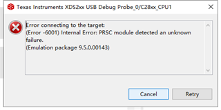
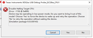

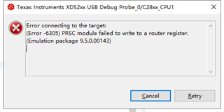
下面两个是详细的烧录异常日志记录:
C28xx_CPU1: GEL Output:
Memory Map Initialization Complete
C28xx_CPU1: GEL Output:
... DCSM Initialization Start ...
C28xx_CPU1: GEL Output:
... DCSM Initialization Done ...
C28xx_CPU1: GEL Output:
 CPU2 is out of reset and configured to wait boot.
 (If you connected previously, may have to resume CPU2 to reach wait boot loop.)
C28xx_CPU1: GEL Output:
 CM is out of reset and configured to wait boot.
 (If you connected previously, may have to resume CM to reach wait boot loop.)
C28xx_CPU1: If erase/program (E/P) operation is being done on one core, the other core should not execute from shared-RAM (SR) as they are used for the E/P code. User code execution from SR could commence after both flash banks are programmed.
C28xx_CPU1: Only CPU1 on-chip Flash Plugin can configure clock for CPU1, CPU2 and CM Flash operations. Plugin automatically configures PLL when CPU1 Flash operations are invoked. However, if users want to do only CPU2 or CM Flash operations without doing a prior CPU1 operation in the current session, they should click on 'Configure Clock' button in CPU1's on-chip Flash Plugin before invoking CPU2 and CM Flash operations. When this button is used, Flash Plugin will configure the clock for CPU1/CPU2 at 190MHz and CM at 95MHz using INTOSC2 as the clock source. Plugin will leave PLL config like this and user application should configure the PLL as required by application.
C28xx_CPU1: GEL Output:
... DCSM Initialization Start ...
C28xx_CPU1: GEL Output:
... DCSM Initialization Done ...
C28xx_CPU1: GEL Output:
 CPU2 is out of reset and configured to wait boot.
 (If you connected previously, may have to resume CPU2 to reach wait boot loop.)
C28xx_CPU1: GEL Output:
 CM is out of reset and configured to wait boot.
 (If you connected previously, may have to resume CM to reach wait boot loop.)
C28xx_CPU1: Failed CPU Reset: (Error -1044 @ 0x0) The debug probe reported an error. Confirm debug probe configuration and connections, reset the debug probe, and retry the operation. (Emulation package 9.5.0.00143)
C28xx_CPU1: Error: (Error -1135 @ 0x3FD2AE) The debug probe reported an error. Confirm debug probe configuration and connections, reset the debug probe, and retry the operation. (Emulation package 9.5.0.00143)
C28xx_CPU1: Unable to determine target status after 20 attempts
C28xx_CPU1: Failed to remove the debug state from the target before disconnecting.  There may still be breakpoint op-codes embedded in program memory.  It is recommended that you reset the emulator before you connect and reload your program before you continue debugging
C28xx_CPU1: GEL: Error while executing OnReset(-1): Could not write 0x0005FB00@Data: target is not connected
	 at *((int*) 0x5FB00)=0 [f28388d_cpu1.gel:27]
	 at OnReset(-(1))
C28xx_CPU1: Error occurred during flash operation: CPU Reset error. Error code -1
C28xx_CPU1: Error occurred during flash operation: Could not write 0x0005FB00@Data: target is not connected
C28xx_CPU1: Error occurred during flash operation: Could not write 0x00007029@Data: target is not connected
C28xx_CPU1: Error occurred during flash operation: Could not read 0x00070223@Data: target is not connected
C28xx_CPU1: Error occurred during flash operation: Could not read register ST1: target is not connected
C28xx_CPU1: Error occurred during flash operation: Could not write register ST1: target is not connected
C28xx_CPU1: Error occurred during flash operation: Could not write register ST1: target is not connected
C28xx_CPU1: Error occurred during flash operation: Could not write 0x00007029@Data: target is not connected
C28xx_CPU1: Error occurred during flash operation: Could not write 0x0005D22E@Data: target is not connected
C28xx_CPU1: Error occurred during flash operation: Could not write 0x00007062@Data: target is not connected
C28xx_CPU1: Error occurred during flash operation: Could not write 0x0005FB00@Data: target is not connected
C28xx_CPU1: Error occurred during flash operation: Could not write 0x0005F800@Data: target is not connected
C28xx_CPU1: Error occurred during flash operation: Could not write 0x0005F824@Data: target is not connected
C28xx_CPU1: Error occurred during flash operation: Could not write 0x0005F820@Data: target is not connected
C28xx_CPU1: Error occurred during flash operation: Could not write 0x0005F980@Data: target is not connected
C28xx_CPU1: Error occurred during flash operation: Could not read 0x00070223@Data: target is not connected
C28xx_CPU1: Error occurred during flash operation: Could not read 0x00070223@Data: target is not connected
C28xx_CPU1: Error occurred during flash operation: Could not write 0x0005F800@Data: target is not connected
C28xx_CPU1: Error occurred during flash operation: Could not read 0x00000000@Data: target is not connected
C28xx_CPU1: Error occurred during flash operation: Cannot enable while the target is disconnected
C28xx_CPU1: Error occurred during flash operation: Could not read 0x0005F444@Data: target is not connected
C28xx_CPU1: Error occurred during flash operation: Could not read 0x00070223@Data: target is not connected
C28xx_CPU1: Error occurred during flash operation: Could not write 0x0005F444@Data: target is not connected
C28xx_CPU1: Error occurred during flash operation: Could not read 0x0005F444@Data: target is not connected
C28xx_CPU1: Error setting the GSxMSEL register for Flash operations
C28xx_CPU1: Error occurred during flash operation: Failed to run target while trying to execute pwrite_en.alg
C28xx_CPU1: Error occurred during flash operation: Could not read 0x00070223@Data: target is not connected
C28xx_CPU1: Error occurred during flash operation: Could not write 0x0005F444@Data: target is not connected
C28xx_CPU1: Error occurred during flash operation: Could not read 0x0005F444@Data: target is not connected
C28xx_CPU1: Error occurred during flash operation: Could not read 0x00000000@Data: target is not connected
C28xx_CPU1: Flash Programmer: Error during initialization (missing algorihtm). Operation Cancelled.
C28xx_CPU1: File Loader: Memory write failed: Unknown error
C28xx_CPU1: GEL: File: F:\workspace_v10\led_ex1_blinky\CPU1_FLASH\led_ex1_blinky.out: Load failed.
C28xx_CPU1: Error occurred during flash operation: Could not read register PC: target is not connected
C28xx_CPU1: Error occurred during flash operation: Could not read 0x00000000@Data: target is not connected
C28xx_CPU1: Error occurred during flash operation: Cannot enable while the target is disconnected
C28xx_CPU1: Error occurred during flash operation: Could not read 0x0005F444@Data: target is not connected
C28xx_CPU1: Error occurred during flash operation: Could not read 0x00070223@Data: target is not connected
C28xx_CPU1: Error occurred during flash operation: Could not write 0x0005F444@Data: target is not connected
C28xx_CPU1: Error occurred during flash operation: Could not read 0x0005F444@Data: target is not connected
C28xx_CPU1: Error setting the GSxMSEL register for Flash operations
C28xx_CPU1: Error occurred during flash operation: Failed to run target while trying to execute pwrite_en.alg
C28xx_CPU1: Error occurred during flash operation: Could not read 0x00070223@Data: target is not connected
C28xx_CPU1: Error occurred during flash operation: Could not write 0x0005F444@Data: target is not connected
C28xx_CPU1: Error occurred during flash operation: Could not read 0x0005F444@Data: target is not connected
C28xx_CPU1: Error occurred during flash operation: Could not write 0x0005F800@Data: target is not connected
C28xx_CPU1: Error occurred during flash operation: Could not write register PC: target is not connected
C28xx_CPU1: Error occurred during flash operation: Could not read 0x00000000@Data: target is not connected
C28xx_CPU1: Error occurred during flash operation: Cannot enable while the target is disconnected
C28xx_CPU1: Error occurred during flash operation: Could not read 0x0005F444@Data: target is not connected
C28xx_CPU1: Error occurred during flash operation: Could not read 0x00070223@Data: target is not connected
C28xx_CPU1: Error occurred during flash operation: Could not write 0x0005F444@Data: target is not connected
C28xx_CPU1: Error occurred during flash operation: Could not read 0x0005F444@Data: target is not connected
C28xx_CPU1: Error setting the GSxMSEL register for Flash operations
C28xx_CPU1: Error occurred during flash operation: Failed to run target while trying to execute pwrite_dis.alg
C28xx_CPU1: Flash operation timed out waiting for the algorithm to complete. Operation cancelled.
C28xx_CPU1: Perform a debugger reset and execute the Boot-ROM code (click on the RESUME button in CCS debug window) before erasing/loading the Flash.  If that does not help to perform a successful Flash erase/load, check the Reset cause (RESC) register, NMI shadow flag (NMISHDFLG) register and the Boot-ROM status register for further debug.
C28xx_CPU1: Error occurred during flash operation: Could not read 0x00070223@Data: target is not connected
C28xx_CPU1: Error occurred during flash operation: Could not write 0x0005F444@Data: target is not connected
C28xx_CPU1: Error occurred during flash operation: Could not read 0x0005F444@Data: target is not connected
C28xx_CPU1: GEL Output:
Memory Map Initialization Complete
C28xx_CPU1: Failed CPU Reset: (Error -6311) PRSC module failed to write to a register. (Emulation package 9.5.0.00143)
C28xx_CPU1: Error: (Error -1044 @ 0x0) The debug probe reported an error. Confirm debug probe configuration and connections, reset the debug probe, and retry the operation. (Emulation package 9.5.0.00143)
C28xx_CPU1: Error: (Error -1135 @ 0xD057) The debug probe reported an error. Confirm debug probe configuration and connections, reset the debug probe, and retry the operation. (Emulation package 9.5.0.00143)
C28xx_CPU1: Unable to determine target status after 20 attempts
C28xx_CPU1: Failed to remove the debug state from the target before disconnecting.  There may still be breakpoint op-codes embedded in program memory.  It is recommended that you reset the emulator before you connect and reload your program before you continue debugging
C28xx_CPU1: GEL: Error while executing OnReset(-1): Could not write 0x0005FB00@Data: target is not connected
	 at *((int*) 0x5FB00)=0 [f28388d_cpu1.gel:27]
	 at OnReset(-(1))
C28xx_CPU1: GEL: Error while executing OnTargetConnect(): Reset failed: retcode=-1
	 at GEL_Reset() [f28388d_cpu1.gel:117]
	 at OnTargetConnect()
出现问题后,对板子进行原理图、PCB的检查,以及电源模块、JTAG模块的电阻电容电感的测量,以及用示波器对25M晶振的工作稳定性测量。
都没问题,boot mode也拨到了GPIO84和GPIO72都拉高的情况(断电后,程序从flash启动)。
总体来看,电路板只在下载程序(用JTAG口,仿真器xds200)的时候,容易经常出现错误。有时候,偶然情况下,程序能下载进去,断电再上电,程序就可以正常运行,电路板从工作的状态来看,也一切正常。
主芯片与JTAG的原理图连接图、晶振图、电源模块:
特来请教,是否还有别的地方可能出错。望得到一些指导。
感谢!