

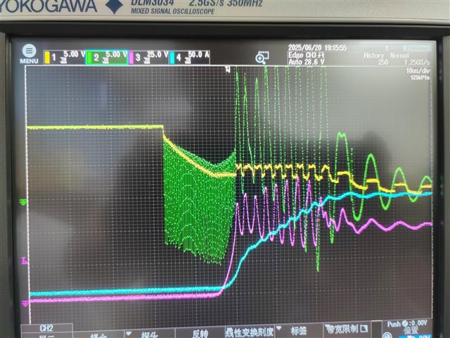
如上两张图片,黄色:放电MOS关Vgs,绿色:DSG引脚,红色:放电MOS管Vds,蓝色:PACK输出电流;
现象:两个版本的测试图片,左图是新版本,DSG引脚震荡,右图是旧版本,无次震荡;
问题:经过查找、对比原理图、PCB文件,没有找出差异,现在不清楚为什么DSG会震荡?需要协助查找原因以及解决办法
已经处理过的:通过对换MOS,已经明确确定是新版本的PCB或者原理图哪里有影响,旧版本的PCB没有问题, 并且PIN46-PIN47脚的电容电压是稳定的,没有发现震荡现象
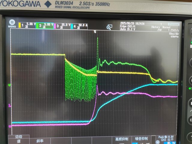
如上两张图片,黄色:放电MOS关Vgs,绿色:DSG引脚,红色:放电MOS管Vds,蓝色:PACK输出电流;
现象:两个版本的测试图片,左图是新版本,DSG引脚震荡,右图是旧版本,无次震荡;
问题:经过查找、对比原理图、PCB文件,没有找出差异,现在不清楚为什么DSG会震荡?需要协助查找原因以及解决办法
已经处理过的:通过对换MOS,已经明确确定是新版本的PCB或者原理图哪里有影响,旧版本的PCB没有问题, 并且PIN46-PIN47脚的电容电压是稳定的,没有发现震荡现象
