

Part Number: TIDM-02013
Hi,as shown in the figure,lab 1 to 4 are all aimed at verifying the PFC mode.
However, why did lab 1 and 2 use DC as the input, rather than AC voltage?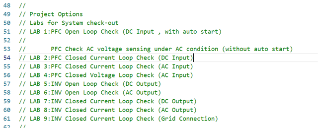
Original question:

Part Number: TIDM-02013
Hi,as shown in the figure,lab 1 to 4 are all aimed at verifying the PFC mode.
However, why did lab 1 and 2 use DC as the input, rather than AC voltage?

