LMG1210:HO/LO gate outputs not as expected

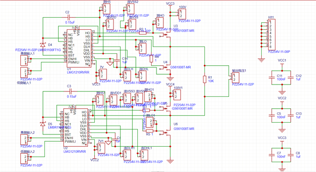
Part Number: LMG1210


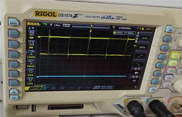
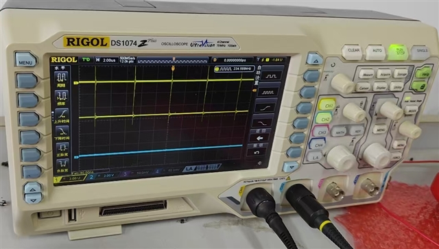
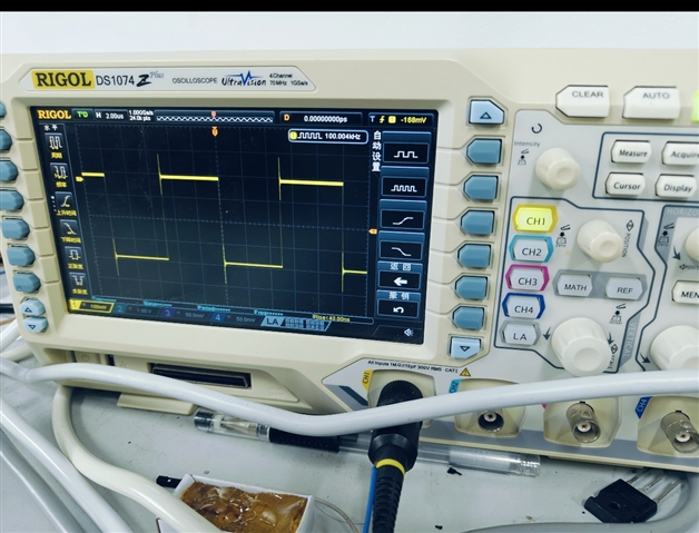
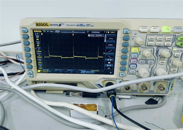
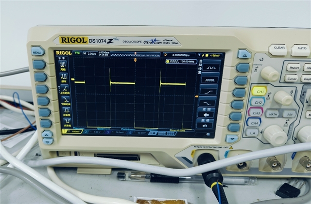
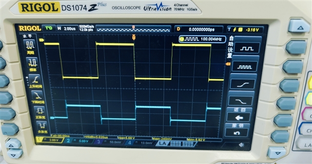
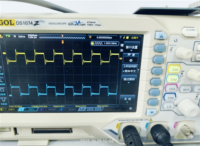
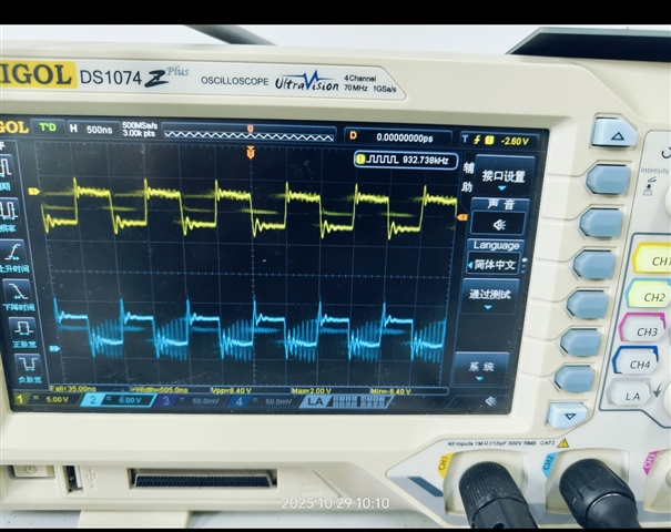
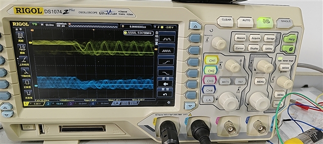
I’m using the LMG1210 in Independent Input Mode (IIM) and driving HI and LI with two complementary 100-kHz PWM signals, but on the oscilloscope the HO and LO outputs are not clean PWM and the apparent frequency is doubled; I later noticed that on my PCB the two exposed (bottom) pads were mistakenly left unconnected to HS and VSS, so I’d like to confirm whether this missing connection alone could cause the abnormal HO/LO behavior and frequency doubling, how critical those exposed-pad connections are electrically (not just thermally), and what additional checks or measurements you would recommend—schematic and scope captures can be provided if helpful; thanks in advance.  

  • Hello!

    We have received your case and will take some time. Thank you for your patience.

  • First, could you please provide your schematic? Second, did you still see this behavior when you correctly connected the thermal pads? Leaving those pads unconnected could be the cause of the HO/LO behavior because GaN drivers are switching so quickly that sufficient thermal dissipation is important for achieving desired outputs. Without the proper thermal dissipation paths, you can see increased inductance, voltage ringing and power loss.

    As for the frequency doubling, it's not likely that the unconnected thermal pads directly cause this, but the OTP may be triggering and causing rapid uncontrolled switching that may cause the frequency to appear doubled. Can you provide labelled waveforms of LI, HI, VDD, LO, HO, and HB-HS so I can investigate this further?

  • I apologize for the delayed response to your reply. I have now properly connected the bottom pad, and the issue of the output frequency doubling has been resolved.
    I have tested two operating modes of this chip: IIM mode and PWM mode. In IIM mode, my input consists of two complementary 100kHz square waves. In PWM mode, my inputs are an enable signal and a 100kHz square wave.
    The waveforms measured at the HO and LO output ports are shown in the attached figures. The waveform at the low-side (LO) meets expectations, but the high-side HO port and HS port show identical waveforms. While the output frequency is correct, the amplitude is not as expected.
    Could you please help explain why there might be an issue with the output waveform amplitudes of the HO and HS ports? I have attached my circuit schematic and the input/output waveform diagrams below for reference.The first diagram is my circuit schematic, the second one shows the input square waves, the third displays the output waveforms of the HS and HO ports, and the fourth presents the output waveform of the LO port. Thank you for your reply.
  • Glad to hear that the thermal pads connection has helped solve the output frequency doubling issue.

    Regarding your HO-HS waveform not showing expected values listed below are my asks regarding this

    1. Can you please let me know what values you would like the HO-HS waveform to have?

    2. Can you please provide the HB-HS waveform. this will show us if the bootstrap circuit is providing the sufficient supply for HS driver.

    3.  Can you check if there is enough LO on-time to keep the capacitor charged? If the lower MOS is not on for a long enough time, the bootstrap capacitor will not be able to fully charge. The LMG1210 also has a switch that only turns on and allows the capacitor to charge when the LO output is on.
  • Thank you for your reply. First, I made an error in the test this morning, so I re-conducted the test. I found that there is no waveform between HO and HS. The HO-HS waveform I expected is a square wave with the same frequency as the input waveform and a voltage within the range specified in the datasheet.
    Second, I also saw no waveform across HB and HS (i.e., across the capacitor). Besides, the forward voltage drop of the transistor does not match the estimation in the chip datasheet. Therefore, I currently believe the issue lies in the bootstrap circuit. However, the selection and specifications of both the capacitor and the transistor meet the requirements in the chip datasheet, so I now suspect the problem is caused by the load.
    Finally, if there is consistently no waveform across the capacitor (i.e., across HB and HS), does this mean there is no charging at all, rather than insufficient charging? I haven’t soldered the GaN device onto the circuit board yet. Initially, I planned to test the chip’s output waveform first before soldering the GaN device. But after carefully checking the circuit diagram in the datasheet, I realized that not connecting the load might cause problems with the bootstrap circuit. So now I intend to solder the GaN device onto the circuit board first, then conduct the test to check the output result. Do you think the current issue—where the bootstrap circuit is not working properly—is related to the unmounted load (i.e., the unsoldered GaN device)?
    I apologize for making many basic mistakes due to my carelessness as a beginner. Thank you for your reply.
  • Good evening. When I tested this afternoon, I switched the chip to the Independent Input Mode (IIM). The test results met my expectations. In Figure 1, the yellow waveform is the waveform of LO, and the blue waveform is the waveform of HO-HS. The second figure shows the voltage across the bootstrap capacitor measured by a multimeter, which also meets the requirements. Currently, the chip works normally in IIM mode, but there are still issues in PWM mode. Thank you for your previous reply. I will gradually troubleshoot the causes of the problems in PWM mode later. If I encounter any issues, I would like to continue consulting you. Thank you very much.

  • Hello, I have integrated the GaN device into my circuit, but I am observing behavior I do not yet understand. When only the first driver IC is powered, the HO–HS and LO outputs are normal, as shown in Figure 1. However, when only the second driver IC is powered, the HO–HS and LO outputs become distorted, as shown in Figure 2. Furthermore, when both driver ICs are powered simultaneously, no signals are observed at HO–HS or LO on either device. I am unable to determine the cause. Could you please suggest several troubleshooting approaches?Would you like me to provide the power supply’s voltage and current levels used at that time?

  • Hello ,

    Please post a new ticket due to time