UCC28740: UCC28740:PMP41009

Part Number: UCC28740
Other Parts Discussed in Thread: PMP41009

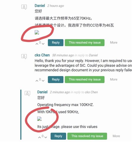
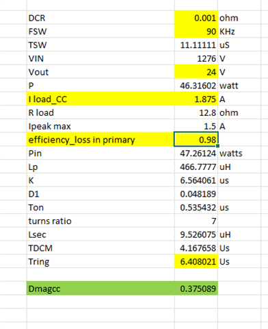
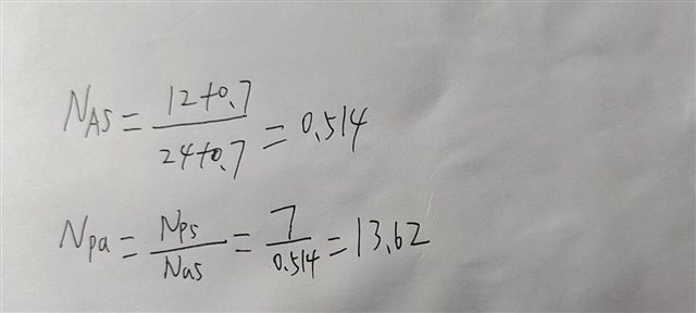
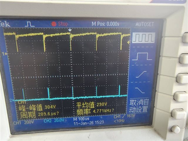
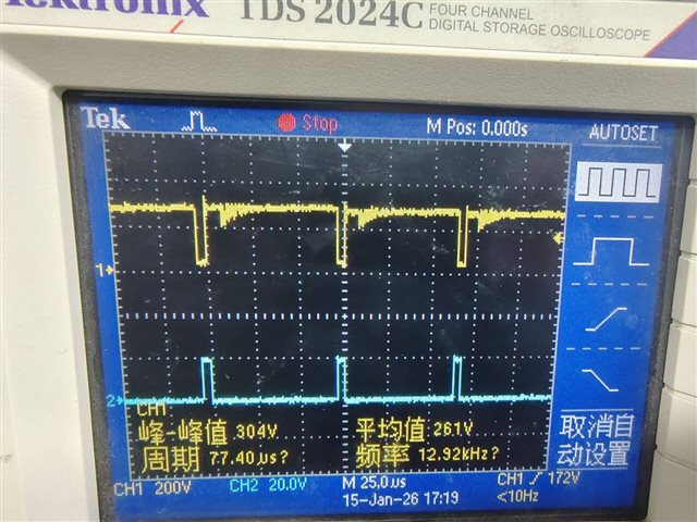
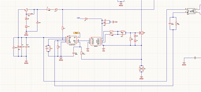
Hello, I plan to use the UCC28740 chip to design a wide-range dual-transistor flyback converter with a structure similar to that of the PMP41009. Its specifications are as follows: output power of 40W, input voltage of 85-900V AC, output voltage of 24V, and maximum switching frequency of 100kHz. However, during the transformer design process, when calculating the primary inductance (Lp) in accordance with the UCC28740 datasheet, the resulting Lp value is 330μH. At this point, the minimum on-time (ton(min)) does not meet the minimum target of 280ns (maximum tCSLEB). Additionally, the calculated minimum required Lp value is 792.97μH. Does this mean that my design specifications are not achievable?Why is this the case, and which part of the designed specifications is unreasonable?

补充说明:

image.png

  • Hello, we have received your case and the investigation will take some time. Thank you for your patience.

  • 您好

    请选择最大工作频率为65至70KHz。

    试着遵循这个设计。我选择了你的CC功率为46瓦

  • Hello, thank you for your reply. However, I am required to use SiC MOSFETs in the design, so I hope the maximum frequency can reach 100 kHz to leverage the advantages of SiC. Could you please advise on the methods to achieve a maximum operating frequency of 100 kHz? In addition, the recommended design document in your previous reply failed to open; would you mind resending it? Thank you and best regards.

  • 您好

    Operating frequency max 100KHZ.

    With !0KHz I used 90KHz,

    Its just image. please use this values

  • Hello, why can't these two pictures you sent be displayed?

  • Hello, based on the parameters you provided, I calculated that the turns ratio between the primary winding and the auxiliary winding is 13. Is this parameter reasonable?

  • Hello, I have redesigned the transformer using the parameters you provided, but there has been no improvement at all — the duty cycle is still extremely small. In your opinion, what other aspects could be the cause of this problem?

  • 您好

    你能调节电压吗?你面临的实际问题是什么?

  • Hello, my problem is that the duty cycle of my MOSFET is incorrect. My design requires it to work properly within the 85-900VAC input range, but the current duty cycle is too small. Adjusting the voltage feedback section has no effect; only changing the current sampling resistor of the CS pin on the control chip and the relevant parameter values of the RC circuit can alter the duty cycle. However, after making these changes, the output voltage is too high under no-load conditions, and the duty cycle does not increase significantly either. So is there any solution to this problem? I am using a SiC MOSFET—does this have any impact?The first image shows the Vgs and Vds waveforms of the MOSFET with 220VAC input under no-load condition, and the second image displays the Vgs and Vds waveforms of the MOSFET with 220VAC input under half-load condition. The upper trace is Vds and the lower trace is Vgs.

  • My design is almost the same as that of PMP41009, with the only major difference being the addition of a driver chip in the driving circuit to drive the SiC MOSFETs. Could this be the cause of the problem? However, the waveform output by the control chip DRV is exactly the same as and perfectly matches the Vgs waveform of the MOSFETs. So I really have no idea where the problem lies right now. Could you help me figure it out? Thank you.