Part Number: BQ79616
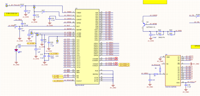
使用BQ79616设计储能系统的BMS,AFE接上16s电池模组(DC52V)后,在没有唤醒的情况下CVDD和LDOIN电压只有2.8-2.9V左右,小于数据手册中要求的关机状态下,最低电压3.4V。这是为什么?BAT电压52V应该没问题,那只有RNPN电阻和BJT三极管了,难道是选型有问题?
Part Number: BQ79616
使用BQ79616设计储能系统的BMS,AFE接上16s电池模组(DC52V)后,在没有唤醒的情况下CVDD和LDOIN电压只有2.8-2.9V左右,小于数据手册中要求的关机状态下,最低电压3.4V。这是为什么?BAT电压52V应该没问题,那只有RNPN电阻和BJT三极管了,难道是选型有问题?