Part Number: LM3409HVEVAL
Other Parts Discussed in Thread: LM3409
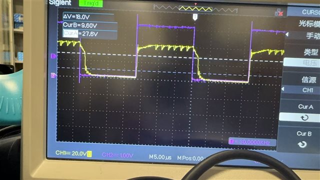
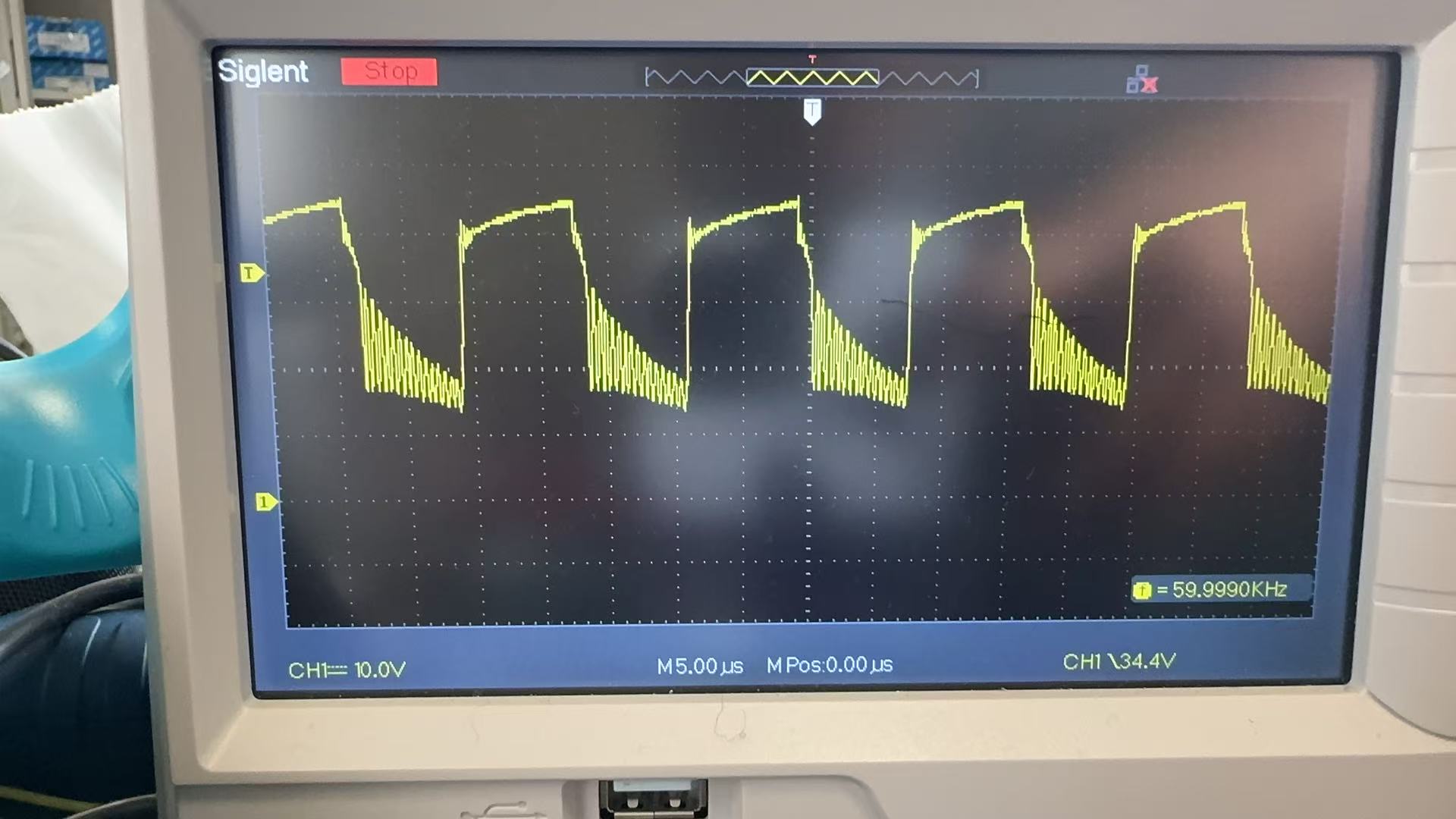
Keep the original parameters of the LM3409HVEVAL unchanged, switch J1 to Mode 2, use an external 60 kHz PWM signal for triggering, connect a load of 14 LEDs, and supply voltage via a signal generator. The following issues occurred:
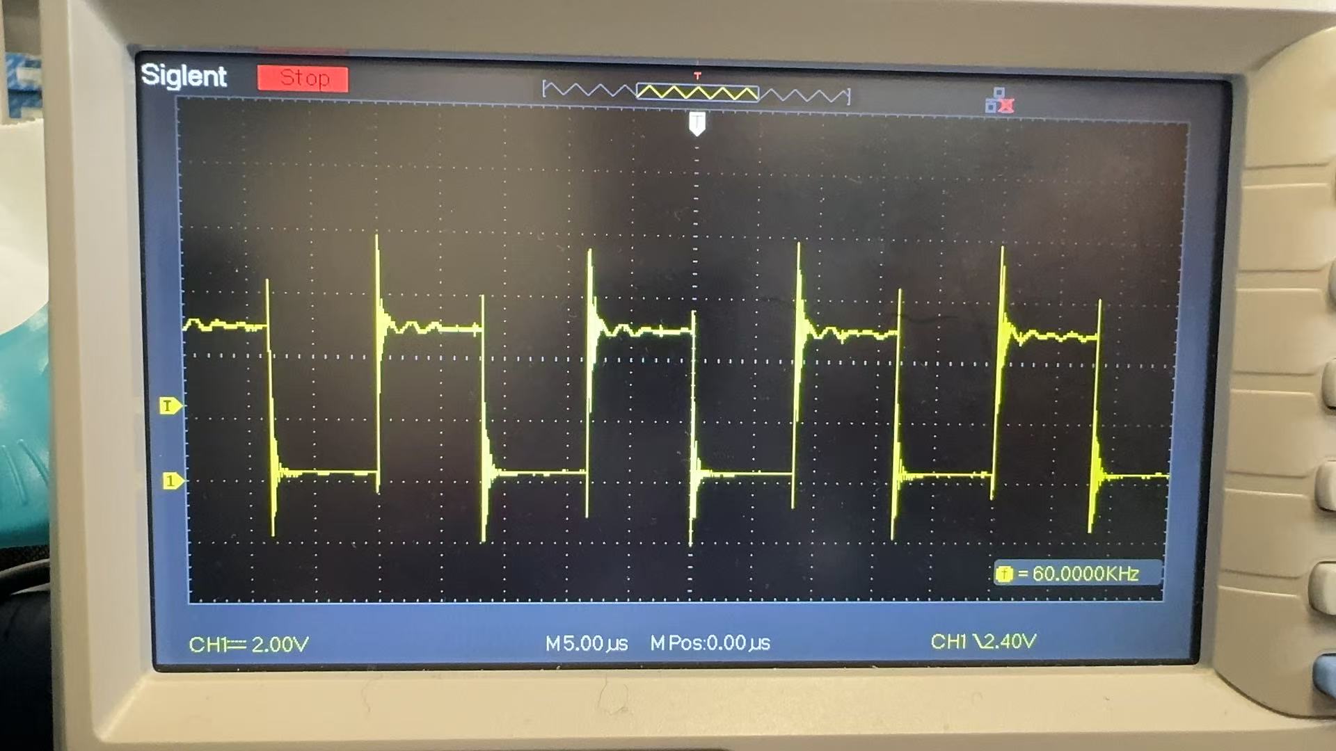
- A huge surge voltage of up to 90 V appeared at the LED+ output, and a large surge also occurred in the PWM input signal.
- yellow PWMin
- yellow LED+
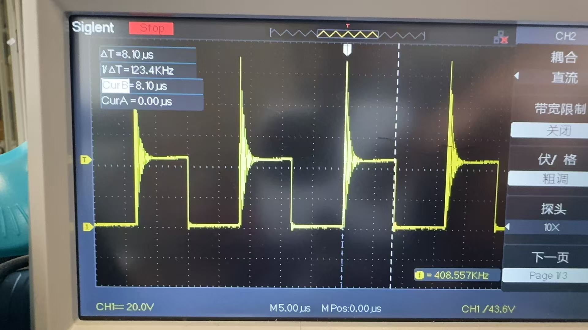
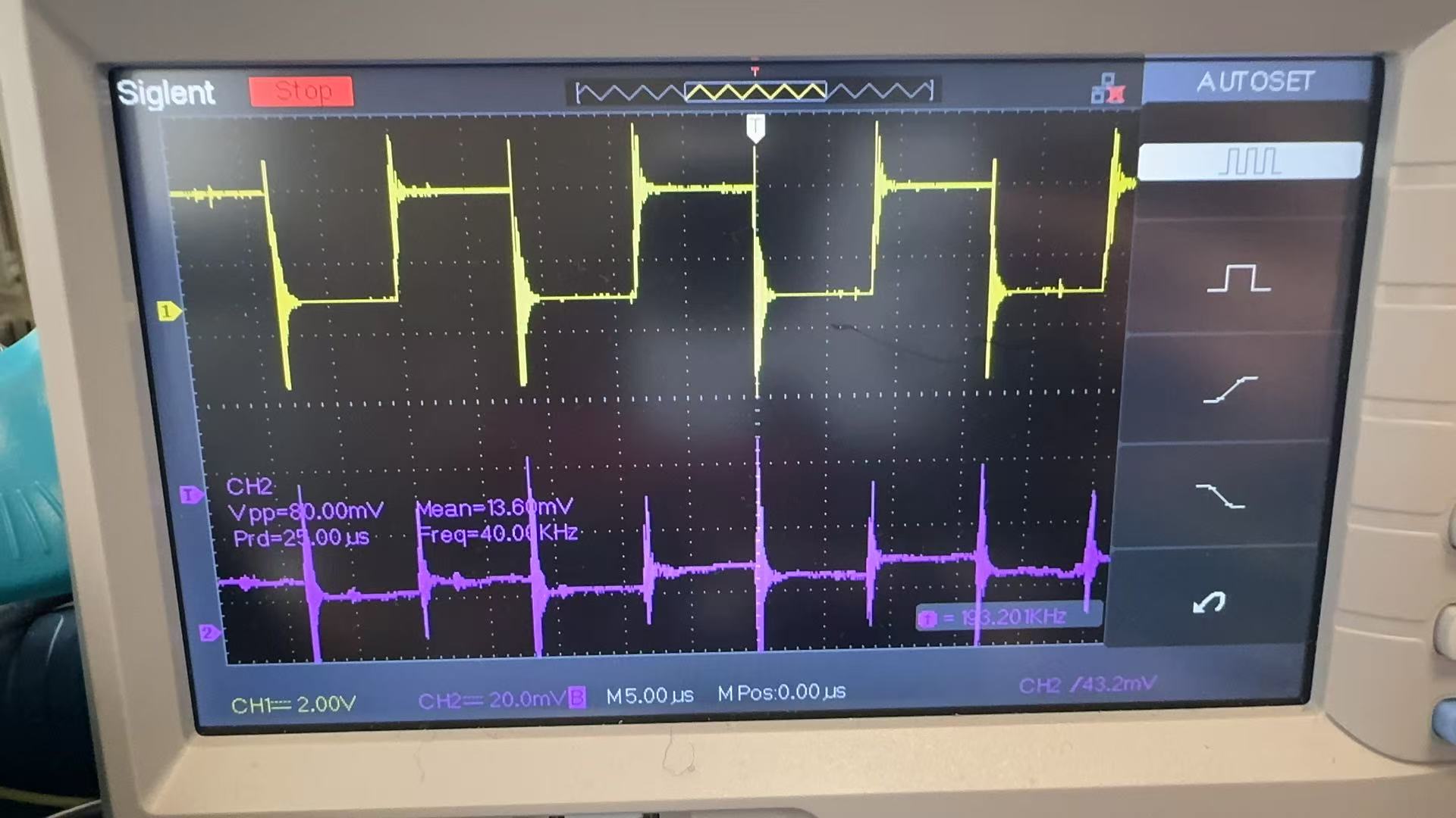
- Q3-G
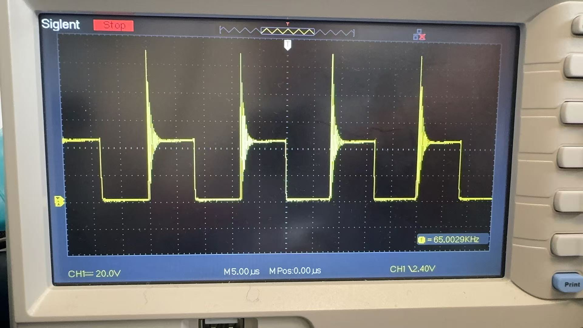
- The test waveforms are as follows: After changing R1 to 20 Ω and adding a 10 kΩ pull-down resistor from the G-pin of Q3 to GND, the surge at the G-pin of Q3 gradually became smooth, but the waveform at the LED+ output of the load remained unchanged.
- Q3-G
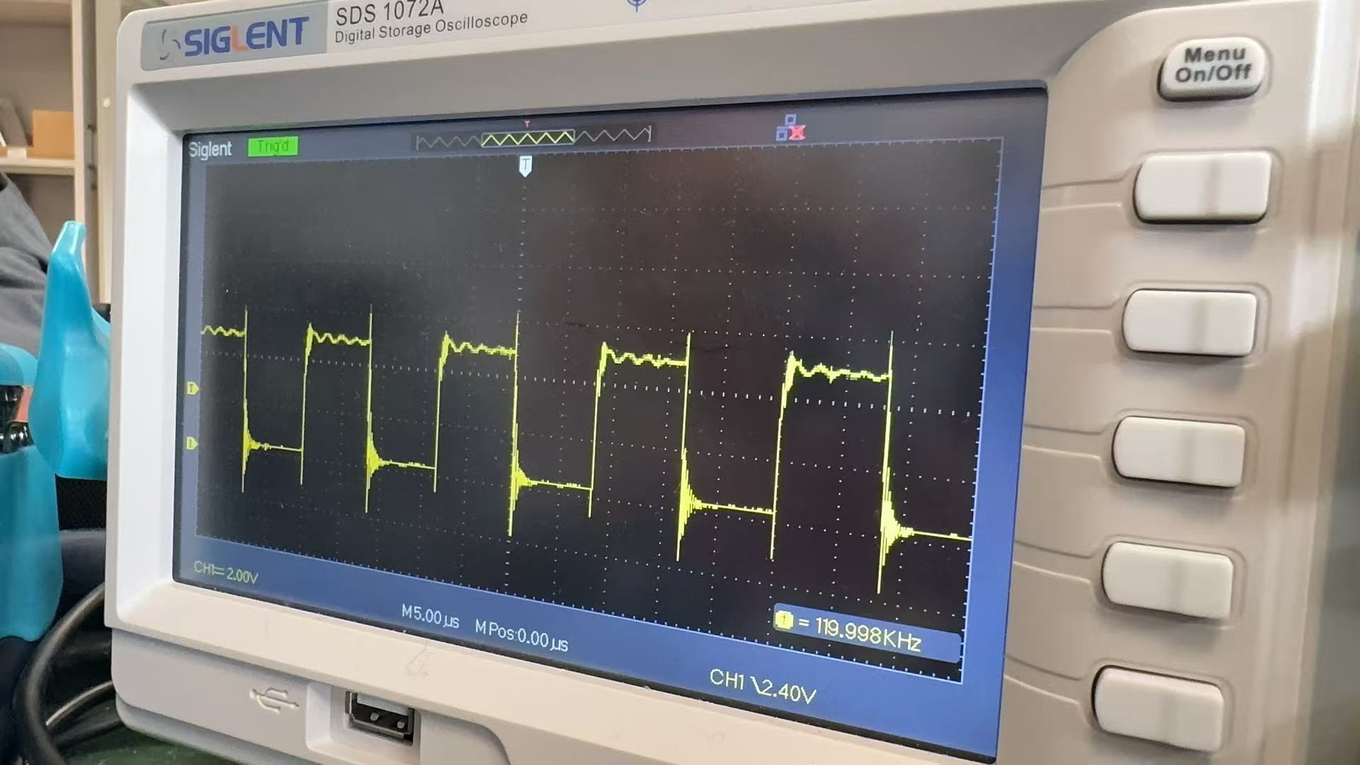
- LED+
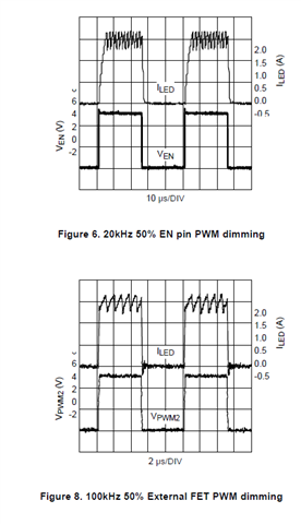
- When using a pulse signal directly input to the EN pin for dimming, although the performance at 60 kHz was poor (the LEDs could not be completely turned off), no large surge occurred.
- EN wave
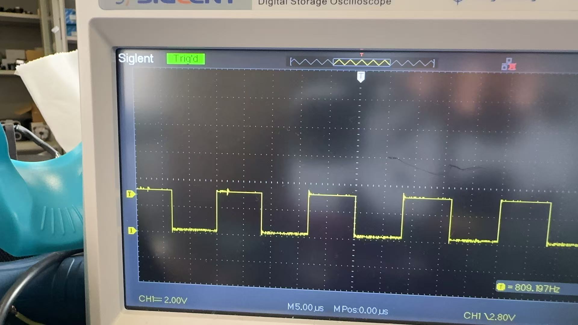
- LED+
- To solve this problem, I replaced C8 with a 22 μF capacitor. Upon power-on, the device had no output, the chip was damaged, and an inductor squeal was heard.
My Request: How to solve the large surge problem under external PWM driving, and what debugging methods should be adopted?