This thread has been locked.
If you have a related question, please click the "Ask a related question" button in the top right corner. The newly created question will be automatically linked to this question.
我用UC2844做软启动,但是启动时间特别慢。不知道有没有芯片软启动计算时间的公式啊?
你好
针对UC2844这款芯片 是外部设置软启动的
RC近似为启动时间 所以 你可以 减小R 或者C 尝试减小启动时间
希望能解决你的问题
hi
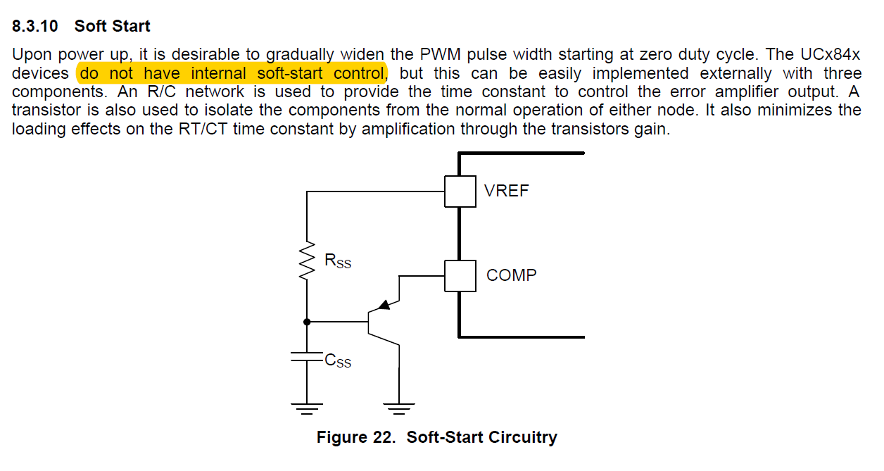
我们芯片UC2844内部没有软启动设置,但是通过外部配置Rss和Css的值可以设置软启动的时间。你可以理解成启动的时候VREF电压通过RC电路给电容充电,使PNP管基极电压不断上升直至PNP关断,COMP不再被钳位。电路正常工作。
希望能帮助到您,谢谢。
Hi
将你的电路传上来看看,主要看软起动方面的控制。
Hi,
请参考Ji Jing的回答。这个电路的原理是,刚开始启动时,PNP管Vbe<-0.7V,PNP管导通,将COMP嵌位在0.2~0.3V;随着VREF为Css充电,PNP管的基极电压逐渐抬高,达到某一门限时PNP管关断,COMP电压不再被嵌位,芯片启动完成开始正常工作。
您好,
可通过RC充电时间常数估算软起动时间
这个软启动电路在上电瞬间将COMP脚电压钳位为三极管的Veb,此时VFB被补偿网络钳位为约5V。在整个软启动过程中,VFB通过RSS给电容CSS充电,直至COMP脚电压达到Ipeak*Asc*Rsc,Ipeak为稳态时开关管的峰值电流,Asc为电流检测增益,Rsc为电流采样电阻。此时COMP脚电压变为受峰值电流钳位,软启动完成。因此可以算得软启动时间约为Rss*Css*ln[5/(5-Ipeak*Asc*Rsc+Veb)]。