Other Parts Discussed in Thread: TPS65185
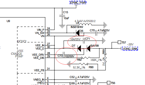
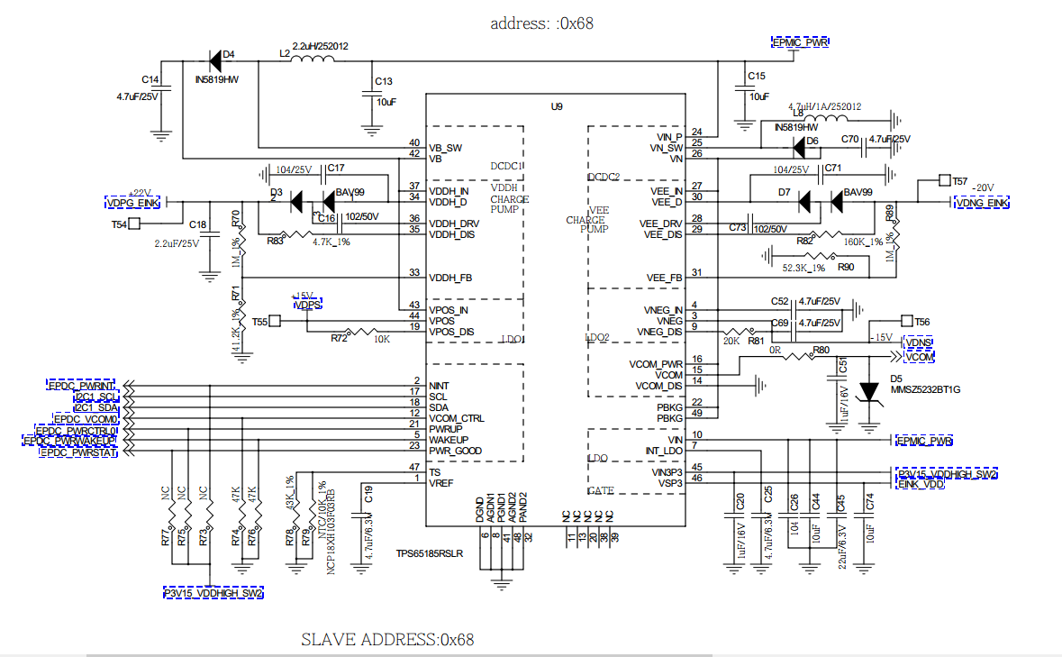
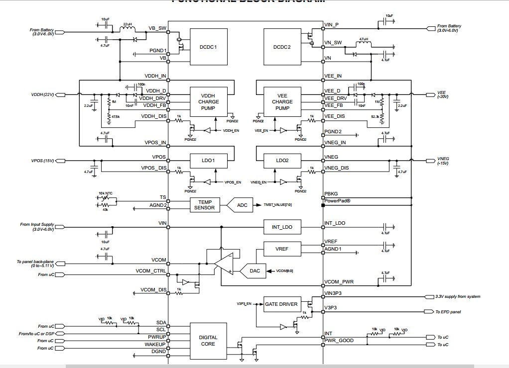
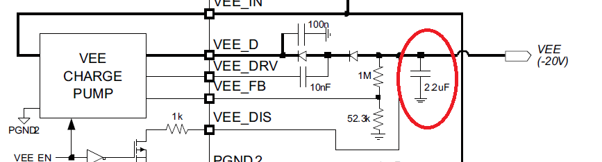
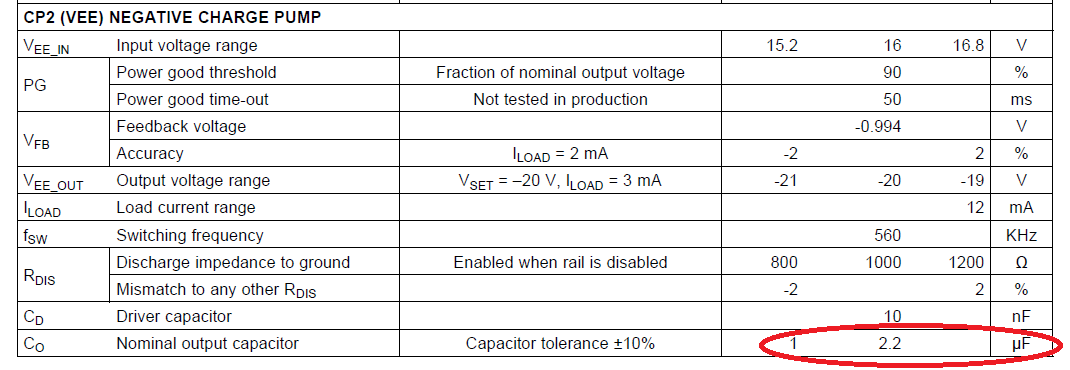
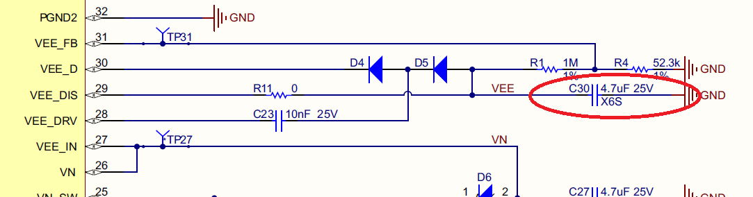
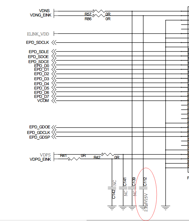
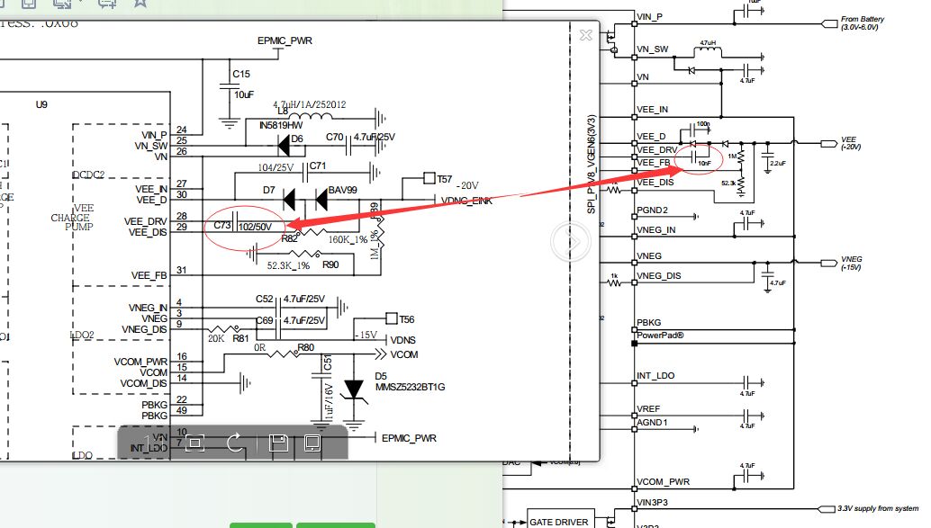
通过获取寄存器0x08h (INT2) 的值, 值为0x08, 数据手册里面标明问题是:
| 1 – under-voltage on VEE charge pump detected |
这样的话,如何修改能够使VEE输出正常呢? 能否有办法修改VEE的输出?
Other Parts Discussed in Thread: TPS65185
通过获取寄存器0x08h (INT2) 的值, 值为0x08, 数据手册里面标明问题是:
| 1 – under-voltage on VEE charge pump detected |
这样的话,如何修改能够使VEE输出正常呢? 能否有办法修改VEE的输出?