

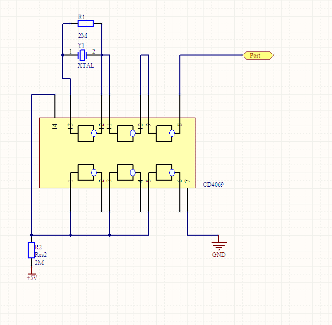
我想做一个无线充电的模块,这个图是我在网上找的,是该模块的振荡部分
我想请教以下几个问题:
1、图上那个晶振和R1再经过3个非门出来后为什么是方波,每个非门的作用是什么?
2、R1和晶振的参数是怎样确定的,我照图上用了2M的晶振,当R1是1M时出来的频率有约100KHZ,R1是620K时出来的频率快400K了?
3、CD4069的Datasheet上面说不用的输入端要接Vcc或者正极,这个图上为什么要接R2再接Vcc?
我想做一个无线充电的模块,这个图是我在网上找的,是该模块的振荡部分
我想请教以下几个问题:
1、图上那个晶振和R1再经过3个非门出来后为什么是方波,每个非门的作用是什么?
2、R1和晶振的参数是怎样确定的,我照图上用了2M的晶振,当R1是1M时出来的频率有约100KHZ,R1是620K时出来的频率快400K了?
3、CD4069的Datasheet上面说不用的输入端要接Vcc或者正极,这个图上为什么要接R2再接Vcc?
