If you have a related question, please click the "Ask a related question" button in the top right corner. The newly created question will be automatically linked to this question.
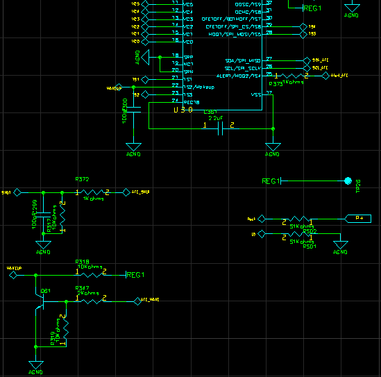
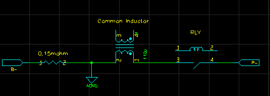
BAT-, VC0 and Vss should all be referenced to roughly the same potential reference point. So Vss should be connected to BAT-. I can see that Vss is referenced after the sense resistor, in other words to PACK-. We recommend to have VSS referenced to BAT-. We've seen issues if Vss is referenced to PACK- for some customers.
Can they measure the voltage directly from the pins to Vss, so VC1 to Vss, VC0 to Vss, VC1 to VC0 during high charging and see if it matches the measurements by the IC. They mention they see a voltage difference between 0.3-V to 1.5-V, is this related to the amount of current? Or it varies randomly?
At what currents do they see the issue?
Is there any voltage drop on the traces themselves?