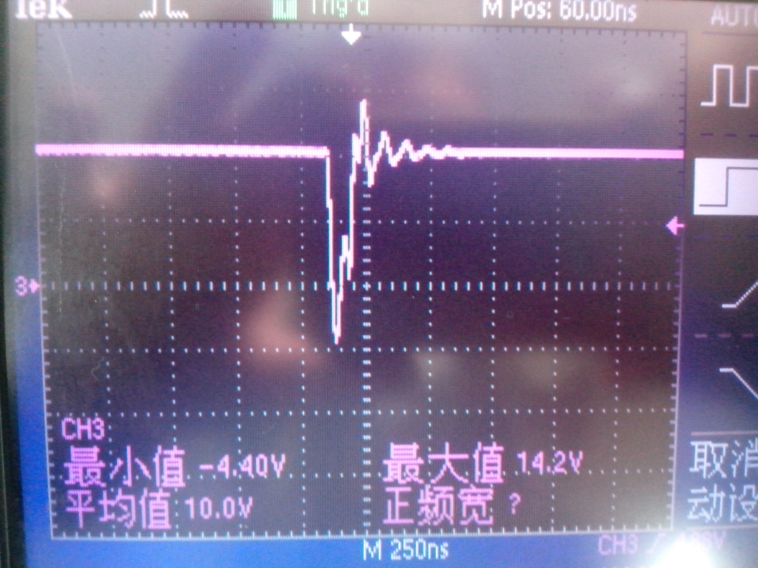
由于需要想弄个DC-DC升压,在TI的WEBENCH上模拟出使用TPS55340的电路,然后买元件搭电路
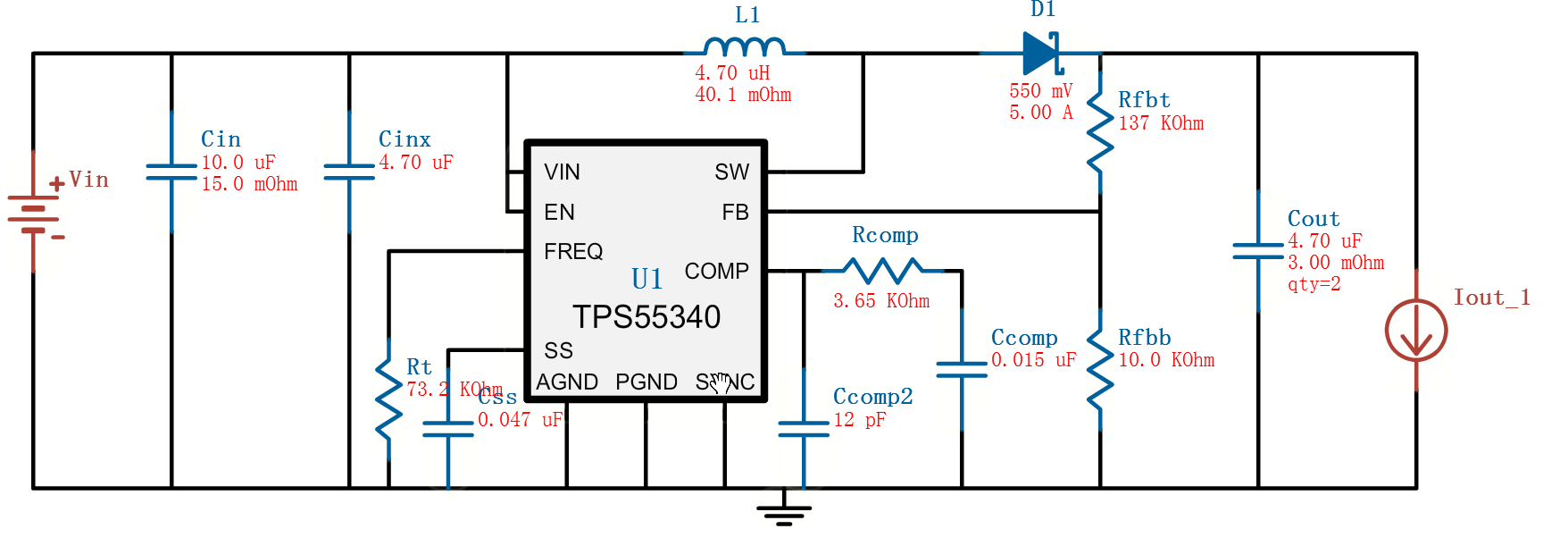
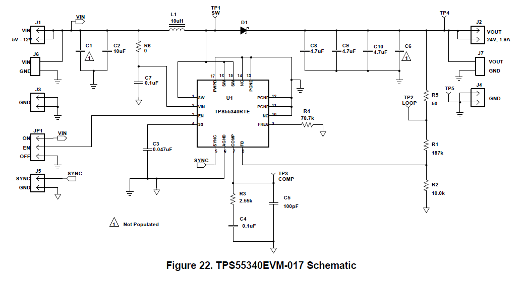
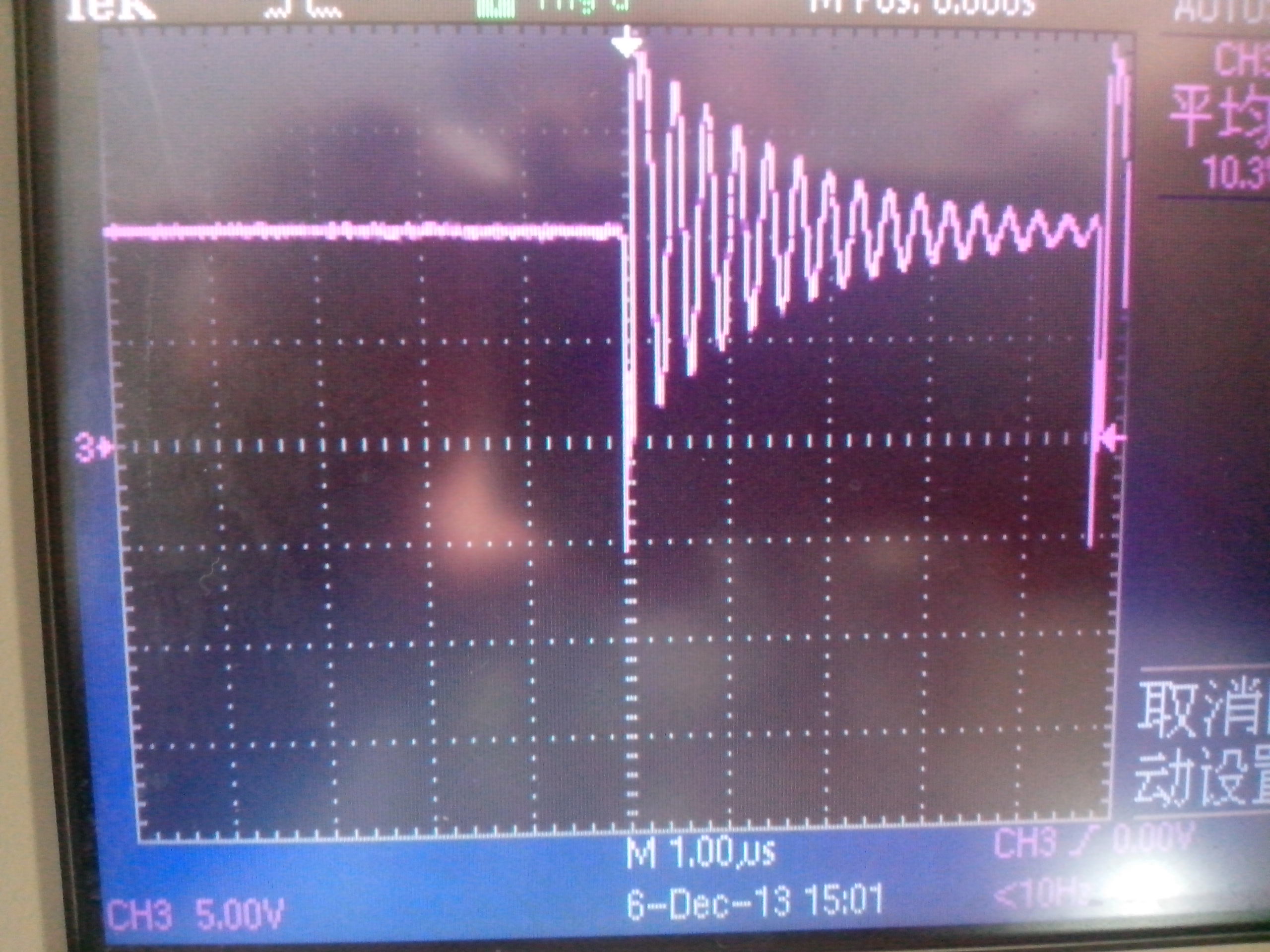
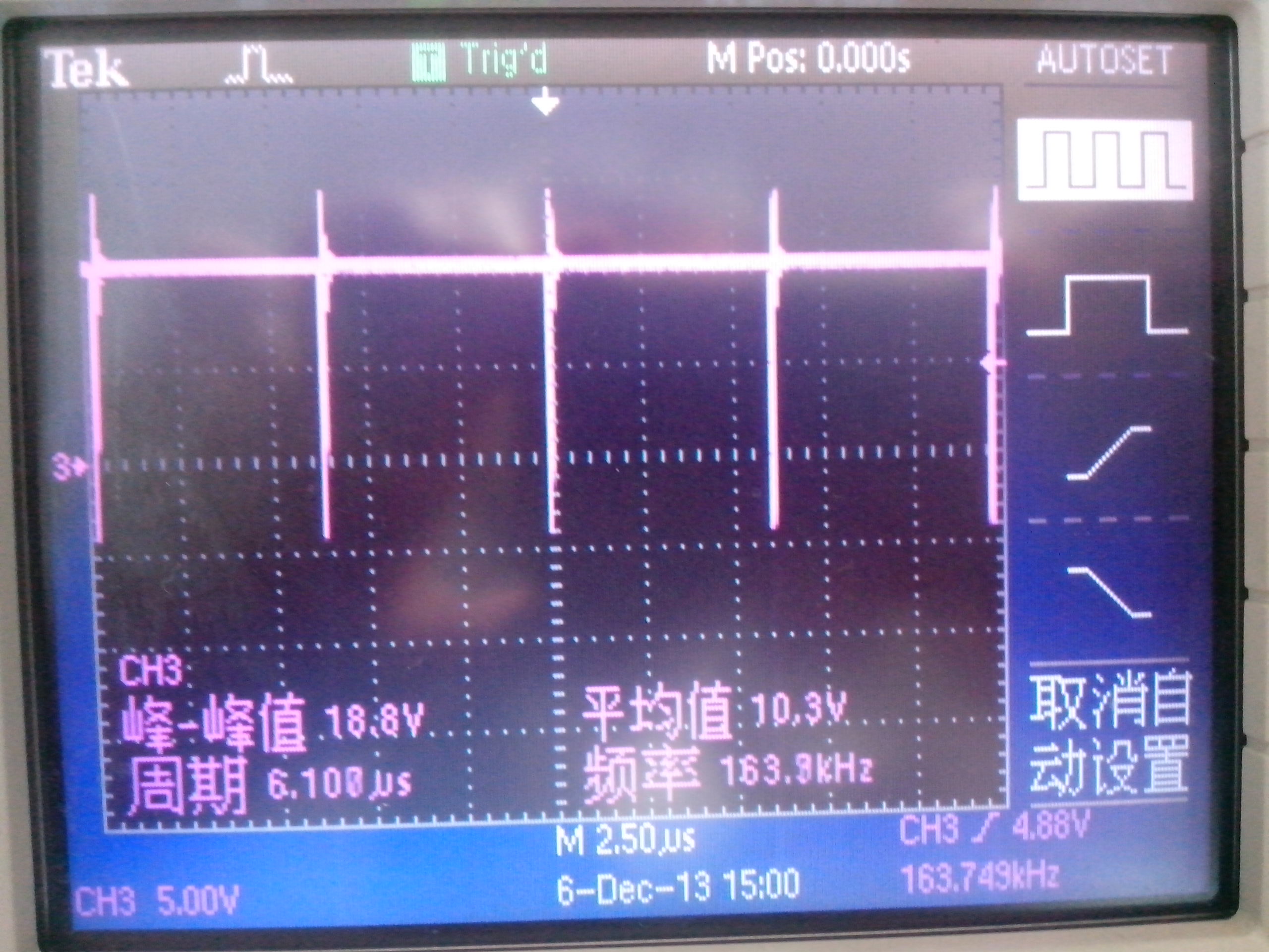
这是原始电路图,基本上我没怎么变动,肖特基二极管用的是1N5822,Ccomp2电容用的手头现成的15pF。结果测试,输出电压基本稳定在18.2V左右,但是我加了个50欧的负载,输出电压直接降到9.74V(输入电压为10V),查看数据文档,计算这时的FB口电压实际已经低于0.9V,说明加载后IC根本没工作。把负载去掉,电压马上回复正常,这时什么原因呢?
This thread has been locked.
If you have a related question, please click the "Ask a related question" button in the top right corner. The newly created question will be automatically linked to this question.
Hi
建议你在空载或者非常轻载的情况下测试以验证你的电感是否饱和了,原因是你在带负载后电压被拉低。
HI
注意一下你的layout. 特别是PowerPad要充分与GND焊接用于散热,这个可以参考TI的EVM board.
Hi
买电感的时候应该可以看到起规格,你有用TI 的wenench仿真软件,在软件里也可以看到一些参数,如电感的峰值电流。那么你买的电感的饱和电流就必须大于这个值。
买功率电感的时候没有注意这个问题,你需要查询一下,否则你需要自己测试一下电感饱和电流,测试方法在网上搜索一下.
空载测试一般不容易饱和,可以输出输出是否正常?
对啊,我把负载调整为10K左右,输出电压都还有1V下降,电流只有不到2mA啊,不可能这么小也会饱和吧
Hi
你前面已经空载测试过了,只是不能加载。
如之前提到的确认一下电感的饱和电流(这个在你买的时候就应该会看到规格的),以及芯片的PowerPad焊接等layout.
我想问下,你是否是用板子搭出来,不是自己画PCB做的吧?自己搭板子,做成现在的高频开关电源的成功可能性微乎其微
电路出现衰减震荡的话很容易理解,电感和寄生电容产生谐振了。衰减是因为mosfet导通的时候有Rds。